
2017 Microchip Technology Inc.
DS20005570C-page 1
HV7360/HV7361
Features
• High-Density Integration AC-coupled Pulser
• 0V to ±100V Output Voltage
• ±2.5A Source and Sink Minimum Pulse Current
• Up to 35 MHz Operating Frequency
• 2 ns Matched Delay Times
• 2.5V, 3.3V or 5V CMOS Logic Interface
• Built-in Two-terminal Low-noise Interface for
HV7361
• Low Power Consumption and No Floating Power
Supply Rails or Decoupling Capacitors
Applications
• Medical Ultrasound Imaging
• Piezoelectric Transducer Drivers
• Ultrasound Industrial NDT
• Pulse Waveform Generator
General Description
The HV7360/HV7361 are high-voltage and high-speed
pulse generators with built-in, fast return-to-zero
damping Field-Effect Transistors (FETs). An added
feature to HV7361 is an integrated two-terminal
low-noise T/R switch. These integrated circuits are
designed not only for portable medical ultrasound
image devices but also for NDT and test equipment
applications.
Both the HV7360/HV7361 are composed of controller
logic interface circuits, level translators and
AC-coupled Metal Oxide Semiconductor Field-Effect
Transistor (MOSFET) gate drivers. They also have
high-voltage and high-current P-channel and
N-channel MOSFETs as output stages.
The peak output currents of each channel are
guaranteed to be over ±2.5A with up to ±100V of pulse
swing. The AC coupling topology for the gate drivers
not only saves two floating voltage supplies but also
makes the PCB layout easier.
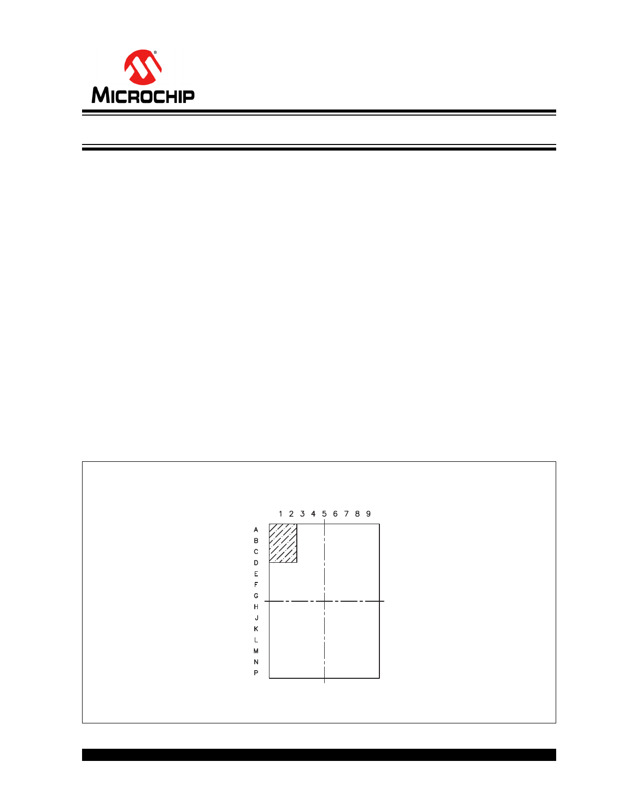
Package Type
22-lead CABGA
(Top view)
See
Table 2-1
for pad information.
High-Speed ±100V 2.5A Two-or-Three-Level Ultrasound Pulsers
HV7360/HV7361
DS20005570C-page 2
2017 Microchip Technology Inc.
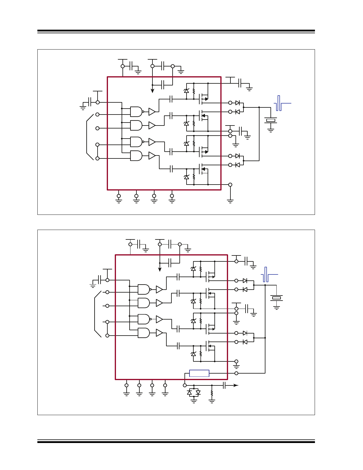
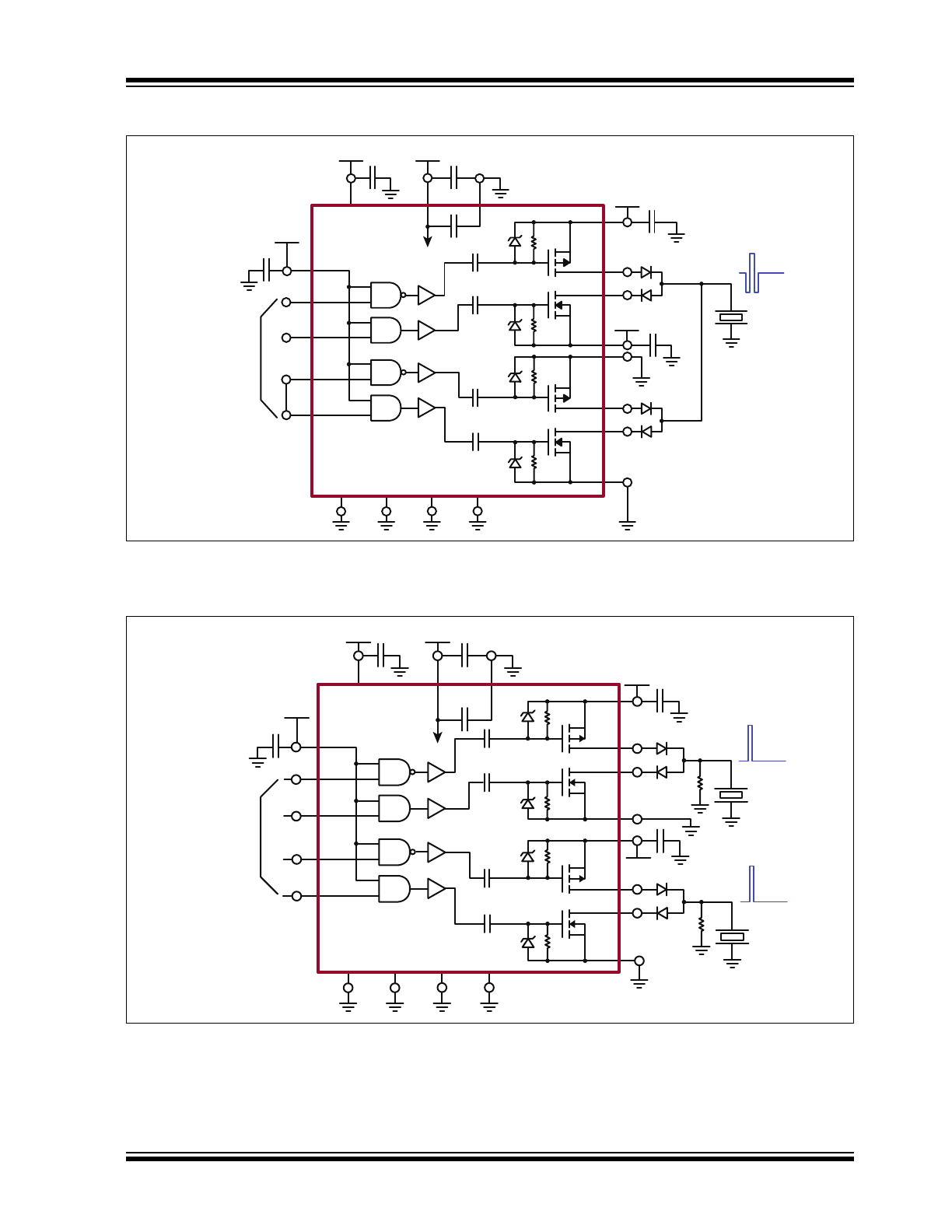
HV7360 Typical Application Circuit
HV7361 Typical Application Circuit
+/-100V 2.5A Three-level RTZ Transmit Pulsers
+2.5/3.3V V
LL
VDD
VH
INA
INB
PE
VL1
GND
INC
IND
VSS
SP1
SP2
SN1
SN2
DP1
DP2
0 to -100V
+10V
2.5/3.3V
Logic Input
DN2
DN1
VL2
VL3
+10V
HV
OUT
0 to +100V
+/-100V 2.5A Three-level RTZ Transmit Pulsers with T/R Switch
+2.5/3.3V V
LL
VDD
VH
PE
INA
INB
INC
IND
VL1
GND VSS
SP1
SP2
SN1
SN2
DP1
DP2
0 to -100V
+10V
2.5/3.3V
Logic Input
DN2
DN1
VL2
VL3
+10V
0 to +100V
T/R SW
XDCR
to Rx LNA
RX
2017 Microchip Technology Inc.
DS20005570C-page 3
HV7360/HV7361
1.0
ELECTRICAL CHARACTERISTICS
Absolute Maximum Ratings †
Chip Power Supply Voltage, V
DD
–V
SS
.................................................................................................... –0.5 to +12.5V
Output High Supply Voltage, V
H
......................................................................................................V
L
–0.5 to V
DD
+0.5V
Output Low Supply Voltage, V
L
..................................................................................................... V
SS
–0.5V to V
H
+0.5V
Low-side Supply Voltage, V
SS
.....................................................................................................................–6V to +0.5V
Differential High Voltage, V
SP1
–V
SN1
, V
SP2
–V
SN2
............................................................................................... +220V
Positive High Voltage, V
SP1,2
................................................................................................................. –0.5V to +110V
Negative High Voltage, V
SN1,2
............................................................................................................... +0.5V to –110V
All Logic Input Voltages.............................................................................................................V
SS
–0.5V to GND +5.5V
Rx to XDCR Differential Drop ............................................................................................................................... ±140V
Coupling Capacitor Breakdown Voltage................................................................................................................ ±110V
Maximum Junction Temperature, T
J
......................................................................................................................125°C
Operating Ambient Temperature, T
A
......................................................................................................–40°C to +85°C
† Notice: Stresses above those listed under “Absolute Maximum Ratings” may cause permanent damage to the
device. This is a stress rating only, and functional operation of the device at those or any other conditions above those
indicated in the operational sections of this specification is not intended. Exposure to maximum rating conditions for
extended periods may affect device reliability.
OPERATING SUPPLY VOLTAGES AND CURRENT
Electrical Specifications: GND = 0V, V
H
= V
DD
= +10V, V
L
= V
SS
= 0V, V
PE
= 3.3V, V
PP
= +100V, V
NN
= –100V,
T
A
= 25°C unless otherwise specified.
Parameter
Sym.
Min.
Typ.
Max.
Unit
Conditions
Logic Supply Voltage Range
V
LL
2.25
—
3.63
V
Supply Voltage
V
DD
-V
SS
4.75
—
11.5
V
4V ≤ V
DD
≤ 11.5V
Low Side Supply Voltage
V
SS
–5.5
—
0
V
Gate Drive High-side Voltage
V
H
V
SS
+4
—
V
DD
V
V
H
–V
L
≥ 4V
Gate Drive Low-side Voltage
V
L
V
SS
—
V
DD
–4
V
Output Positive High Voltage
V
SP1,2
0
—
100
V
Output Negative High Voltage
V
SN1,2
–100
—
0
V
V
DD
Quiescent Current
I
DDQ
—
50
—
μA
No input transitions, PE = 0
V
H
Quiescent Current
I
HQ
—
2
—
μA
V
DD
Quiescent Current
I
DDQ
—
1
—
mA
No input transitions, PE = 1
V
H
Quiescent Current
I
HQ
—
2
—
μA
V
DD
Average Current
I
DD
—
4
—
mA
One channel on at 5 MHz, no
load
V
H
Average Current
I
H
—
10
—
mA
Input Logic Voltage High
V
IH
V
PE
–0.3
—
V
PE
V
For logic inputs INA, INB, INC
and IND
Input Logic Voltage Low
V
IL
0
—
0.3
V
Input Logic Current High
I
IH
—
—
1
μA
Input Logic Current Low
I
IL
—
—
1
μA
PE Input Logic Voltage High
V
PEH
1.7
3.3
5.25
V
For logic input PE
PE Input Logic Voltage Low
V
PEL
0
—
0.3
V
PE Input Impedance to GND
R
INPE
100
—
—
kΩ
HV7360/HV7361
DS20005570C-page 4
2017 Microchip Technology Inc.
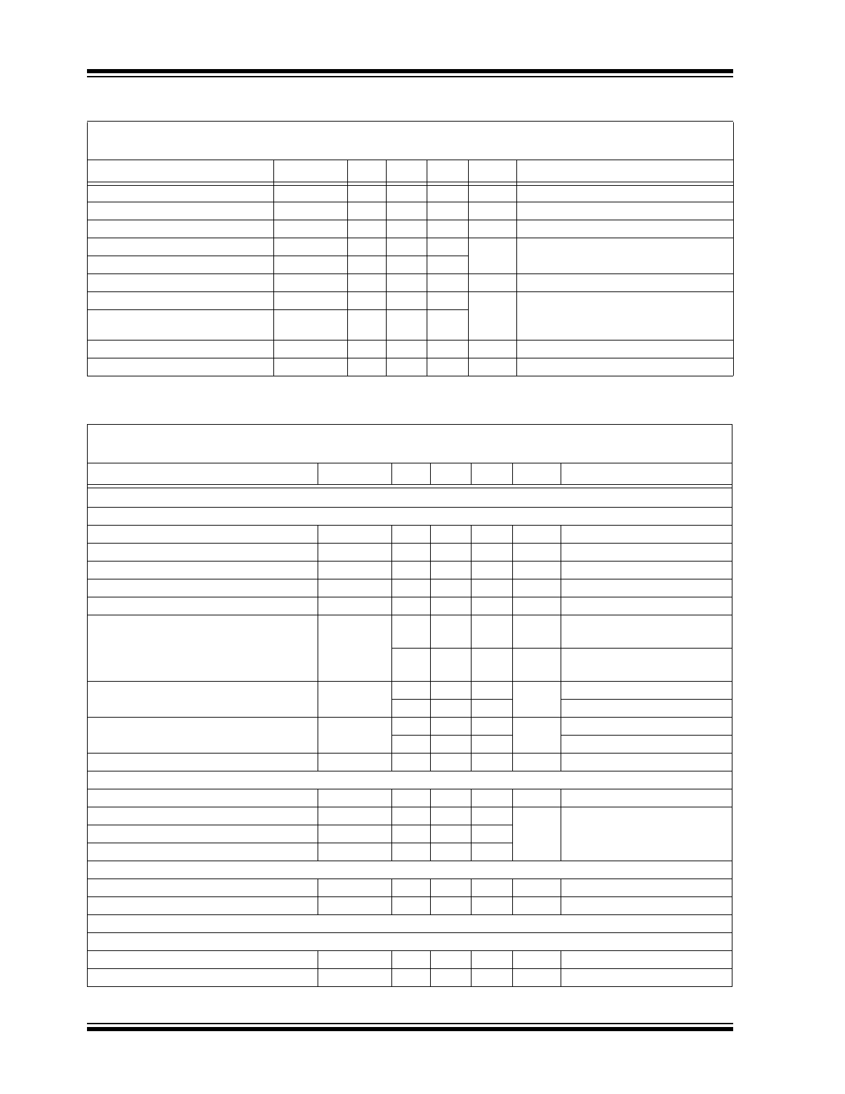
AC ELECTRICAL CHARACTERISTICS
Electrical Specifications: GND = 0V, V
H
= V
DD
= +10V, V
L
= V
SS
= 0V, V
PE
= 3.3V, V
PP
= +100V, V
NN
= –100V,
T
A
= 25°C unless otherwise specified.
Parameter
Sym.
Min.
Typ.
Max.
Unit
Conditions
Input or PE Rise and Fall Time
t
irf
—
—
10
ns
Logic input edge speed requirement
Input to Output Delay
t
d1–4
—
7.5
—
ns
R
LOAD
= 1Ω
Output Rise and Fall Time
t
r/f1–2
—
9.5
—
ns
C
LOAD
= 330 pF, R
LOAD
= 2.5 kΩ
Rise and Fall Time Matching
∆t
rf
—
2
—
ns
Channel to channel
Propagation Matching
∆t
dC2C
—
1
—
Propagation Delay Matching
∆t
dD2D
—
±2
—
ns
Device to device delay match
PE On-time
t
PE–ON
—
—
5
µs
V
PE
= 1.7 ~ 5.25V,
V
DD
= 7.5 ~ 11.5V,
–20 ~ 85°C
PE Off-time
t
PE–OFF
—
—
4
Output to MOSFET Gate Cap
C
OG
—
10
—
nF
100V X7S
V
H
to V
L3
Decoupling Cap
C
VH
—
0.22
—
µF
16V X7R
ELECTRICAL CHARACTERISTICS
Electrical Specifications: GND = 0V, V
H
= V
DD
= +10V, V
L
= V
SS
= 0V, V
PE
= 3.3V, V
PP
= +100V, V
NN
= –100V,
T
A
= 25°C unless otherwise specified.
Parameter
Sym.
Min.
Typ.
Max.
Unit
Conditions
PULSER AND DAMPING P-CHANNEL MOSFET
DC PARAMETER
Drain-to-source Breakdown Voltage
BV
DSS
–200
—
—
V
V
GS
= 0V, I
D
= –2 mA
Gate Threshold Voltage
V
GS(th)
–1
—
–2.4
V
V
GS
= V
DS
, I
D
= –1 mA
Change in V
GS(th)
with Temperature
∆V
GS(th)
—
—
4.5
mV/°C V
GS
= V
DS
, I
D
= –1 mA
Gate-to-source Shunt Resistor
R
GS
10
—
50
kΩ
I
GS
= 100 µA, if applied
Gate-to-source Zener Voltage
V
ZGS
13.2
—
25
V
I
GS
= –2 mA, if applied
Zero-gate Voltage Drain Current
I
DSS
—
—
–10
μA
V
DS
= Maximum rating,
V
GS
= 0V
—
—
–1
mA
V
DS
= 0.8 maximum rating,
V
GS
= 0V, T
A
= 125°C
ON-state Drain Current
I
D(ON)
–1.2
—
—
A
V
GS
= –5V, V
DS
= –25V
–2.3
–2.5
—
V
GS
= –10V, V
DS
= –50V
Static Drain-to-source ON-state
Resistance
R
DS(ON)
—
—
8.5
Ω
V
GS
= –5V, I
D
= –150 mA
—
—
7
V
GS
= –10V, I
D
= –1A
Change in R
DS(ON)
with Temperature
∆R
DS(ON)
—
—
1
%/°C
V
GS
= –10V, I
D
= –1 mA
AC PARAMETER
Forward Transconductance
G
FS
400
—
—
mmho V
DS
= –25V, I
D
= –500 mA
Input Capacitance
C
ISS
—
75
—
pF
V
GS
= 0V,
V
DS
= –25V,
f = 1 MHz
Common Source Output Capacitance
C
OSS
—
21
—
Reverse Transfer Capacitance
C
RSS
—
6.5
—
DIODE PARAMETER
Diode Forward Voltage Drop
V
SBD
—
—
1.8
V
V
GS
= 0V, I
SD
= 500 mA
Reverse Recovery Time of Body Diode
t
rrBD
—
300
—
ns
PULSER AND DAMPING N-CHANNEL MOSFET
DC PARAMETER
Drain-to-source Breakdown Voltage
BV
DSS
200
—
—
V
V
GS
= 0V, I
D
= 2 mA
Gate Threshold Voltage
V
GS(th)
1
—
2.4
V
V
GS
= V
DS
, I
D
= 1 mA
2017 Microchip Technology Inc.
DS20005570C-page 5
HV7360/HV7361
Change in V
GS(th)
with Temperature
∆V
GS(th)
—
—
–4.5
mV/°C V
GS
= V
DS
, I
D
= 1 mA
Gate-to-source Shunt Resistor
R
GS
10
—
50
kΩ
I
GS
= 100 µA
Gate-to-source Zener Voltage
V
ZGS
13.2
—
25
V
I
GS
= 2 mA
Zero Gate Voltage Drain Current
I
DSS
—
—
10
μA
V
DS
= Maximum rating,
V
GS
= 0V
—
—
1
mA
V
DS
= 0.8 maximum rating,
V
GS
= 0V, T
A
= 125°C
ON-state Drain Current
I
D(ON)
1.3
—
—
A
V
GS
= 5V, V
DS
= 25V
2.3
2.5
—
V
GS
= 10V, V
DS
= 50V
Static Drain-to-source ON-state
Resistance
R
DS(ON)
—
—
6.5
Ω
V
GS
= 5V, I
D
= 150 mA
—
—
6
V
GS
= 10V, I
D
= 1A
Change in R
DS(ON)
with Temperature
∆R
DS(ON)
—
—
1
%/°C
V
GS
= 10V, I
D
= 1A
AC PARAMETER
Forward Transconductance
G
FS
400
—
—
mmho V
DS
= 25V, I
D
= 500 mA
Input Capacitance
C
ISS
—
56
—
pF
V
GS
= 0V,
V
DS
= 25V,
f = 1 MHz
Common Source Output Capacitance
C
OSS
—
13
—
Reverse Transfer Capacitance
C
RSS
—
2
—
DIODE PARAMETER
Diode Forward Voltage Drop
V
SBD
—
—
1.8
V
V
GS
= 0V, I
SD
= 500 mA
Reverse Recovery Time of Body Diode
t
rrBD
—
300
—
ns
ELECTRICAL CHARACTERISTICS (CONTINUED)
Electrical Specifications: GND = 0V, V
H
= V
DD
= +10V, V
L
= V
SS
= 0V, V
PE
= 3.3V, V
PP
= +100V, V
NN
= –100V,
T
A
= 25°C unless otherwise specified.
Parameter
Sym.
Min.
Typ.
Max.
Unit
Conditions
HV7361 T/R SWITCH CHARACTERISTICS
Parameter
Sym.
Min.
Typ.
Max.
Unit
Conditions
Breakdown Voltage from XDCR to Rx
B
VA–B
±130
—
—
V
I
A–B
= ±1 mA
Switch-on Resistance from XDCR to Rx
R
SW
—
15
—
Ω
I
A–B
= ±5 mA
V
A–B
Trip Point to Turn Off
V
TRIP
—
±1
±2
V
Switch Turn-off Voltage
V
OFF
—
±2
—
V
I
A–B
= ±1 mA
Switch-off Current
I
A–B(OFF)
—
±200 ±300
µA
V
A–B
= ±130V
Peak Switching Current
I
PEAK
—
±60
—
mA
Turn-off Time
T
OFF
—
—
20
ns
Turn-on Time
T
ON
—
—
20
ns
Switch-on Capacitance from A to B or
B to A
C
SW(ON)
—
21
—
pF
SW = On
Switch-off Capacitance from A to B or
B to A
C
SW(OFF)
—
15
—
pF
V
SW
= 25V
Small Signal Bandwidth
BW
—
100
—
MHz
R
LOAD
= 50Ω
HV7360/HV7361
DS20005570C-page 6
2017 Microchip Technology Inc.
TEMPERATURE SPECIFICATIONS
Electrical Characteristics: Unless otherwise noted, for all specifications T
A
= T
J
= +25°C.
Parameter
Sym.
Min.
Typ.
Max.
Unit
Conditions
TEMPERATURE RANGE
Maximum Junction Temperature
T
J
—
—
125
°C
Operating Temperature
T
A
–40
—
+85
°C
PACKAGE THERMAL RESISTANCE
22-Lead CABGA
JA
—
106
—
°C/W
POWER-UP AND POWER-DOWN SEQUENCE
1
Power-up
Power-down
Step
Description
Step
Description
1
V
LL
1
PE inactive
2
V
DD
, V
H
, V
SS
and V
L
with signal logic low
2
V
PP
and V
NN
off
3
V
PP
and V
NN
3
V
DD
, V
H
, V
SS
and V
L
off
4
PE active
4
V
LL
off
Note 1: Powering up or down in any arbitrary sequence will not cause any damage to the device. The power-up
sequence and power-down sequence are only recommended to minimize possible inrush current.
LOGIC CONTROL TABLE
PE
Input Pulse
Output MOSFETs
INA
INB
INC
IND
SP1 to DP1 DN1 to SN1 SP2 to DP2 DN2 to SN2
1
1
X
X
X
ON
X
X
X
X
1
X
X
X
ON
X
X
X
X
1
X
X
X
ON
X
X
X
X
1
X
X
X
ON
0
X
X
X
OFF
X
X
X
X
0
X
X
X
OFF
X
X
X
X
0
X
X
X
OFF
X
X
X
X
0
X
X
X
OFF
0
X
X
X
X
OFF
OFF
OFF
OFF
2017 Microchip Technology Inc.
DS20005570C-page 7
HV7360/HV7361
2.0
PAD DESCRIPTION
Table 2-1
details the description of pads in
HV7360/HV7361. Refer to
Package Type
for the
location of pads.
TABLE 2-1:
PAD FUNCTION TABLE
Pad
Location
HV7360
Symbol
HV7361
Symbol
Description
A1
GND
GND
Driver and level translator circuit ground return (0V)
A2
IND
IND
Damping N-FET control signal logic input, controlling N-FET2
A3
INC
INC
Damping P-FET control signal logic input, controlling P-FET2
A4
V
SS
V
SS
Negative voltage power supply (0V)
A6
V
DD
V
DD
Positive voltage supply (+10V), should connect to an external decoupling cap to
V
SS
(0V)
A7
INB
INB
Pulsing N-FET control signal logic input, controlling N-FET1
A8
INA
INA
Pulsing P-FET control signal logic input, controlling P-FET1
A9
PE
PE
Drive power enable Hi = On, Low = Off, logic ‘1’ voltage reference input (+2.5V to
+3.3V)
B2
V
L2
V
L2
Gate-drive negative voltage power supply (0V)
B8
V
L1
V
L1
Gate-drive negative voltage power supply (0V)
F4
V
H
V
H
Gate-drive positive voltage power supply (+10V)
F7
V
L3
V
L3
V
H
to V
L
decoupling cap. The trace connecting V
L1
, V
L2
, and V
L3
(0V) to ground
plane should be as short as possible.
G4
NC
—
No connection for HV7360
—
RX
T/R switch output for HV7361
P1
SP2
SP2
Source of P-FET2, positive high voltage power supply (0V to +100V) or GND
P2
DP2
DP2
Drain of P-FET2, transmit pulser output
P3
DN2
DN2
Drain of N-FET2, transmit pulser output
P4
SN2
SN2
Source of N-FET2, negative high voltage power supply (0V to –100V) or GND
P5
NC
—
No connection for HV7360
—
XDCR
T/R switch input for HV7361
P6
SP1
SP1
Source of P-FET1, positive high voltage power supply (0V to +100V)
P7
DP1
DP1
Drain of P-FET1, transmit pulser output
P8
DN1
DN1
Drain of N-FET1, transmit pulser output
P9
SN1
SN1
Source of N-FET1, negative high voltage power supply (0V to –100V)
HV7360/HV7361
DS20005570C-page 8
2017 Microchip Technology Inc.
3.0
FUNCTIONAL DESCRIPTION
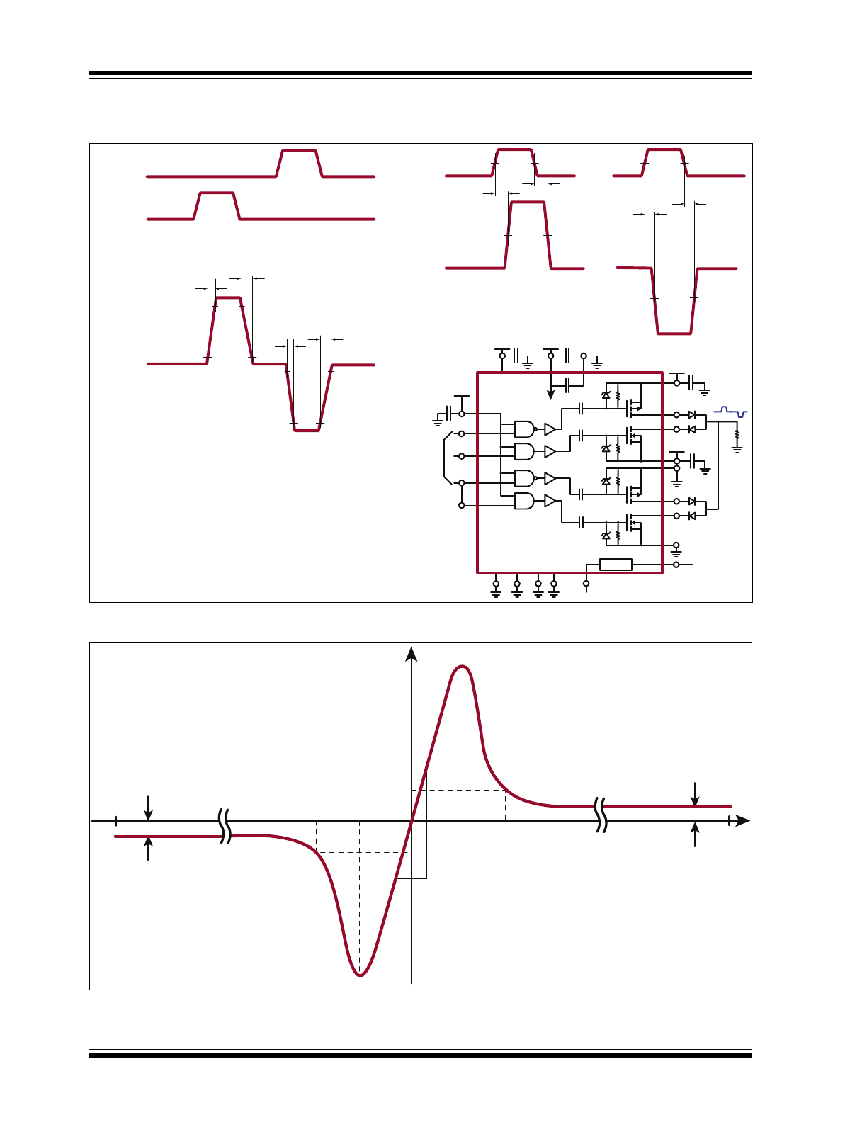
FIGURE 3-1:
Pulser Timing Test for HV7360/HV7361.
FIGURE 3-2:
T/R Switch I-V curve for HV7361.
INA
INB
TX + DMP
t
f2
50%
INA
0A
I
OUT
TX + DMP
t
r1
t
r2
t
f1
t
d1
t
d3
t
d2
t
d4
50%
50%
50%
90%
90%
10%
10%
I
OUT
INB
0A
+2.5/3.3V V
LL
VDD
VH
PE
INA
INB
INC
IND
VL1
GND VSS
SP1
DP1
DN1
SN1
SP2
DP2
DN2
SN2
XDCR
-100V
+10V
2.5/3.3V
Logic Input
VL2
VL3
+10V
+100V
T/R SW
RX
R1
I
A-B
-V
OFF
-V
TRIP
+130V
I
A-B
= -200μA
-130V
I
A-B
= +200μA
V
A-B
R
SW
= 15Ω
+I
PEAK
-I
PEAK
+V
TRIP
+V
OFF
+1.0mA
+1.0mA
2017 Microchip Technology Inc.
DS20005570C-page 9
HV7360/HV7361
FIGURE 3-3:
Typical Bipolar One-channel Three-level Ultrasound Transmitter Application Circuit for
HV7360/HV7361.
FIGURE 3-4:
Typical Unipolar Two-channel Two-level Ultrasound Transmitter Application Circuit for
HV7360/HV7361.
+2.5/3.3V V
LL
VDD
VH
INA
INB
PE
VL1
GND
INC
IND
VSS
SP1
SP2
SN1
SN2
DP1
DP2
0 to -100V
+10V
2.5/3.3V
Logic Input
DN2
DN1
VL2
VL3
+10V
HV
OUT
0 to +100V
+2.5/3.3V V
LL
VDD
VH
PE
INA
INB
INC
IND
VL1
GND
VSS
SP1
DP1
DN1
SN1
SP2
DP2
DN2
SN2
+10V
2.5/3.3V
Logic Input
VL2
VL3
+10V
0 to +100V
TX2
TX1
0 to +100V
HV7360/HV7361
DS20005570C-page 10
2017 Microchip Technology Inc.
4.0
PACKAGING INFORMATION
4.1
Package Marking Information
Legend: XX...X
Product Code or Customer-specific information
Y
Year code (last digit of calendar year)
YY
Year code (last 2 digits of calendar year)
WW
Week code (week of January 1 is week ‘01’)
NNN
Alphanumeric traceability code
Pb-free JEDEC
®
designator for Matte Tin (Sn)
*
This package is Pb-free. The Pb-free JEDEC designator ( )
can be found on the outer packaging for this package.
Note:
In the event the full Microchip part number cannot be marked on one line, it will
be carried over to the next line, thus limiting the number of available
characters for product code or customer-specific information. Package may or
not include the corporate logo.
3
e
3
e
XXXXXX
YYWWNNN
e3
XX
HV7360
e3
1724111
GA
XXXXXX
YYWWNNN
e3
XX
HV7361
e3
1718555
GA