
2015 Microchip Technology Inc.
DS20005412A-page 1
HV7351
Features
• Eight Channels with Return-to-Zero (RTZ)
• Up to ±70V Output Voltage
• ±3.0A Output Current
• Stores up to Four Different Patterns
• Independent Programmable Delays
• 80-lead Single 11 x 11 mm VQFN Package
Applications
• Medical Ultrasound Imaging
• NDT, Non-Destructive Testing
• Arbitrary Pattern Generator
• High-Speed PIN Diode Driver
General Description
The HV7351 device is an 8-channel programmable
high-voltage ultrasound-transmit beamformer. Each
channel is capable of swinging up to ±70V with an
active discharge back to 0V. The outputs can source
and sink up to 3.0A to achieve fast output rise and fall
times. The active discharge is also capable of sourcing
and sinking 3.0A for a fast return to ground. The topol-
ogy of the HV7351 will significantly reduce the number
of I/O logic control lines needed.
Each pulser has four associated 64-bit shift registers
for storing predetermined transmit patterns and a 10-bit
delay counter for controlling the transmit time. One of
four arbitrary patterns can be transmitted with adjust-
able delay, depending on the data loaded into these
shift registers and the delay counter. The delay counter
can be clocked up to 200 MHz, allowing incremental
delays down to 5 ns.
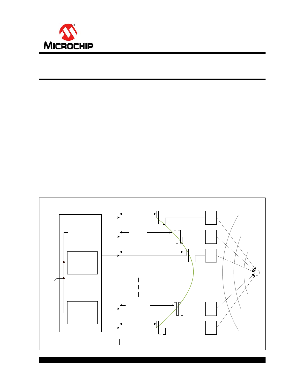
Typical Application Circuit
Tx128
TRIG
Tx127
Tx3
Tx2
Tx1
t
DELAY1
TRIG
HV7351
8-channel
U1
HV7351
8-channel
U2
HV7351
8-channel
U16
t
DELAY2
t
DELAY3
t
DELAY127
t
DELAY128
E3
E1
E2
E127
E128
Array
Probe
8-Channel, ±70V, 3A Programmable High-Voltage
Ultrasound-Transmit Beamformer
HV7351
DS20005412A-page 2
2015 Microchip Technology Inc.
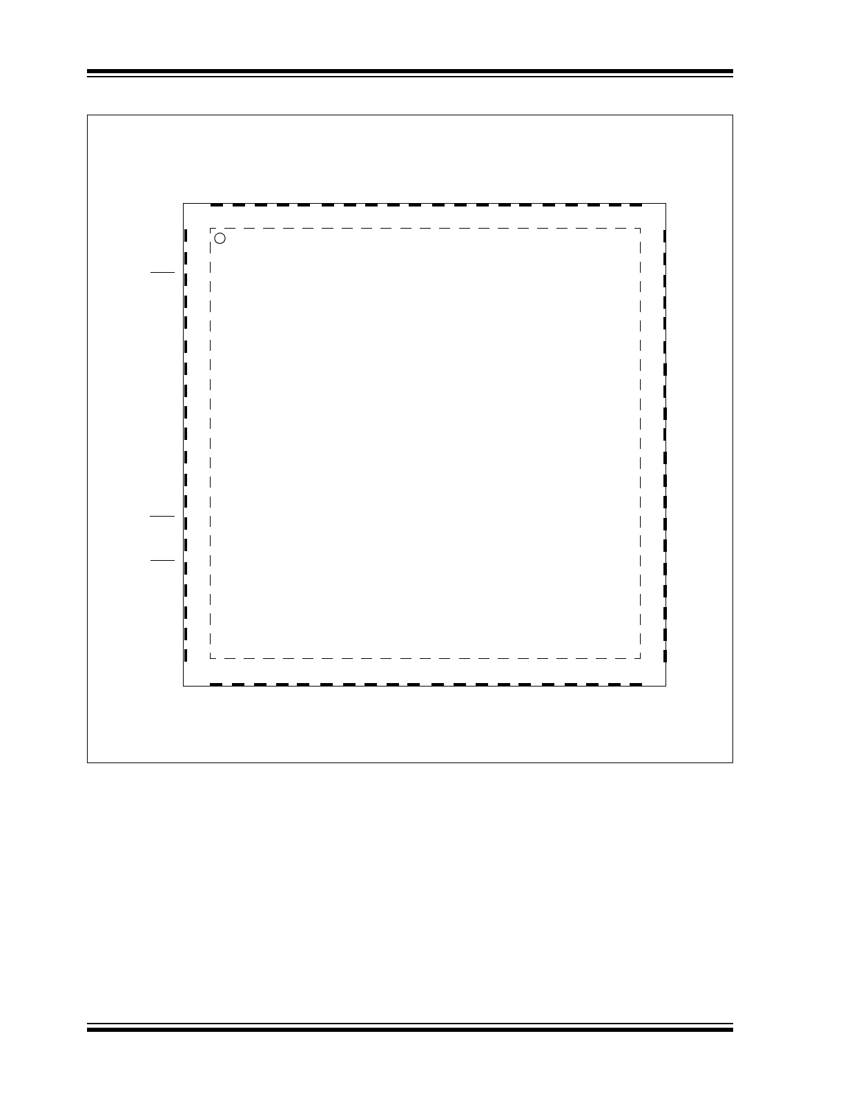
Package Types (Top View)
HV7351
11 x 11 VQFN*
DOUT2
AV
DD
INV
TCK
CS1
A0
74
71
68
65
62
80
77
81
73
70
67
64
61
79
76
72
69
66
63
78
75
27
30
33
36
39
21
24
28
31
34
37
40
22
25
29
32
35
38
23
26
7
10
13
16
19
1
4
8
11
14
17
20
2
5
9
12
15
18
3
6
54
51
48
45
42
60
57
53
50
47
44
41
59
56
52
49
46
43
58
55
DIN2
SIZE
DV
DD
SCK
EN
CW
CS2
D
GND
TRIG
TCK
V
LL
DOUT1
DIN1
A1
PV
SS
V
NN
V
PF
P
GND
V
PF
D
GND
V
NF
V
PP
PV
DD
P
GND
P
GND
D
GND
DV
DD
PV
SS
P
GND
V
NN
V
NF
D
GND
PV
DD
V
PP
NC
V
RN
PV
SS
TX2
TX3
V
PP
PV
DD
P
GN
D
TX1
V
NN
V
NF
V
PF
P
GN
D
V
PP
V
PP
V
NN
V
NN
V
PP
V
NN
TX4
NC
V
RP
PV
SS
TX7
TX6
V
PP
PV
DD
P
GN
D
TX8
V
NN
V
NF
V
PF
P
GN
D
V
PP
V
PP
V
NN
V
NN
V
PP
V
NN
TX5
V
SUB
* Includes Exposed Thermal Pad (EP); see
Table 2-1
.
2015 Microchip Technology Inc.
DS20005412A-page 3
HV7351
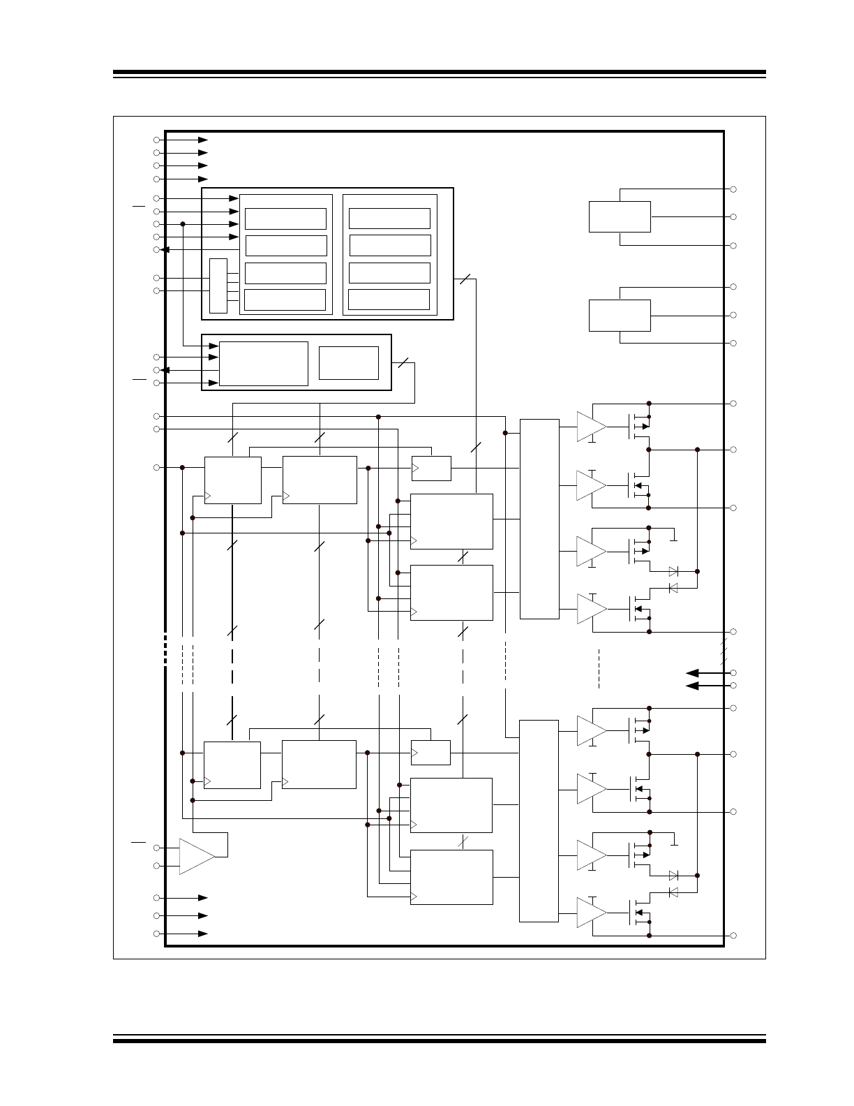
Block Diagram
INV
EN/LD
CW
CLK
16/32 bit
Serial
Shift Reg.
INV
EN/LD
CW
CLK
16/32 bit
Serial
Shift Reg.
INV
EN/LD
CW
CLK
16/32 bit
Serial
Shift Reg.
INV
EN/LD
CW
CLK
16/32 bit
Serial
Shift Reg.
Divide
by 2
6-bit Counter
Divide by N
N = 1 to 64
Linear
Regulator
Linear
Regulator
EN
EN
10-bit Delay
Counter
Divide
by 2
V
LL
to V
DD
Translator
-
+
P
GND
P
GND
V
PF
V
PF
V
NF
V
NF
PV
SS
PV
DD
PV
SS
PV
DD
V
PP
V
PF
V
RN
V
RP
V
NF
V
NN
V
PP
TX1
V
NN
P
GND
PV
DD
PV
SS
V
PP
TX8
V
NN
P
GND
CW
f
CW
PIN
NIN
Control
Logic
CW
f
CW
PIN
NIN
Control
Logic
RTZ GATE Driver
Supply Voltages
6-bit Counter
Divide by N
N = 1 to 64
EN
EN
10-bit Delay
Counter
8 10-bit Registers
for Delay Counters
6-bit for
Divide by N
16/32-bit Register
Pattern 4
16/32-bit Register
Pattern 3
16/32-bit Register
Pattern 2
16/32-bit Register
Pattern 1
16/32-bit Register
Pattern 4
16/32-bit Register
Pattern 3
16/32-bit Register
Pattern 2
16/32-bit Register
Pattern 1
P-Ch. Registers
N-Ch. Registers
Decoder
V
PF
V
RN
V
PP
V
NF
V
NN
V
RP
V
LL
AV
DD
DV
DD
EN
SIZE
SCK
DIN1
DOUT1
A0
A1
DIN2
DOUT2
CW
INV
TRIG
TCK
D
GND
A
GND
V
SUB
CS2
CS1
TCK

HV7351
DS20005412A-page 4
2015 Microchip Technology Inc.
NOTES:
2015 Microchip Technology Inc.
DS20005412A-page 5
HV7351
1.0
ELECTRICAL
CHARACTERISTICS
Absolute Maximum Ratings †
Positive logic supply (V
LL
)............................................................................................................................ -0.5V to 5.5V
Positive logic supply voltage (DV
DD
)............................................................................................................ -0.5V to 5.5V
Positive gate drive supply voltage (PV
DD
) ................................................................................................... -0.5V to 5.5V
Positive analog supply voltage (AV
DD
)......................................................................................................... -0.5V to 5.5V
Negative gate drive supply voltage (PV
SS
) ................................................................................................ +0.5V to -5.5V
High-voltage positive supply voltage (V
PP
) ................................................................................................. -0.5V to +80V
High-voltage negative supply voltage (V
NN
) ............................................................................................... +0.5V to -80V
Differential high voltage supply (V
PP
- V
NN
) ............................................................................................................+160V
Positive floating supply voltage (V
PF
) .................................................................................................. V
PP
– 6.0V to V
PP
Negative floating supply voltage (V
NF
)................................................................................................. V
NN
to V
NN
+ 6.0V
Positive supply for V
NF
regulator (V
RP
)............................................................................................................. 0V to 15V
Negative supply for V
PF
regulator (V
RN
) .......................................................................................................... 0V to -15V
Operating temperature ........................................................................................................................... -40°C to +125°C
Storage temperature ............................................................................................................................... -65°C to +150°C
ESD Rating All Pins .............................................................................................................................................. 0.75 kV
† Notice: Stresses above those listed under “Maximum Ratings” may cause permanent damage to the device. This is
a stress rating only and functional operation of the device at those or any other conditions above those indicated in the
operational sections of this specification is not intended. Exposure to maximum rating conditions for extended periods
may affect device reliability.
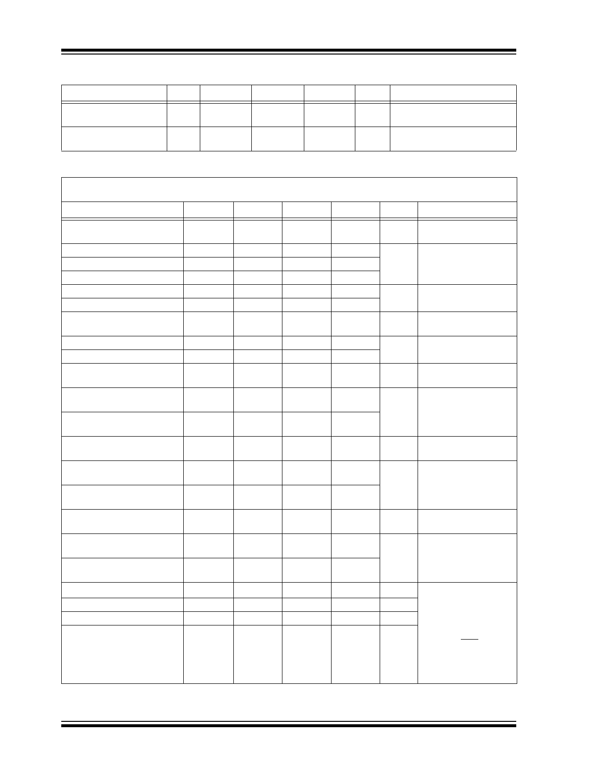
TABLE 1-1:
OPERATING SUPPLY VOLTAGES
Electrical Specifications: Unless otherwise specified: T
A
= +25°C. Boldface specifications apply over the T
A
range
of -20 to +85°C.
Parameter
Sym.
Min.
Typ.
Max.
Units
Conditions
Positive High Voltage Supply
V
PP
3.0
—
70
V
Note 1
Negative High Voltage Supply
V
NN
-70
—
-3.0
V
Logic Interface Voltage
V
LL
2.85
3.30
3.6
V
Low-Voltage Positive Analog
Supply Voltage
AV
DD
4.75
5.00
5.25
V
Low-Voltage Positive Digital
Supply Voltage
DV
DD
4.75
5.00
5.25
V
Low-Voltage Positive Gate Drive
Supply Voltage
PV
DD
4.75
5.00
5.25
V
Low-Voltage Negative Gate
Drive Supply Voltage
PV
SS
-5.25
-5.00
-4.75
V
Low-Voltage Positive Supply
for V
NF
Regulator
V
RP
4.75
—
12
V
Low-Voltage Negative Supply
for V
PF
Regulator
V
RN
-12
—
-4.75
V
Reference Voltage Logic Trip
Point for TCK Pin
TCK
0.4V
LL
0.5V
LL
0.6V
LL
V
TCK/TCK Input Current
I
TCK
/I
TCK
—
—
±10
µA
I
TCK
= 0 to V
LL
,
T
A
= +25°C
(
Note 1
)
Note 1:
Specification is obtained by characterization and is not 100% tested.
HV7351
DS20005412A-page 6
2015 Microchip Technology Inc.
TABLE 1-2:
REGULATOR OUTPUTS
Parameter
Sym.
Min.
Typ.
Max.
Units
Conditions
Positive Floating Gate
Drive Voltage
V
PF
V
PP
- 5.25
V
PP
- 5.00
V
PP
- 4.00
V
4x1 µF ceramic capacitors
across V
PF
and V
PP
Negative Floating Gate
Drive Voltage
V
NF
V
NN
+ 4.00
V
NN
+ 5.00
V
NN
+ 5.25
V
4x1 µF ceramic capacitors
across V
NF
and V
NN
ELECTRICAL CHARACTERISTICS
Electrical Specifications: unless otherwise specified, V
LL
= 3.3V, AV
DD
= DV
DD
= PV
DD
= V
RP
= 5.0V,
PV
SS
= V
RN
= -5.0V, V
PP
= +70V, V
NN
= -70V, T
A
= +25°C.
Parameter
Sym.
Min.
Typ.
Max.
Units
Conditions
V
LL
Quiescent Current
I
VLLQ
—
384
500
µA
EN = Low,
all inputs are static
AV
DD
Quiescent Current
I
AVDDQ
—
12
30
µA
EN = Low,
all inputs are static
DV
DD
Quiescent Current
I
DVDDQ
—
12
30
PV
DD
Quiescent Current
I
PVDDQ
—
70
100
V
RP
Quiescent Current
I
VRPQ
—
0.3
6
µA
EN = Low,
all inputs are static
V
RN
Quiescent Current
I
VRNQ
—
-0.01
6
PV
SS
Quiescent Current
I
PVSSQ
-85
-45
—
µA
EN = Low,
all inputs are static
V
PP
Quiescent Current
I
VPPQ
—
2.6
6
µA
EN = Low,
all inputs are static
V
NN
Quiescent Current
I
VNNQ
—
-1.6
6
V
LL
Enabled
Quiescent Current
I
VLLEN
—
390
500
µA
EN = High,
all inputs are static
AV
DD
Enabled
Quiescent Current
I
AVDDEN
—
600
800
µA
EN = High,
all inputs are static
DV
DD
Enabled
Quiescent Current
I
DVDDEN
—
22
55
PV
DD
Enabled
Quiescent Current
I
PVDDEN
—
44
100
µA
EN = High,
all inputs are static
V
RP
Enabled
Quiescent Current
I
VRPEN
—
450
650
µA
EN = High,
all inputs are static
V
RN
Enabled
Quiescent Current
I
VRNEN
-650
-350
—
PV
SS
Enabled
Quiescent Current
I
PVSSEN
-100
-44
—
µA
EN = High,
all inputs are static
V
PP
Enabled
Quiescent Current
I
VPPEN
—
370
620
µA
EN = High,
all inputs are static
V
NN
Enabled
Quiescent Current
I
VNNEN
-620
-420
—
V
LL
current at 80 MHz Clock
I
VLLCW
—
500
—
µA
V
PP
= +5.0V,
V
NN
= -5.0V,
EN = High,
CW = High,
80 MHz on TCK,
0.5V
LL
on TCK,
all 8 channels active at
5.0 MHz, no load
(
Note 1
)
DV
DD
current at CW = 5 MHz
I
DVDDCW
—
25
—
mA
V
PP
current at CW = 5 MHz
I
VPPCW
—
141
—
mA
V
NN
current at CW = 5 MHz
I
VNNCW
—
98
—
mA
Note 1:
Specification is obtained by characterization and is not 100% tested.
2015 Microchip Technology Inc.
DS20005412A-page 7
HV7351
AC ELECTRICAL CHARACTERISTICS
Electrical Specifications: unless otherwise specified, V
LL
= 3.3V, AV
DD
= DV
DD
= PV
DD
= V
RP
= 5.0V,
PV
SS
= V
RN
= -5.0V, V
PP
= +70V, V
NN
= -70V, T
A
= +25°C.
Parameter
Sym. Min.
Typ.
Max.
Units
Conditions
Transmit Clock
Frequency
f
TCK
0
—
200
MHz
Serial Clock Frequency
f
SCK
0
—
80
MHz
No daisy chain
0
—
70
Daisy chained (
Note 2
)
Set-up Time Data
into SCK
t
SU-DIN
2
—
—
ns
Note 1
Hold Time SCK
to Data In
t
H-DIN
2
—
—
ns
Note 1
Set-up Time CS1 Low
to SCK
t
SU-CS1
2
—
—
ns
Note 2
Set-up Time CS2 Low
to SCK
t
SU-CS2
2
—
—
ns
Note 2
Set-up Time from TRIG
Fall to TCK Rise Edge
t
SU-TRIG
2
—
—
ns
Note 2
TRIG Pulse Width
t
W-TRIG
2 x TCK
—
—
Cycle
Note 2
SCK to Data Out Low
to High Delay Time
t
LHDO
3
9
12
ns
For DOUT1 (
Note 1
)
3
9
10
For DOUT2 (
Note 1
)
SCK to Data Out High
to Low Delay Time
t
HLDO
3
9
12
ns
For DOUT1 (
Note 1
)
3
9
10
For DOUT2 (
Note 1
)
A1A0 Pulse Width
t
WA1A0
t
W-TRIG
+ 40
—
—
ns
Note 2
Set-up Time A1A0 to
TRIG Rising Edge
t
SUA1A0
—
20
—
ns
Note 1
Hold Time A1A0 to
TRIG Falling Edge
t
HA1A0
—
20
—
ns
Device Enable Time
t
EN-ON
—
1
—
ms
1.0 µF capacitor on every
V
PF
and V
NF
pin (
Note 1
)
Device Disable Time
t
EN-OFF
—
—
100
ns
Note 1
Output Rise Time
from 0V to +HV
t
r1
—
9
13
ns
Load = 330 pF||2.5 k
Output Fall Time
from 0V to -HV
t
f1
—
9
13
ns
Damping Output Rise
Time from -HV to 0V
t
r2
—
9
13
ns
Damping Output Fall
Time from +HV to 0V
t
f2
—
9
13
ns
Output Rise Time from
-HV to +HV
t
r3
—
17
23
ns
Output Fall Time from
+HV to -HV
t
f3
—
17
23
ns
CW Output Rise Time
t
rcw
—
9
16
ns
V
PP
= +5.0V,
V
NN
= -5.0V
Load = 330 pF||2.5 k
CW Output Fall Time
t
fcw
—
9
16
ns
Note 1:
Specification is obtained by characterization and is not 100% tested.
2:
Specification is for design guidance only.
HV7351
DS20005412A-page 8
2015 Microchip Technology Inc.
Output Propagation
Delay Rise Time 1
t
dr1
11
14
18
ns
No Load
Output Propagation
Delay Fall Time 1
t
df1
11
14
18
ns
Output Propagation
Delay Rise Time 2
t
dr2
12
15
19
ns
Output Propagation
Delay Fall Time 2
t
df2
11
15
18
ns
Output Propagation
Delay Rise Time 3
t
dr3
12
15
19
ns
Output Propagation
Delay Fall Time 3
t
df3
11
15
18
ns
CW Output
Propagation Delay
Time from Low to High
t
dcwlh
10
13
17
ns
V
PP
= +5.0V,
V
NN
= -5.0V
No Load
CW Output
Propagation Delay
Time from High to Low
t
dcwhl
10
14
17
ns
Delay Time Matching
t
dcwhl
—
±0.7
—
ns
P to N,
channel-to-channel
matching
Delay Jitter On Rise
or Fall
t
JCW
—
13
—
ps
V
PP
= +5.0V, V
NN
= -5.0V,
Load = 50
Note 2
Latency
LAT
3.5
TCK
Note 2
Output P-Channel MOSFET to V
PP
, CW = 0
Output
Saturation Current
I
OUT
2.2
3.2
—
A
Output ON-Resistance
R
ON
—
4.2
—
I
OUT
= 100 mA
Output Capacitance
C
OSS
—
62
—
pF
V
PP
- V
OUT
= 25V,
f = 1.0 MHz (
Note 2
)
Output N-Channel MOSFET to V
NN
, CW = 0
Output
Saturation Current
I
OUT
2.2
3.2
—
A
Output ON-Resistance
R
ON
—
2.4
—
I
OUT
= -100 mA
Output Capacitance
C
OSS
—
50
—
pF
V
NN
- V
OUT
= -25V,
f = 1.0 MHz (
Note 2
)
Output P-Channel MOSFET to V
PP
, CW = 1
Output
Saturation Current
I
OUT
1.2
1.5
—
A
Output ON-Resistance
R
ON
—
8
—
I
OUT
= 100 mA
Output Capacitance
C
OSS
—
62
—
pF
V
PP
- V
OUT
= 25V,
f = 1.0 MHz (
Note 2
)
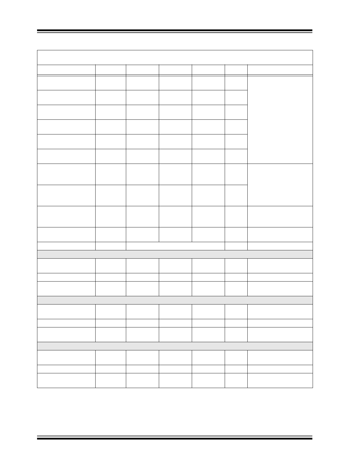
AC ELECTRICAL CHARACTERISTICS (CONTINUED)
Electrical Specifications: unless otherwise specified, V
LL
= 3.3V, AV
DD
= DV
DD
= PV
DD
= V
RP
= 5.0V,
PV
SS
= V
RN
= -5.0V, V
PP
= +70V, V
NN
= -70V, T
A
= +25°C.
Parameter
Sym. Min.
Typ.
Max.
Units
Conditions
Note 1:
Specification is obtained by characterization and is not 100% tested.
2:
Specification is for design guidance only.
2015 Microchip Technology Inc.
DS20005412A-page 9
HV7351
Output N-Channel MOSFET to V
NN
, CW = 1
Output
Saturation Current
I
OUT
1.2
1.5
—
A
Output ON-Resistance
R
ON
—
6.6
—
I
OUT
= -100 mA
Output Capacitance
C
OSS
—
50
—
pF
V
NN
- V
OUT
= -25V,
f = 1.0 MHz (
Note 2
)
Damping P-Channel MOSFET to P
GND
Output
Saturation Current
I
OUT
2.2
3.2
—
A
Output ON-Resistance
R
ON
—
4
—
I
OUT
= 100 mA
Output capacitance
C
OSS
—
62
—
pF
V
PP
- V
OUT
= 25V,
f = 1.0 MHz (
Note 2
)
Damping N-Channel MOSFET to P
GND
Output
Saturation Current
I
OUT
2.2
3.2
—
A
Output ON-Resistance
R
ON
—
2.3
—
I
OUT
= -100 mA
Output Capacitance
C
OSS
—
50
—
pF
V
NN
- V
OUT
= -25V,
f = 1.0 MHz (
Note 2
)
Logic Inputs
Clock Input Current
I
TCK
—
±1.0
—
µA
Voltage 0 to V
LL
Clock Input
High Voltage
V
IH_TCK
V
TCK
+ 0.15
—
V
LL
V
TCK = 0.5V
LL
(
Note 2
)
Clock Input
Low Voltage
V
IL_TCK
0
—
V
TCK
- 0.15
V
Logic Input
High Voltage
V
IH
0.8V
LL
—
V
LL
V
For all logic inputs except
clock inputs
Logic Input
Low Voltage
V
IL
0
—
0.2V
LL
V
Input Logic
High Current
I
IH
—
—
1
µA
Input Logic
Low Current
I
IL
-1
—
—
µA
Output Logic
Low Voltage
V
OL
0
—
0.7
V
I
OUT
= 0 to -10 mA
Output Logic
High Voltage
V
OH
V
LL
- 0.7
—
V
LL
V
I
OUT
= 0 to 10 mA
Input Logic
Capacitance
C
IN
—
—
5.0
pF
Note 2
AC ELECTRICAL CHARACTERISTICS (CONTINUED)
Electrical Specifications: unless otherwise specified, V
LL
= 3.3V, AV
DD
= DV
DD
= PV
DD
= V
RP
= 5.0V,
PV
SS
= V
RN
= -5.0V, V
PP
= +70V, V
NN
= -70V, T
A
= +25°C.
Parameter
Sym. Min.
Typ.
Max.
Units
Conditions
Note 1:
Specification is obtained by characterization and is not 100% tested.
2:
Specification is for design guidance only.
HV7351
DS20005412A-page 10
2015 Microchip Technology Inc.
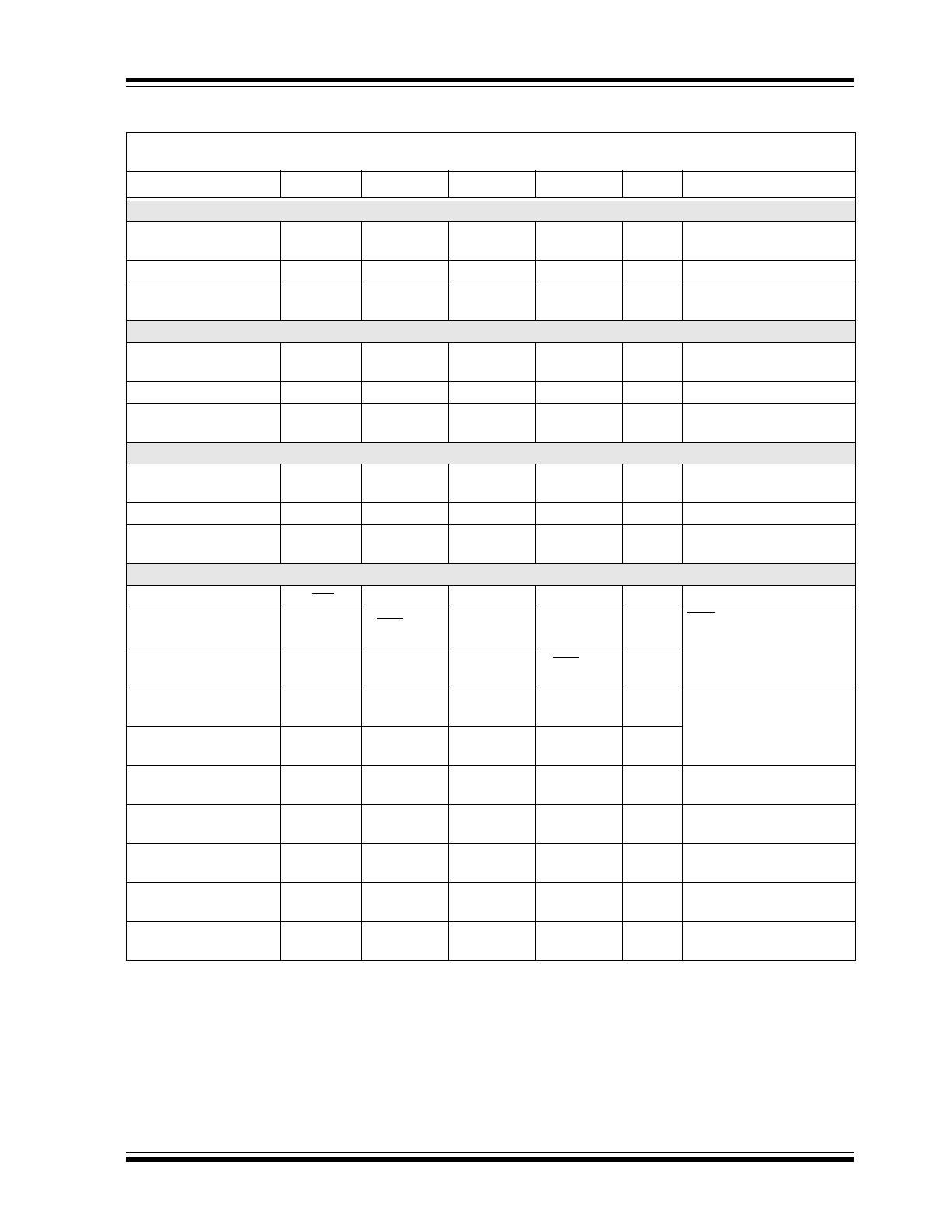
TEMPERATURE SPECIFICATIONS
Electrical Specifications: unless otherwise specified, V
LL
= 3.3V, AV
DD
= DV
DD
= PV
DD
= V
RP
= 5.0V,
PV
SS
= V
RN
= -5.0V, V
PP
= +70V, V
NN
= -70V, T
A
= +25°C.
Parameters
Sym.
Min.
Typ.
Max.
Units
Conditions
Temperature Ranges
Operating Ambient Temperature Range
T
A
-40
—
+125
°C
Storage Temperature Range
T
A
-65
—
+150
°C
Maximum Junction Temperature
T
J
-40
—
+150
°C
Package Thermal Resistances
Thermal Resistance, 80L-11x11 VQFN
JA
—
14
—
°C/W
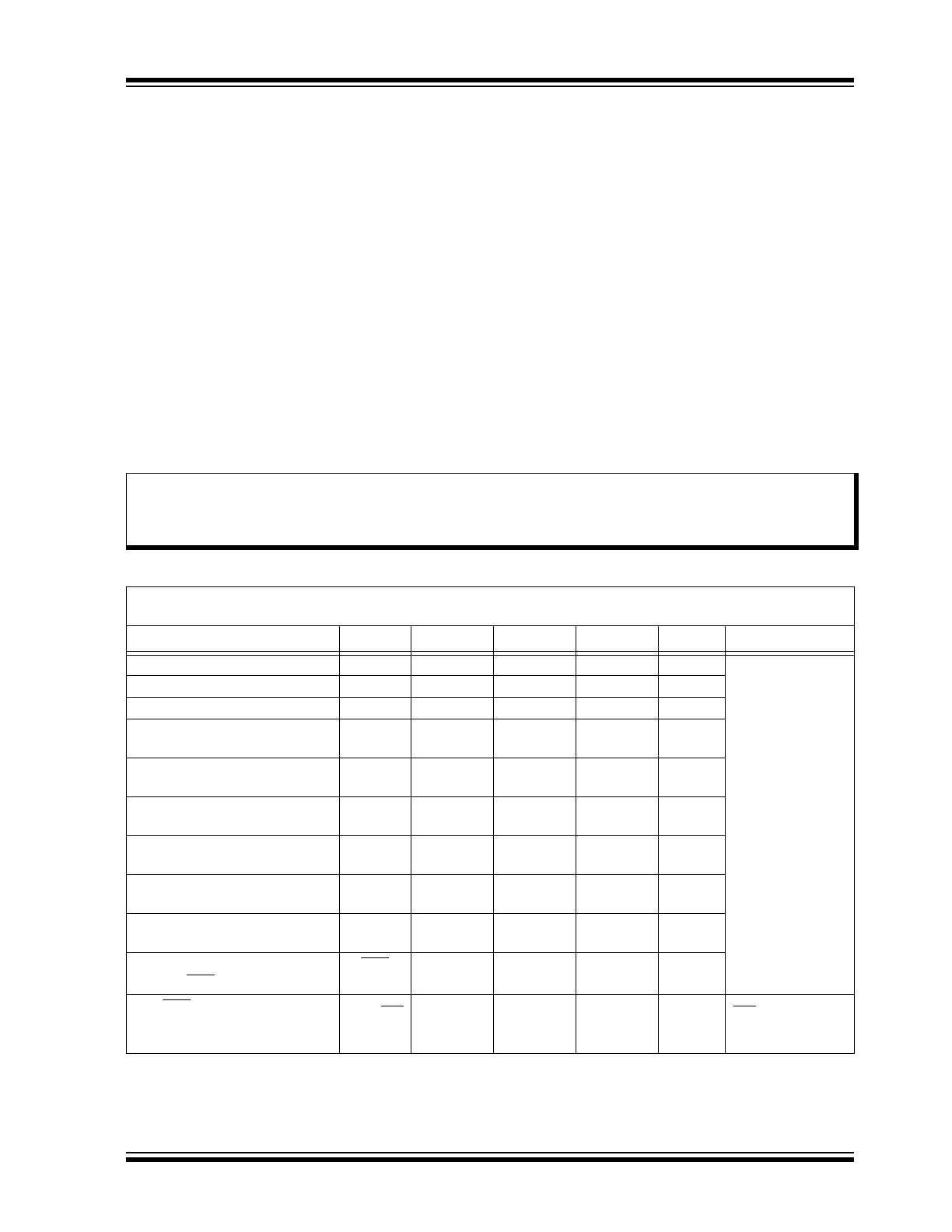
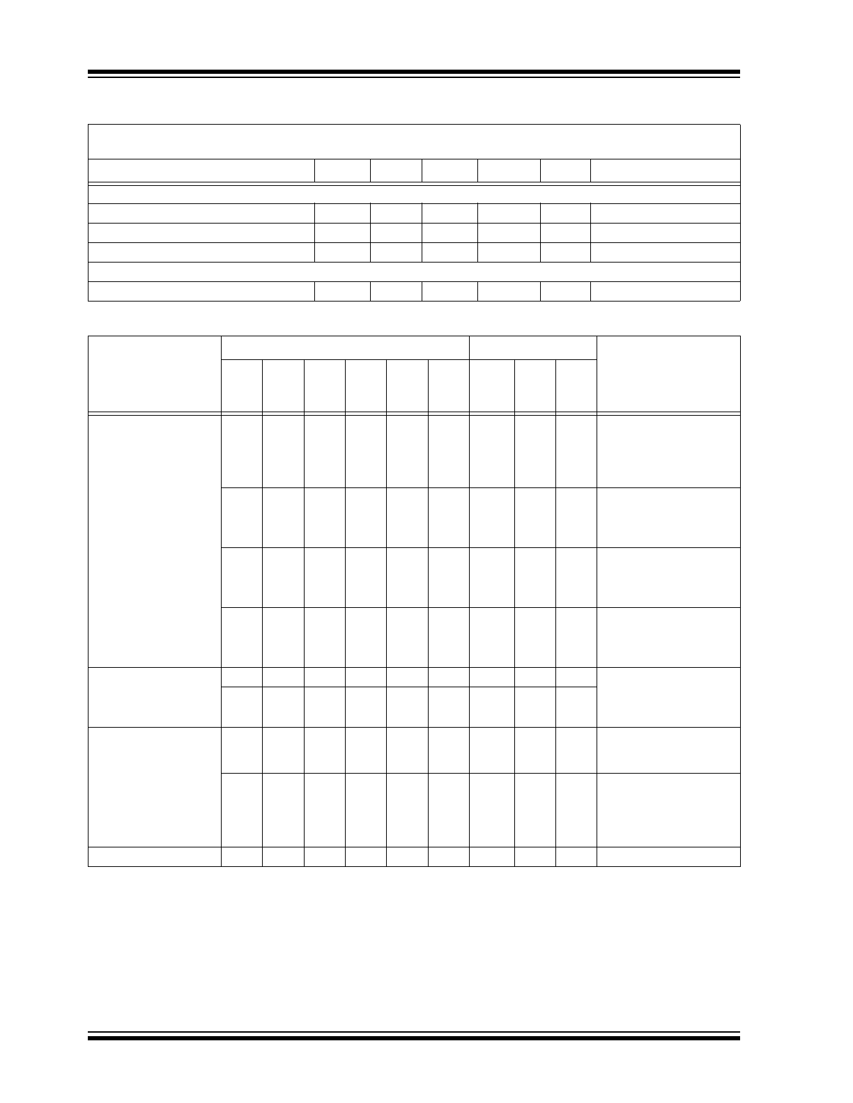
TABLE 1-3:
LOGIC TRUTH TABLE
Mode
Inputs
Outputs
Comments
EN
CW
10-b
it
Co
u
n
ter
INV
NIN
PIN
N-Ch.
P-Ch. RTZ
Non-CW mode. Outputs
not inverted. Outputs are
controlled by data in the
shift registers
1
0
X
X
0
0
OFF
OFF
ON
Return-to-Zero (RTZ) is
activated when NIN and
PIN are both low. Output is
pulled to ground through a
series diode.
1
0
X
0
0
1
OFF
ON
OFF
Not inverted. Logic
1
in the
P-Channel register turns
on the output P-Channel
MOSFET.
1
0
X
0
1
0
ON
OFF
OFF
Not inverted. Logic
1
in the
N-Channel register turns
on the output N-Channel
MOSFET.
1
0
X
X
1
1
OFF
OFF
OFF
Avoids cross overcurrent.
A logic 1 in both P- and N-
Channel registers will put
the output in a High Z state.
Non-CW mode. Outputs
are inverted. Outputs are
controlled by data in the
shift registers
1
0
X
1
0
1
ON
OFF
OFF
Transmit pattern is inverted
1
0
X
1
1
0
OFF
ON
OFF
CW mode.
Output follows f
CW
1
X
All
1
X
X
X
OFF
OFF
OFF
If 10-bit counter reach all
1
,
then the channel will be
turned OFF.
1
1
Not
all
1
X
X
X
OFF/
ON
ON/
OFF
OFF
The channel's output fol-
lows the f
CW
signal. The
shift registers for PIN and
NIN remain static to save
power.
Device Disabled
0
X
X
X
X
X
OFF
OFF
OFF
High Z state
Legend: X = Don’t care.