
2016 Microchip Technology Inc.
DS20005627A-page 1
HV7350
Features
• HVCMOS
®
Technology for High Performance
• High-density Integrated Ultrasound Transmitter
• 0V to ±60V Output Voltage
• ±1A Source and Sink Current in Pulse Mode
• ±1A Source and Sink Current in Return-to-Zero
(RTZ) Mode
• Up to 20 MHz Operating Frequency
• Matched Delay Times
• Optional Clock Realignment
• 3.3V CMOS Logic Interface and Reference
• +3.3V Low-voltage Supply for V
DD
• Built-in Linear Regulators for Floating Gate
Drivers
• Built-in Output Drain Diodes and Bleed Resistors
Applications
• Portable Medical Ultrasound Imaging
• Piezoelectric Transducer Drivers
• Pulse Waveform Generator
General Description
The HV7350 is an 8-channel monolithic high-voltage
high-speed pulse generator with built-in fast return to
zero-damping FETs. This high-voltage and high-speed
integrated circuit is designed for portable medical
ultrasound imaging system.
The HV7350 consists of a controller logic interface
circuit, level translators, MOSFET gate drives, and
high-current power P-channel and N-channel
MOSFETs as the output stage for each channel.
The output peak currents of each channel are
guaranteed to be over ±1A with up to ±60V pulse
swings as well as Return-to-Zero mode. The gate
drivers for the output MOSFETs are powered by built-in
linear 5V regulators referenced to V
PP
and V
NN
. This
direct coupling topology of the gate drivers not only
saves four floating voltage supplies or AC coupling
capacitors per channel but also makes the PCB layout
smaller and easier.
An input clock pin is available to realign all the logic
input control lines to a master clock. Precise logic
timing is always essential in any ultrasound systems.
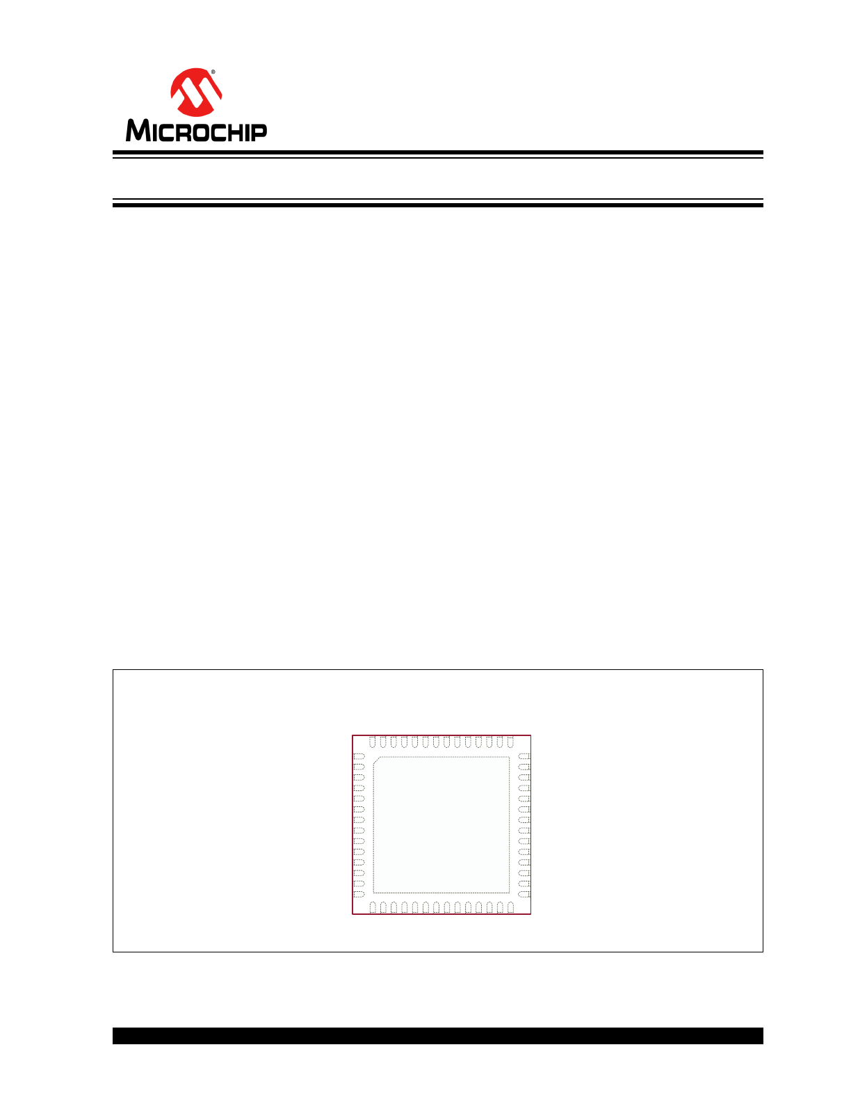
Package Type
56-lead (8 X 8) QFN
(Top view)
See
Table 2-1
for pin information.
1
56
8-Channel High-Speed ±60V ±1A Ultrasound RTZ Pulser
HV7350
DS20005627A-page 2
2016 Microchip Technology Inc.
Typical Application Circuit
CPF
VDD
+3.3V
3.3V Logic
RGND
HV
OUT
1
X1
VPP
+10 to +60V
-10 to -60V
P-Driver
N-Driver
1 of 8 Channels
Logic
&
Level
Translator
-5.0V
RGND
RGND
DMP
1.0µF
VPF
VNF
Rb
LRP
CPOS
GND
GND
SUB
REN
OEN
PIN1
NIN1
PIN8
NIN8
CLK
DAP
LRP
GND
LRN
GND
VNF
VPF
LRN
GND
GND
CNEG
CNF
VNN
+5.0V
-5.0V
1.0µF
1.0µF
1.0µF
1.0µF
TX1
1.0µF
1.0µF
VLL
+3.3V
0.1µF
+5.0V
2016 Microchip Technology Inc.
DS20005627A-page 3
HV7350
1.0
ELECTRICAL CHARACTERISTICS
Absolute Maximum Ratings †
GND and Substrate Voltage, VSUB ........................................................................................................................... 0V
Positive Logic Supply, V
LL
.......................................................................................................................–0.5V to +5.5V
Positive Logic and Level Translator Supply, V
DD
....................................................................................–0.5V to +5.5V
Positive Level Translator Decoupling Pin, C
POS
to GND ........................................................................–0.5V to +5.5V
Negative Level Translator Decoupling Pin, C
NEG
to GND ......................................................................+0.5V to –5.5V
Positive Floating Gate Driver Decoupling Pin, V
PP
–C
PF
..........................................................................–0.5V to +5.5V
Floating Gate Driver Decoupling Pin, C
NF
–V
NN
.......................................................................................–0.5V to +5.5V
Differential High-voltage Supply, V
PP
–V
NN
........................................................................................................... +130V
High-voltage Positive Supply, V
PP
............................................................................................................–0.5V to +65V
High-voltage Negative Supply, V
NN
.........................................................................................................+0.5V to –65V
All Logic Input CLK, PIN
X
, NIN
X
, OEN and REN Voltages ......................................................................–0.5V to +5.5V
Operating Junction Temperature, T
J
.....................................................................................................–40°C to +125°C
Storage Temperature, T
S
......................................................................................................................–65°C to +150°C
ESD Rating (
Note 1
).................................................................................................................................ESD Sensitive
† Notice: Stresses above those listed under “Absolute Maximum Ratings” may cause permanent damage to the
device. This is a stress rating only, and functional operation of the device at those or any other conditions above those
indicated in the operational sections of this specification is not intended. Exposure to maximum rating conditions for
extended periods may affect device reliability.
Note 1: Devices are ESD sensitive. Handling precautions are recommended.
OPERATING SUPPLY VOLTAGES AND CURRENT
(EIGHT ACTIVE CHANNELS)
Electrical Specifications: V
LL
= +3.3V, V
DD
= +3.3V, V
PP
= +60V, V
NN
= –60V, V
CLK
= +3.3V, T
A
= 25°C unless
otherwise indicated.
Parameter
Sym.
Min.
Typ.
Max.
Unit
Conditions
V
DD
Voltage Supply
V
DD
2.97
3.3
5.2
V
V
DD
UVLO
UVLO
DD
2.3
2.6
2.8
V
Logic Voltage Reference
V
LL
2.5
3.3
5
V
V
LL
UVLO
UVLO
LL
1.3
1.55
1.7
V
Positive High-voltage Supply
V
PP
+10
—
+60
V
Negative High-voltage Supply
V
NN
–60
—
–10
V
V
LL
Current
I
LLQ
—
8
—
μA
OEN = REN = 0
V
DD
Current
I
DDQ
—
1
—
V
PP
Current
I
PPQ
—
5
10
V
NN
Current
I
NNQ
—
5
10
V
LL
Current
I
LLEN
—
13
20
μA
OEN = REN = 1
5 ms after f = 0 MHz
V
DD
Current
I
DDEN
—
480
700
V
PP
Current
I
PPEN
—
220
350
V
NN
Current
I
NNEN
—
300
400
V
DD
Current
I
DDCW
—
2.3
—
mA
f = 5 MHz, continuous, no loads, for
calculation reference only
V
PP
Current
I
PPCW
—
80
—
V
NN
Current
I
NNCW
—
80
—
VLL Current
I
LL,CLK
—
33
—
μA
f
CLK
= 10 MHz, PIN = NIN = 0
DC ELECTRICAL CHARACTERISTICS
Electrical Specifications: V
LL
= +3.3V, V
DD
= +3.3V, V
PP
= +60V,V
NN
= –60V, V
CLK
= +3.3V, T
A
= 25°C unless
otherwise indicated.
Parameter
Sym.
Min.
Typ.
Max.
Unit
Conditions
PULSER P-CHANNEL MOSFET
Output Saturation Current
I
OUT
1
1.5
—
A
Channel Resistance
R
ON
—
13.2
—
Ω
I
SD
= 100 mA
PULSER P-CHANNEL MOSFET
Output Saturation Current
I
OUT
1
1.5
—
A
Channel Resistance
R
ON
—
8
—
Ω
I
SD
= 100 mA
DAMPING P-CHANNEL MOSFET
Output Saturation Current
I
OUT
1
1.5
—
A
Channel Resistance
R
ON
—
13
—
Ω
I
SD
= 100 mA
DAMPING N-CHANNEL MOSFET
Output Saturation Current
I
OUT
1
1.5
—
A
Channel Resistance
R
ON
—
9
—
Ω
I
SD
= 100 mA
LOGIC INPUT
Input Logic High Voltage
V
IH
0.7 • V
LL
—
V
LL
V
V
LL
= 2.5V to 3.3V
0.8 • V
LL
—
V
LL
= 5V
Input Logic Low Voltage
V
IL
0
—
0.3 • V
LL
V
V
LL
= 2.5V to 3.3V
—
0.2 • V
LL
V
LL
= 5V
Input Logic High Current
I
IH
—
—
10
μA
Input Logic Low Current
I
IL
–10
—
—
μA
Input Logic Capacitance
C
IN
—
—
5
pF
MOSFET DRAIN BLEED RESISTOR
Output Bleed Resistance
R
B1~8
12
17
25
kΩ
Bleed Resistors Power Limit
P
RB1~8
—
—
50
mW
HV7350
DS20005627A-page 4
2016 Microchip Technology Inc.
AC ELECTRICAL CHARACTERISTICS
Electrical Specifications: V
LL
= +3.3V, V
DD
= +3.3V, V
PP
= +60V, V
NN
= –60V, V
CLK
= +3.3V, T
A
= 25°C unless
otherwise indicated.
Parameter
Sym.
Min.
Typ.
Max.
Unit
Conditions
Output Rise Time
t
r
—
30
—
ns
330 pF//2.5 kΩ load
10%–90%
Output Fall Time
t
f
—
30
—
ns
Enable Time
t
EN
—
300
500
μs
Cap value (See
Typical Application
Circuit
.), OEN = REN
Disable Time
t
DIS
—
2.8
10
μs
Delay Time on PIN
X
Rise
t
d1
—
12
—
ns
1 Ω resistor load, D% < 1%
(See
Timing Waveforms
.)
50% inputs to 50% T
X
current
Delay Time on NIN
X
Rise
t
d2
—
12
—
Delay Time on Damping Rise
t
d3
—
12
—
Delay Time on Damping Fall
t
d4
—
12
—
Delay Time on CLK Rise
t
dc
—
9
—
Delay Time Matching
∆t
DELAY
—
±3
—
ns
P to N, channel to channel
Delay Jitter on Rise or Fall
t
J
—
30
—
ps
V
PP
/V
NN
= +/–25V, input t
r
50% to
HV
OUT
t
r
or t
f
50%, with 330 pF//2.5 kΩ
load
RTZ FETs Drain Diode t
rr
t
rr
—
25
—
ns
I
F
= 1A, I
R
= 1A, R
L
= 10Ω
2016 Microchip Technology Inc.
DS20005627A-page 5
HV7350
Retiming Clock Frequency
f
CLK
10
220
—
MHz
Retiming Clock Rise and Fall
Times
t
rc
, t
fc
—
0.5
5
ns
Set-up Time, PIN/NIN to CLK
t
SU
2
—
—
ns
Hold time, CLK to PIN/NIN
t
H
1
—
—
ns
Clock Time Low
t
CLK_LO
2
—
100
ns
CLK input must have at least one pulse
before PIN and NIN inputs are not zero.
Be sure to return inputs to zero before
stopping clock.
Clock Time High
t
CLK_HI
2
—
100
ns
Clock Recognition Time
t
CLK_REC
—
2
—
ns
Clock Release Time
t
CLK_RLS
150
300
800
ns
Output Frequency Range
f
OUT
—
—
20
MHz
100Ω resistor load
Second Harmonic Distortion
HD2
—
–40
—
dB
Output Capacitance
C
OSS
—
50
—
pF
V
DS
= 25V, f = 1 MHz of T
X
pin total
TEMPERATURE SPECIFICATIONS
Parameter
Sym.
Min.
Typ.
Max.
Unit
Conditions
TEMPERATURE RANGE
Operating Junction Temperature
T
J
–40
—
+125
°C
Storage Temperature
T
S
–65
—
+150
°C
PACKAGE THERMAL RESISTANCE
56-lead (8 X 8) QFN
JA
—
21
—
°C/W
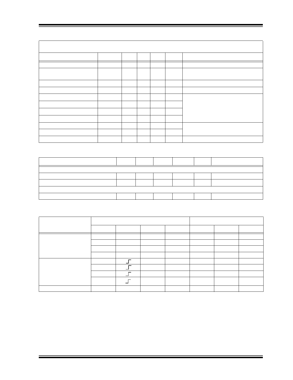
LOGIC CONTROL TABLE
MODE
LOGIC INPUTS
TX
N
, OUTPUT
OEN
CLK
PIN
X
NINX
VPP
VNN
RGND
Asynchronous Mode
Output Change on
PIN/NIN
1
VLL
0
0
OFF
OFF
ON
1
VLL
1
0
ON
OFF
OFF
1
VLL
0
1
OFF
ON
OFF
1
VLL
1
1
OFF
OFF
OFF
Synchronous Mode
Output Change at Retim-
ing Clock (CLK) Rising
Edge, registered by
PIN/NIN
1
0
0
OFF
OFF
ON
1
1
0
ON
OFF
OFF
1
0
1
OFF
ON
OFF
1
1
1
OFF
OFF
OFF
Disabled
0
X
X
X
OFF
OFF
OFF
AC ELECTRICAL CHARACTERISTICS (CONTINUED)
Electrical Specifications: V
LL
= +3.3V, V
DD
= +3.3V, V
PP
= +60V, V
NN
= –60V, V
CLK
= +3.3V, T
A
= 25°C unless
otherwise indicated.
Parameter
Sym.
Min.
Typ.
Max.
Unit
Conditions
HV7350
DS20005627A-page 6
2016 Microchip Technology Inc.
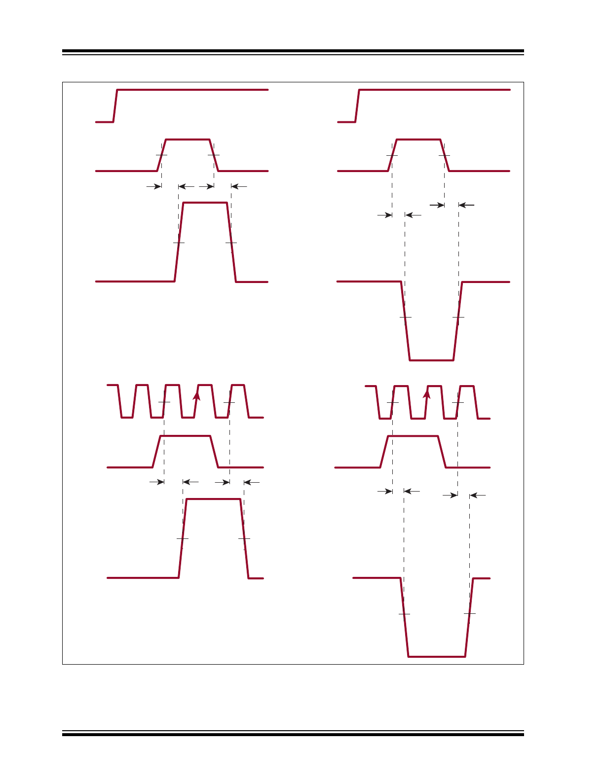
Timing Waveforms
CLK
PINn
(NINn = 0)
NINn
(PINn = 0)
NINn
(PINn = 0)
CLK
CLK
CLK
I
TXn
I
TXn
0
I
TXn
0
50%
50%
50%
50%
t
d1
t
d4
t
d2
t
d3
I
OUT
I
OUT
I
OUT
I
OUT
t
dc
t
dc
t
dc
t
dc
50%
50%
0
0
I
TXn
Synchronous Mode
Asynchronous Mode
PINn
(NINn = 0)
2016 Microchip Technology Inc.
DS20005627A-page 7
HV7350
2.0
PAD DESCRIPTION
Table 2-1
details the description of pads in HV7350.
Refer to
Package Type
for the location of pins.
TABLE 2-1:
PAD FUNCTION TABLE
Pin
Number
Pin
Name
Description
1
PIN2
Input logic control of high-voltage output P-FET for Channel 2; High = on; Low = off
(See
Logic Control Table
.)
2
NIN2
Input logic control of high-voltage output N-FET for Channel 2; High = on; Low = off
(See
Logic Control Table
.)
3
PIN3
Input logic control of high-voltage output P-FET for Channel 3; High = on; Low = off
(See
Logic Control Table
.)
4
NIN3
Input logic control of high-voltage output N-FET for Channel 3; High = on; Low = off
(See
Logic Control Table
.)
5
PIN4
Input logic control of high-voltage output P-FET for Channel 4; High = on; Low = off
(See
Logic Control Table
.)
6
NIN4
Input logic control of high-voltage output N-FET for Channel 4; High = on; Low = off
(See
Logic Control Table
.)
7
OEN
Output enable; High = on; Low = off (See
Logic Control Table
.)
8
REN
Built-in positive and negative 5V voltage regulators enable; High = on; Low = off
If REN = 0, four isolated 5V power supplies may provide, as external supplies, for the VPP to CPF, CNF to
VNN, CPOS to GND and GND to CNEG pins. Note that between VPP to CPF and CNF to VNN, two must be
floating supplies. (See
Logic Control Table
.)
9
PIN5
Input logic control of high-voltage output P-FET for Channel 5; High = on; Low = off
(See
Logic Control Table
.)
10
NIN5
Input logic control of high-voltage output N-FET for Channel 5; High = on; Low = off
(See
Logic Control Table
.)
11
PIN6
Input logic control of high-voltage output P-FET for Channel 6; High = on; Low = off
(See
Logic Control Table
.)
12
NIN6
Input logic control of high-voltage output N-FET for Channel 6; High = on; Low = off
(See
Logic Control Table
.)
13
PIN7
Input logic control of high-voltage output P-FET for Channel 7; High = on; Low = off
(See
Logic Control Table
.)
14
NIN7
Input logic control of high-voltage output N-FET for Channel 7; High = on; Low = off
(See
Logic Control Table
.)
15
PIN8
Input logic control of high-voltage output P-FET for Channel 8; High = on; Low = off
(See
Logic Control Table
.)
16
NIN8
Input logic control of high-voltage output N-FET for Channel 8; High = on; Low = off
(See
Logic Control Table
.)
17
VLL
Logic supply voltage and reference input (+3.3V)
18
GND
Logic and circuit return ground (0V)
19
VDD
Positive voltage power supply (+3.3V)
20
VPP
Positive high-voltage power supply (+10V to +60V)
21
VPP
22
VPP
23
CPF
Built-in linear voltage VPF regulator output decoupling capacitor pin, 1 uF from VPP to CPF for every CPF pin
24
CNF
Built-in linear voltage VNF regulator output decoupling capacitor pin, 1 uF from CNF to VNN for every CNF
pin
25
VNN
Negative high-voltage power supply (–10V to –60V)
26
VNN
27
VNN
28
TX8
T
X
pulser Channel 8 output
29
RGND
Damping ground and bleed resistors common return ground
HV7350
DS20005627A-page 8
2016 Microchip Technology Inc.
30
TX7
T
X
pulser Channel 7 output
31
RGND
Damping ground and bleed resistors common return ground
32
TX6
T
X
pulser Channel 6 output
33
RGND
Damping ground and bleed resistors common return ground
34
TX5
T
X
pulser Channel 5 output
35
CNEG
Built-in linear voltage –5V regulator output decoupling capacitor pin, 1 uF from CNEG to GND
36
CPOS
Built-in linear voltage +5V regulator output decoupling capacitor pin, 1 uF from CPOS to GND
37
TX4
T
X
pulser Channel 4 output
38
RGND
Damping ground and bleed resistors common return ground
39
TX3
T
X
pulser Channel 3 output
40
RGND
Damping ground and bleed resistors common return ground
41
TX2
T
X
pulser Channel 2 output
42
RGND
Damping ground and bleed resistors common return ground
43
TX1
T
X
pulser Channel 1 output
44
VNN
Negative high-voltage power supply (–10V to –60V)
45
VNN
46
VNN
47
CNF
Built-in linear voltage VNF regulator output decoupling capacitor pin, 1 uF from CNF to VNN for every CNF
pin
48
CPF
Built-in linear voltage VPF regulator output decoupling capacitor pin, 1 uF from VPP to CPF for every CPF pin
49
VPP
Positive high-voltage power supply (+10V to +60V)
50
VPP
51
VPP
52
VDD
Positive voltage power supply (+3.3V)
53
GND
Logic and circuit return ground (0V)
54
CLK
Retiming register clock input. Connect to VLL to disable the retiming function.
55
PIN1
Input logic control of high-voltage output P-FET for Channel 1; High = on; Low = off
(See
Logic Control Table
.)
56
NIN1
Input logic control of high-voltage output N-FET for Channel 1; High = on; Low = off
(See
Logic Control Table
.)
VSUB
(Thermal Pad)
Substrate bottom is internally connected to the central thermal pad on the bottom of package. It must be con-
nected to GND (0V) externally.
TABLE 2-1:
PAD FUNCTION TABLE (CONTINUED)
Pin
Number
Pin
Name
Description
2016 Microchip Technology Inc.
DS20005627A-page 9
HV7350
3.0
FUNCTIONAL DESCRIPTION
Follow the steps below to power up and power down
the HV7350:
POWER-UP AND POWER-DOWN SEQUENCE (
Note 1
)
Power-Up
Power-Down
Step
Description
Step
Description
1
V
LL
with logic signal low
1
All logic signals go to low
2
V
DD
2
V
PP
and V
NN
3
REN = 1 (external supplies on)
3
REN = 0 (external supplies off)
4
V
PP
and V
NN
4
V
DD
5
Logic control signals active
5
V
LL
Note 1: Powering up or down in any arbitrary sequence will not damage the device. The power-up sequence and
power-down sequence are only recommended to minimize possible inrush current.
OUTPUT CURRENT AND R
ON
(
Note 1
,
Note 4
)
I
SC
2
R
onP
R
onN
I
DMP
3
R
onDP
R
onDN
1.5A
13Ω
6.5Ω
1.5A
13Ω
8Ω
Note 1: V
PP
/V
NN
= +/-60V; V
DD
= +3.3V; REN
= 1
2: I
SC
is current into 1Ω to GND.
3: I
DMP
is current from +/–30V connected to T
X
pin.
4: Maximum pulse width for current measurement on T
X
pin is 20 ns.
HV7350
DS20005627A-page 10
2016 Microchip Technology Inc.
4.0
PACKAGING INFORMATION
4.1
Package Marking Information
Legend: XX...X
Product Code or Customer-specific information
Y
Year code (last digit of calendar year)
YY
Year code (last 2 digits of calendar year)
WW
Week code (week of January 1 is week ‘01’)
NNN
Alphanumeric traceability code
Pb-free JEDEC
®
designator for Matte Tin (Sn)
*
This package is Pb-free. The Pb-free JEDEC designator ( )
can be found on the outer packaging for this package.
Note:
In the event the full Microchip part number cannot be marked on one line, it will
be carried over to the next line, thus limiting the number of available
characters for product code or customer-specific information. Package may or
not include the corporate logo.
3
e
3
e
56-lead QFN
Example
YYWWNNN
YYWWNNN
e3
XXXXXX
XXXXXX
HV7350K6
HV7350K6
e3
1621987
1621987