

2017 Microchip Technology Inc.
DS20005920A-page 1
HV7322
Features
• High-Voltage CMOS Technology for High
Performance
• 8-Channel, True 5-Level or Pseudo 7-Level,
±80V, 2A, with Return-to-Zero (RTZ) to True Zero
Voltage
• Programmable ±0.5A, 1.0A, 1.5A and 2A Output
Current from V
PP1
/V
NN1
• Integrated Radio Frequency (RF) Blocking,
Clamp Diode and RX Damp
• 13
Transmit/Receive (T/R) and Low Voltage
(LV) Switches Allow Receiver Multiplexing
• 160
Auto-Bleeding Switches for RTZ True Zero
• 220 MHz Clock Retiming Synchronization
Capability
• 2.5V, 3.3V Logic Control Voltage, designed to
work with FPGA Inputs and Outputs (I/O) directly.
• Adjusting T/R Switch Delay, Avoid Echo
Saturating
• TX Output Frequency up to 20 MHz
• -40 dB HD2 Second Harmonic Distortion at
5 MHz
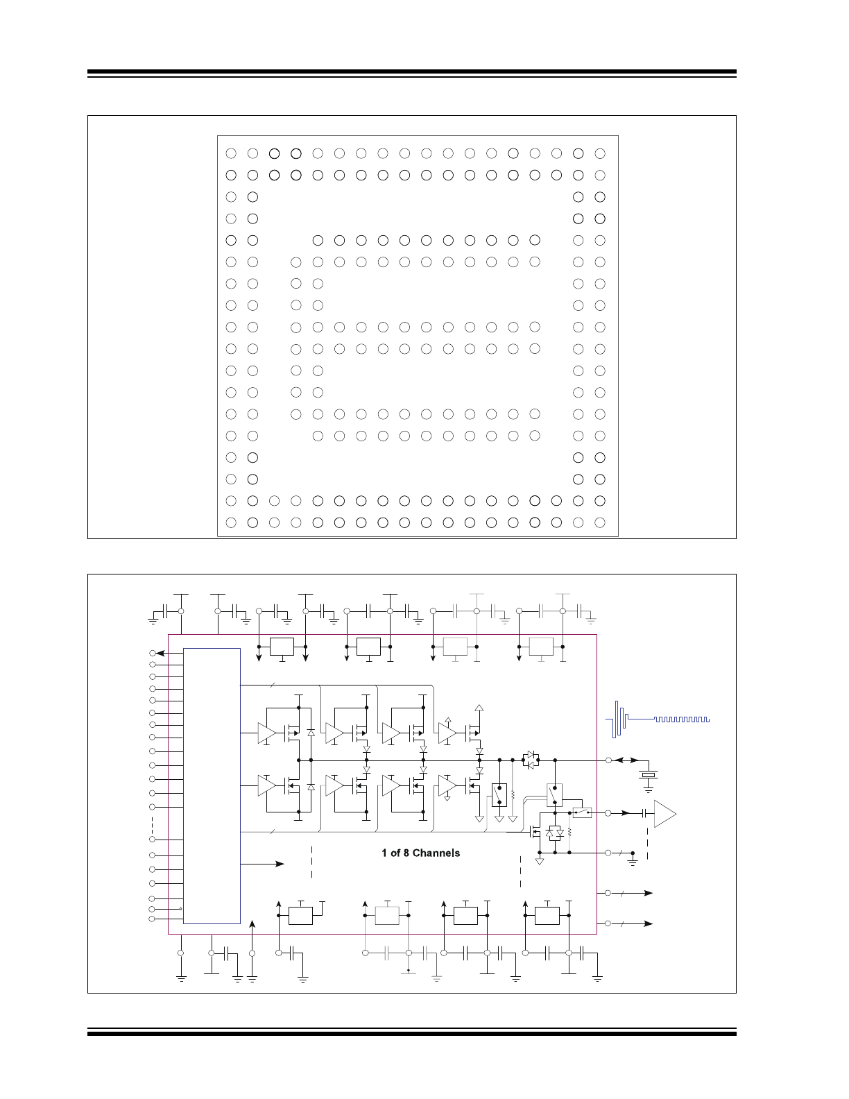
• 12 mm x 12 mm x 1.20 mm 206-Lead TFBGA
Package
Applications
• Medical ultrasound imaging system
• NDT (nondestructive testing) ultrasound
transmission pulsers
• Piezoelectric or capacitive transducer drivers
Description
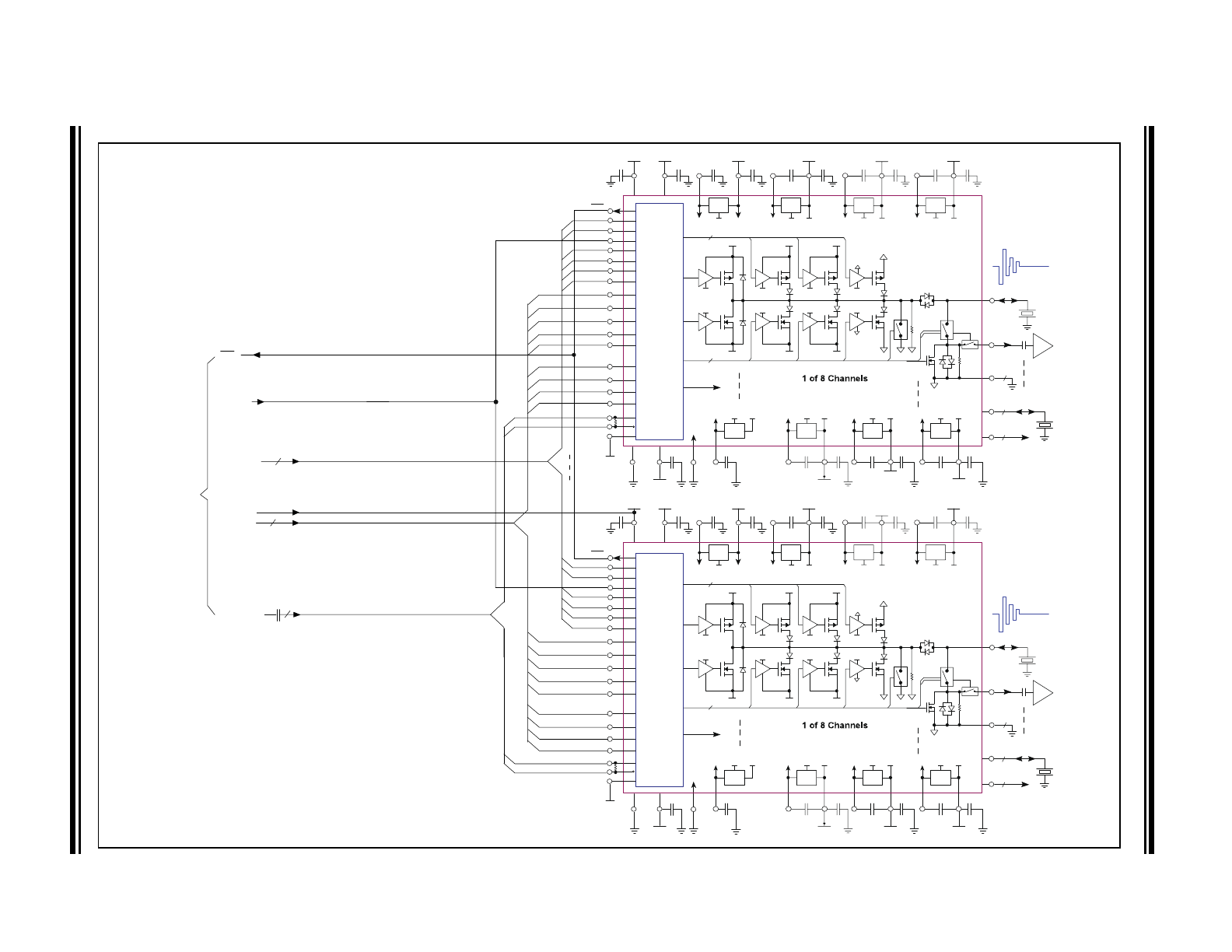
The HV7322 device is an 8-channel, true 5-level or
pseudo 7-level, high-voltage pulser, with integrated T/R
switches. HV7322 is designed for medical ultrasound
applications. It is also fitted for NDT and other
transducer drive applications.
The HV7322 device’s output has seven different volt-
age levels: V
PP0,1,2
, V
NN0,1,2
and GND. The output
MOSFET transistors can provide up to ±2A of current
at the maximum voltage of ±80V. HV7322 has channel
RTZ for the return-to-zero feature. The three sets of
high-voltage outputs, with ±2A of peak output current in
B-Mode and programmable 2-bit, use the V
PP1
/V
NN1
voltage rails for the CW-Mode (IM<1:0> = 0), in order to
reduce the CW-Mode power dissipations on chip.
The high-voltage T/R and LV analog switches (total
13
) and RX damp switch are Integrated in each chan-
nel, while the 160
RTZ switches dedicated for true
zero voltage minimize the received noise.
The 220 MHz differential retiming clock inputs and
built-in registers are capable of providing low jitter in
Continuous Wave Doppler (CWD) mode, in Pulse
Wave (PW) mode or in B-mode. The clock synchroni-
zation realigns the logic input signals to a master clock,
which reduces various propagation delays caused by
FPGA inaccuracies and/or long PCB traces.
The integrated circuit (IC) has built-in gate-driver float-
ing voltage regulators, allowing V
PP0,1,2
and V
NN0,1,2
high-voltage rails to move the voltage interdependently
from 0 to ±80V or to 60V. Each of the pulsers has output
voltage overshoot clamping diodes to the highest level
of the supply pin of V
PP0
or V
NN0
rails respectively. The
differential clock inputs take Differential Clock or
LVCMOS output signals. The logic control voltages are
designed to work with the Differential Clock or the
LVCMOS logic families directly.
8-Channel 7-Level ±80V High-Voltage Pulser with T/R Switches
HV7322
DS20005920A-page 2
2017 Microchip Technology Inc.
Package Types
HV7322 - Block Diagram
V
DD
OEN
IM0
CLKP
REN
CWEN
CLKN
IM1
TLV0 TLV1
C
NF1
V
NN2
V
NN0
C
PF2
C
NF0
VPP2
C
PF1
V
PP1
C
PF0
POS4
NEG4
SLA4
SLB4
POS5
NEG5
SLA5
SLB5
POS6
NEG6
SLA6
SLB6
POS7 NEG7
SLB7
SLA7
V
GN
POS0 NEG0 SLA0 SLB0
POS1
NEG1
SLA1
SLB1
POS2
NEG2
SLA2
SLB2
POS3
NEG3
SLA3
SLB3
GND
VLL
TX4
RX4
TX5
RX5
TX6
RX6
TX7
RX7
TX0
RX0
TX1
RX1
TX2
RX2
TX3
RX3
C
POS
C
NEG
R
GND
V
DD
GND
V
GP
C
POS
DCLKEN
OTP
N
NC
NC
NC
NC
R
GND
R
GND
R
GND
R
GND
R
GND
R
GND
R
GND
R
GND
R
GND
V
SUB
V
SUB
R
GND
R
GND
R
GND
R
GND
R
GND
R
GND
R
GND
CNF1
VNN1
VPP0 CPF0
CNEG
RGND
V
NN0
C
NF0
C
PF1
V
PP1
C
NEG
V
NN2
C
PF2
C
NF2
C
POS
C
NEG
C
NEG
C
NEG
CNF1
VNN1
V
NN2
V
NN0
C
PF2
C
PF0
CPF2
V
PP2
VPP0
C
NF1
V
PP1
CPF0
C
POS
RGND
CNF1
V
NN1
CPF0
CNEG
V
NN0
C
PF0
C
PF1
V
PP1
V
NN2
CPF2
C
NF2
V
PP2
GND
GND
GND
GND
V
PP0
V
NN1
V
PP2
GND
GND
V
PP0
GND
GND
GND
GND
NC
GND
GND
GND
GND
GND
GND
GND
C
NF1
V
NN2
V
NN0
C
PF2
C
NF0
CPF2
C
PF1
V
PP1
C
PF0
VPP0 CPF0
V
NN0
C
PF0
C
PF1
V
PP1
V
NN2
C
PF2
C
NF2
V
NN1
V
NN2
V
NN0
C
PF2
C
NF0
C
NF1
V
NN1
V
NN0
C
PF0
C
PF1
V
PP1
V
NN2
C
NF2
V
PP0
V
NN1
V
PP2
V
PP0
VPP2
V
PP2
V
PP1
V
PP2
V
NN2
V
NN1
V
PP1
V
PP0
V
PP0
V
PP0
V
NN0
R
GND
C
NEG
V
NN1
V
NN1
V
PP2
V
PP2
V
NN2
V
PP2
V
PP2
V
NN1
V
NN1
V
PP1
V
PP0
V
PP0
V
PP0
V
NN0
MODE
1
2
3
4
5
6
7
8
9
10
11
12
13
14
15
16
17
18
A
B
C
D
E
F
G
H
J
K
L
M
N
P
R
T
U
V
MODE
REN
IM0
IM1
273
POS0
NEG0
SLA0
POS7
NEG7
SLA7
CLKP
+2.5V/3.3
+5V
+10V
-10V
GND
V
GN
V
SUB
C
NEG
V
LL
V
DD
C
POS
V
GP
0.47µF
2µF
2µF
2µF
2µF
2µF
V
NEG
GND
V
GN
SUB
GND
to
Ch 1-7
Tx0
Rx0
Tx1~7
Rx1~7
+2V to +80V
C
PF0
V
PP0
2µF
1µF 100V
+2V to +60V
C
PF1
V
PP1
2µF
1µF 100V
-2V to -80V
C
FN0
V
NN0
1µF 100V
2µF
V
NF0
V
GP
V
NN0
-2V to -60V
C
NF1
V
NN1
2µF
V
NF1
V
GP
V
NN1
1µF 100V
Logic
and
Reti ming
RxDMP0
TRSW0
RTZSW0
R
b
+60V to -60V
C
PF2
V
PP2
2µF
1µF 100V
-60V to +60V
C
FN2
V
NN2
2µF
V
NF2
V
GP
V
NN2
1µF 100V
SLB0
SLB7
CLKN
R
b
LVSW0
OEN
LR
LR
LR
LR
LR
V
NEG
LR
V
NF0
LR
V
NF1
LR
V
NF2
TLV0
TLV1
DCLKEN
CWEN
X0
Rx0
V
POS
V
PF0
V
PP0
V
PF1
V
PP1
V
PF2
V
GN
V
PP2
V
POS
V
PF0
V
PF1
V
PF2
V
GP
V
NN0
V
NF0
V
PF0
V
NN2
V
NF2
V
PF2
V
POS
V
NEG
V
NN1
V
NF1
V
PF1
V
GN
V
GN
V
PP0
V
PP2
V
PP1
R
GND
R
GND
V
N
1
2
2017
Microchip Technology Inc.
D
S
20005920A-
page
3
HV7322
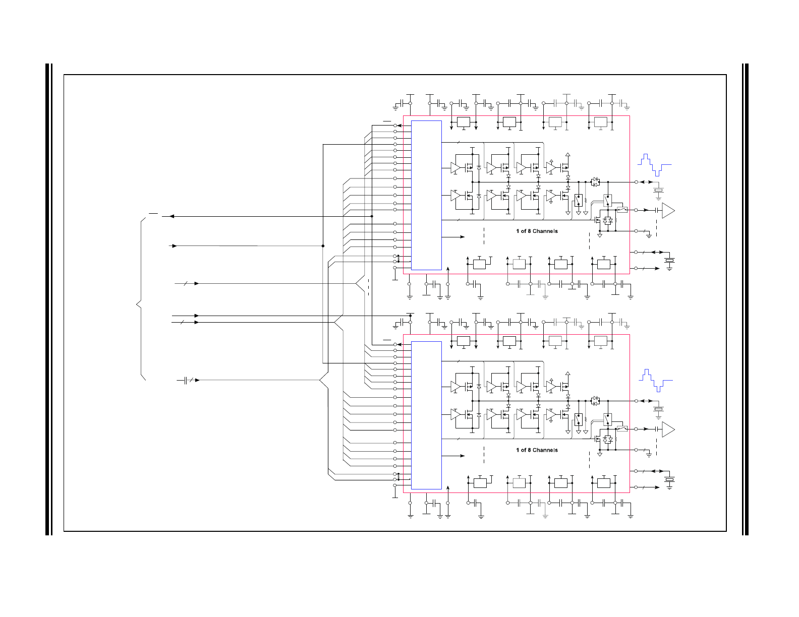
HV7322 - Typical 7-Level Application Diagram
Tx FPGA I/Os
OTP
CTRL[5:0]
DT[127:0]
MODE
REN
IM0
IM1
OTP
POS0
NEG0
SLA0
POS7
NEG7
SLA7
CLKP
GND
+2.5V
+5V
+10V
-10V
0.47µF
2µF
2µF
2µF
2µF
2µF
GND
SUB
to
Ch 1-7
X0
+80V
-80V
-40V
+40V
-20V
+20V
0V
Rx0
Tx0
Rx0
Tx1~7
Rx1~7
+80V
2µF
1µF 100V
+40V
2µF
1µF 100V
-80V
1µF 100V
2µF
-40V
2µF
1µF 100V
Logic
and
Reti ming
RxDMP0
TRSW0
RTZSW0
R
b
2µF
1µF 100V
2µF
1µF 100V
SLB0
SLB7
CLKN
R
b
LVSW0
OEN
LR
LR
LR
LR
LR
LR
LR
LR
TLV0
TLV1
MODE
REN
IM0
IM1
OTP
POS0
NEG0
SLA0
POS7
NEG7
SLA7
CLKP
+2.5V
+5V
+10V
-10V
GND
0.47µF
2µF
2µF
2µF
2µF
2µF
GND
SUB
GND
to
Ch 1-7
X23
Rx0
Tx0
Rx0
Tx1~7
Rx1~7
+80V
2µF
1µF 100V
+40V
2µF
1µF 100V
-80V
1µF 100V
2µF
-40V
2µF
1µF 100V
Logic
and
Reti ming
RxDMP0
TRSW0
RTZSW0
R
b
2µF
1µF 100V
2µF
1µF 100V
SLB0
SLB7
CLKN
R
b
LVSW0
OEN
LR
LR
LR
LR
LR
LR
LR
LR
TLV0
TLV1
CLKP/CLKN
VCC_2V5
TRUE5L
(Ture 5-Level or
7-Level Control)
X1 to 7
X24 to 31
U4
U1
DCLKEN
+2.5V
+2.5V
100
100
0.1µFx2
2
-20V
-20V
+20V
+20V
+80V
-80V
-40V
+40V
-20V
+20V
0V
CWEN
CWEN
V
LL
V
DD
C
POS
V
GP
C
PF0
V
PP0
C
PF1
V
PP1
C
PF2
V
PP2
V
LL
V
DD
C
POS
V
GP
C
PF0
V
PP0
C
PF1
V
PP1
C
PF2
V
PP2
V
POS
V
PP0
V
PP2
V
PF0
V
PP0
V
PF1
V
PP1
V
PP1
V
PF2
V
GN
V
PP2
V
POS
V
PF0
V
PF1
V
PF2
V
GP
R
GND
V
NN0
V
NF0
V
PF0
V
NN2
V
NF2
V
PF2
R
GND
V
POS
V
NEG
V
NN1
V
NF1
V
PF1
V
GN
V
SUB
C
NEG
V
NEG
V
GN
C
NF0
V
NN0
V
1)0
V
GP
V
NN0
C
NF1
V
NN1
V
NF1
V
GP
V
NN1
C
NF2
V
NN2
V
NF2
V
GP
V
NN2
V
NEG
V
NF0
V
NF1
V
NF2
R
GND
R
GND
V
GN
V
SUB
C
NEG
V
NEG
V
GN
C
NF0
V
NN0
V
1)0
V
GP
V
NN0
C
NF1
V
NN1
V
NF1
V
GP
V
NN1
C
NF2
V
NN2
V
NF2
V
GP
V
NN2
V
NEG
V
NF0
V
NF1
V
NF2
V
POS
V
PP0
V
PP2
V
PF0
V
PP0
V
PF1
V
PP1
V
PP1
V
PF2
V
GN
V
PP2
V
POS
V
PF0
V
PF1
V
PF2
V
GP
V
NN0
V
NF0
V
PF0
V
NN2
V
NF2
V
PF2
V
POS
V
NEG
V
NN1
V
NF1
V
PF1
DCLKEN
GND
V
GN
V
GN
V
GN
V
GN
N
HV7322
DS200059
20A-page 4
2017 Microchip T
echnolo
gy Inc.
HV7322 - Typical True 5-Level Application Diagram
Tx FPGA I/Os
OTP
CTRL[5:0]
DT[127:0]
MODE
REN
IM0
IM1
OTP
POS0
NEG0
SLA0
POS7
NEG7
SLA7
CLKP
GND
+2.5V
+5V
+10V
-10V
V
GN
V
SUB
C
NEG
V
LL
V
DD
C
POS
V
GP
0.47µF
2µF
2µF
2µF
2µF
2µF
V
NEG
GND
V
GN
SUB
GND
V
POS
to
Ch 1-7
X0
Rx0
Tx0
Rx0
R
GND
Tx1~7
Rx1~7
V
NN0
V
NF0
V
PF0
V
PP0
V
NN2
V
NF2
V
PF2
V
PP2
+80V
C
PF0
V
PP0
2µF
1µF 100V
V
PF0
V
GN
V
PP0
+40V
C
PF1
V
PP1
2µF
1µF 100V
V
PF1
V
GN
V
PP1
-80V
C
NF0
V
NN0
1µF 100V
2µF
V
1)0
V
GP
V
NN0
-40V
C
NF1
V
NN1
2µF
V
NF1
V
GP
V
NN1
1µF 100V
Logic
and
Reti ming
R
GND
RxDMP0
TRSW0
RTZSW0
V
POS
V
NEG
R
b
V
NN1
V
NF1
V
PF1
V
PP1
C
PF2
V
PP2
2µF
1µF 100V
V
PF2
V
GN
V
PP2
C
NF2
V
NN2
2µF
V
NF2
V
GP
V
NN2
1µF 100V
SLB0
SLB7
CLKN
R
b
LVSW0
OEN
LR
V
POS
LR
V
PF0
LR
V
PF1
LR
V
PF2
LR
V
NEG
LR
V
NF0
LR
V
NF1
LR
V
NF2
TLV0
TLV1
MODE
REN
IM0
IM1
OTP
POS0
NEG0
SLA0
POS7
NEG7
SLA7
CLKP
+2.5V
+5V
+10V
-10V
GND
0.47µF
2µF
2µF
2µF
2µF
2µF
GND
SUB
GND
to
Ch 1-7
X23
Rx0
Tx0
Rx0
Tx1~7
Rx1~7
+80V
2µF
1µF 100V
+40V
2µF
1µF 100V
-80V
1µF 100V
2µF
-40V
2µF
1µF 100V
Logic
and
Reti ming
RxDMP0
TRSW0
RTZSW0
R
b
2µF
1µF 100V
2µF
1µF 100V
SLB0
SLB7
CLKN
R
b
LVSW0
OEN
LR
LR
LR
LR
LR
LR
LR
LR
TLV0
TLV1
CLKP/CLKN
VCC_2V5
TRUE5L
(Ture 5-Level or
7-Level Control)
0V
+80V
-80V
-40V
+40V
X1 to 7
X24 to 31
U4
U1
+2.5V
+2.5V
100
100
0.1µFx2
2
+40V
+40V
-40V
0V
+80V
-80V
-40V
+40V
-40V
CWEN
CWEN
V
GP
V
LL
V
DD
C
POS
V
GP
C
PF0
V
PP0
C
PF1
V
PP1
C
PF2
V
PP2
V
POS
V
PF0
V
GN
V
PP0
V
PF1
V
GN
V
PP1
V
PF2
V
GN
V
PP2
V
POS
V
PF0
V
PF1
V
PF2
V
GP
V
PP0
V
PP2
V
PP1
V
NF0
V
PF0
V
NF2
V
PF2
V
POS
V
NEG
V
NF1
V
PF1
V
NN0
V
NN2
V
NN1
V
NEG
V
GN
R
GND
V
FN0
V
GP
V
NN0
V
NF1
V
GP
V
NN1
R
GND
V
NF2
V
GP
V
NN2
V
NEG
V
NF0
V
NF1
V
NF2
V
GN
V
SUB
C
NEG
C
NF0
V
NN0
C
NF1
V
NN1
C
NF2
V
NN2
DCLKEN
DCLKEN
2017 Microchip Technology Inc.
DS20005920A-page 5
HV7322
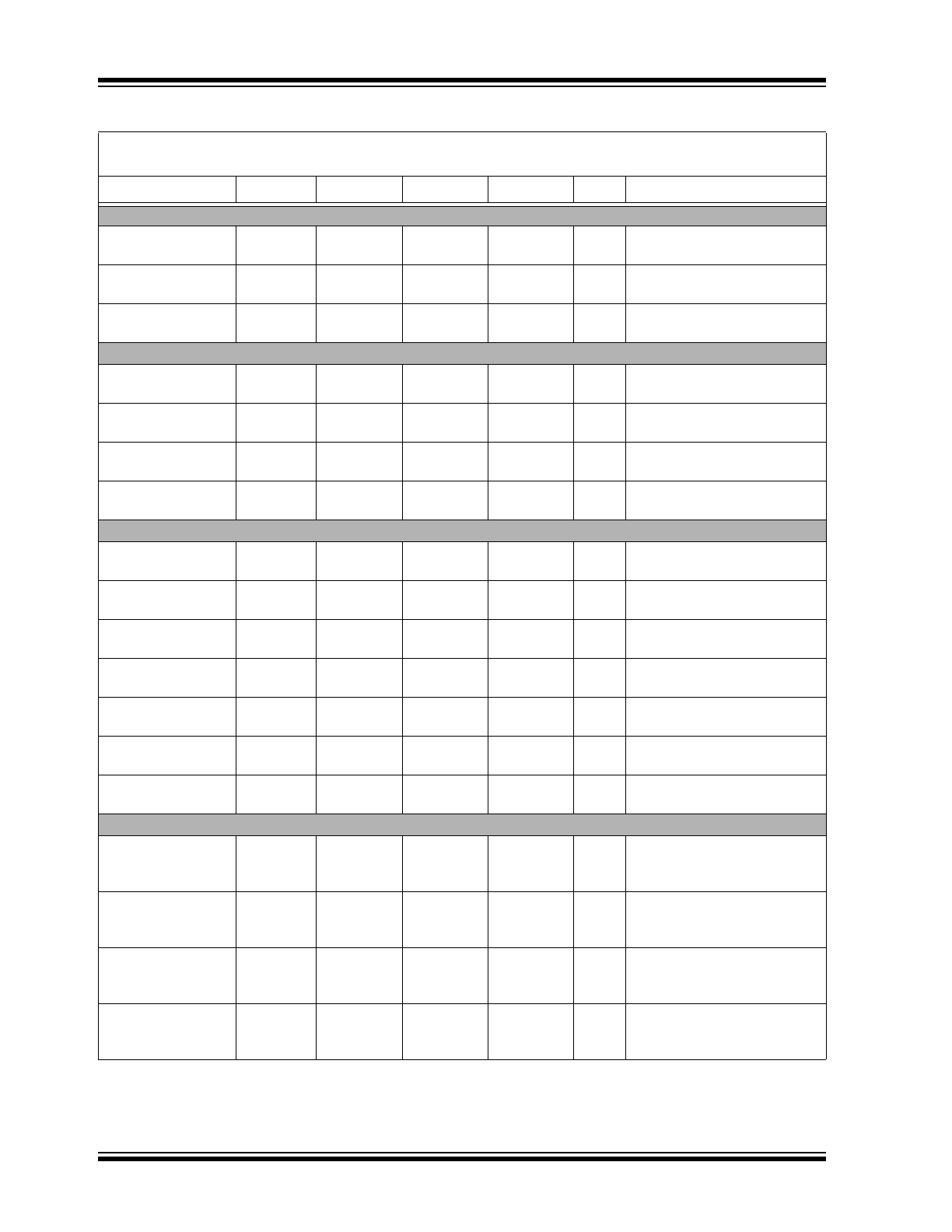
1.0
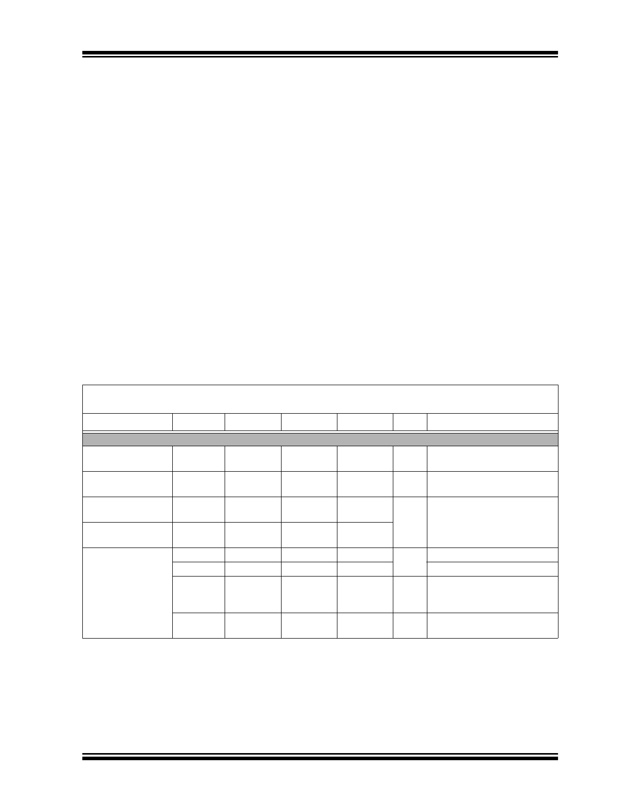
ELECTRICAL CHARACTERISTICS
Absolute Maximum Ratings†
Logic Voltage (V
LL
).................................................................................................................................... –0.5V to +5.5V
All I/O and CLK pin voltage (V
IO
) .............................................................................................................. –0.5V to +5.5V
Positive voltage supply (V
DD
).................................................................................................................... –0.5V to +5.5V
Positive gate driver supply (V
GP
) ............................................................................................................ –0.5V to +13.5V
Negative gate driver supply (V
GN
) .......................................................................................................... –13.5V to +0.5V
High-voltage positive supply (V
PP0
) ........................................................................................................... –1.0V to +85V
High-voltage positive supply (V
PP1
) ........................................................................................................... –1.0V to +65V
High-voltage positive supply (V
PP2
) ............................................................................................................ –65V to +65V
High-voltage negative supply (V
NN0
) ......................................................................................................... –85V to +1.0V
High-voltage negative supply (V
NN1
) ......................................................................................................... –65V to +1.0V
High-voltage negative supply (V
NN2
) .......................................................................................................... –65V to +65V
TX pin voltage (V
TX
).................................................................................................................................... –85V to +85V
RX pin to GND voltage (V
RX
) .......................................................................................................................±0.7 to ±1.4V
Maximum not-latch-up current (I
LU
) ................................................................................................................... +100 mA
ESD HBM Rating T
X
, V
PP
, V
NN
, CPF, CNF, CNEG, CPOS, V
GP
, V
GN
, R
X
, R
GND
pins ......................... –0.50 to +0.50 kV
ESD HBM Rating – all other LV pins......................................................................................................... –2.0 to +2.0 kV
† Notice: Stresses above those listed under “Maximum Ratings” may cause permanent damage to the device. This is a
stress rating only and functional operation of the device at those or any other conditions above those indicated in the
operational sections of this specification is not intended. Exposure to maximum rating conditions for extended periods
may affect device reliability.
ELECTRICAL CHARACTERISTICS
Electrical specifications: V
LL
= +2.5V, V
DD
= +5.0V, V
PP0
= +80V, V
NN0
= -80V, V
PP1,2
= +60V, V
NN1,2
= –60V,
V
GP
= +10V, V
GN
= -10V, V
SUB
= 0V, MODE = 0, OEN = REN = 1, T
A
= 25°C.
Parameter
Sym.
Min.
Typ.
Max.
Unit
Conditions
Operating Supply Voltages
Positive Logic
Supply
V
LL
2.25
2.50
3.60
V
—
Internal Voltage
Supply
V
DD
4.75
5.0
5.25
V
—
Positive Gate
Driver Supply
V
GP
8.0
10
12
V
—
Negative Gate
Driver Supply
V
GN
–12
–10
–8.0
High Voltage
Positive Supply
V
PP0
0
—
80
V
Must be V
PP0
≥ V
PP1
and V
PP2
V
PP1
0
—
60
Must be V
PP1
V
PP0
V
PP2
0
—
60
V
MODE = 0
In the 7-Level Mode.
Must be V
PP2
V
PP0
V
PP2
V
NN1
- 0.7
V
NN1
V
NN1
+ 0.7
V
MODE = 1
|V
PP2
- V
NN1
|
0.7
Note 1: Characterized only; not 100% tested in production.
2: Design guidance only.
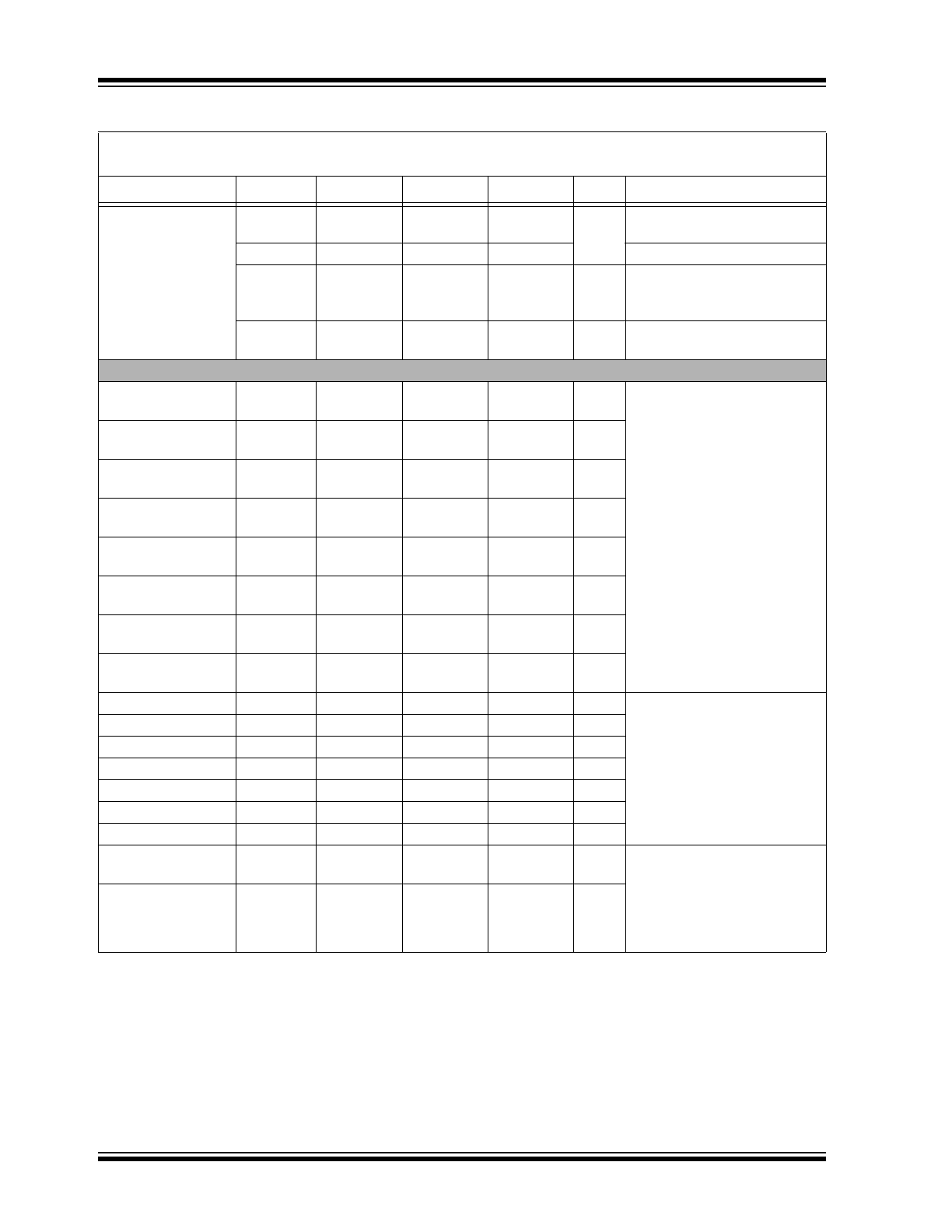
HV7322
DS20005920A-page 6
2017 Microchip Technology Inc.
High Voltage
Negative Supply
V
NN0
–80
—
0
V
Must be V
NN0
V
NN1
and
V
NN2
V
NN1
–60
—
0
Must be V
NN1
≥ V
NN0
V
NN2
–60
—
0
V
MODE = 0
In the 7-Level Mode.
Must V
NN2
≥ V
NN0
V
NN2
V
PP1
- 0.7
V
PP1
V
PP1
+ 0.7
V
MODE = 1
|V
NN2
- V
PP1
|
0.7
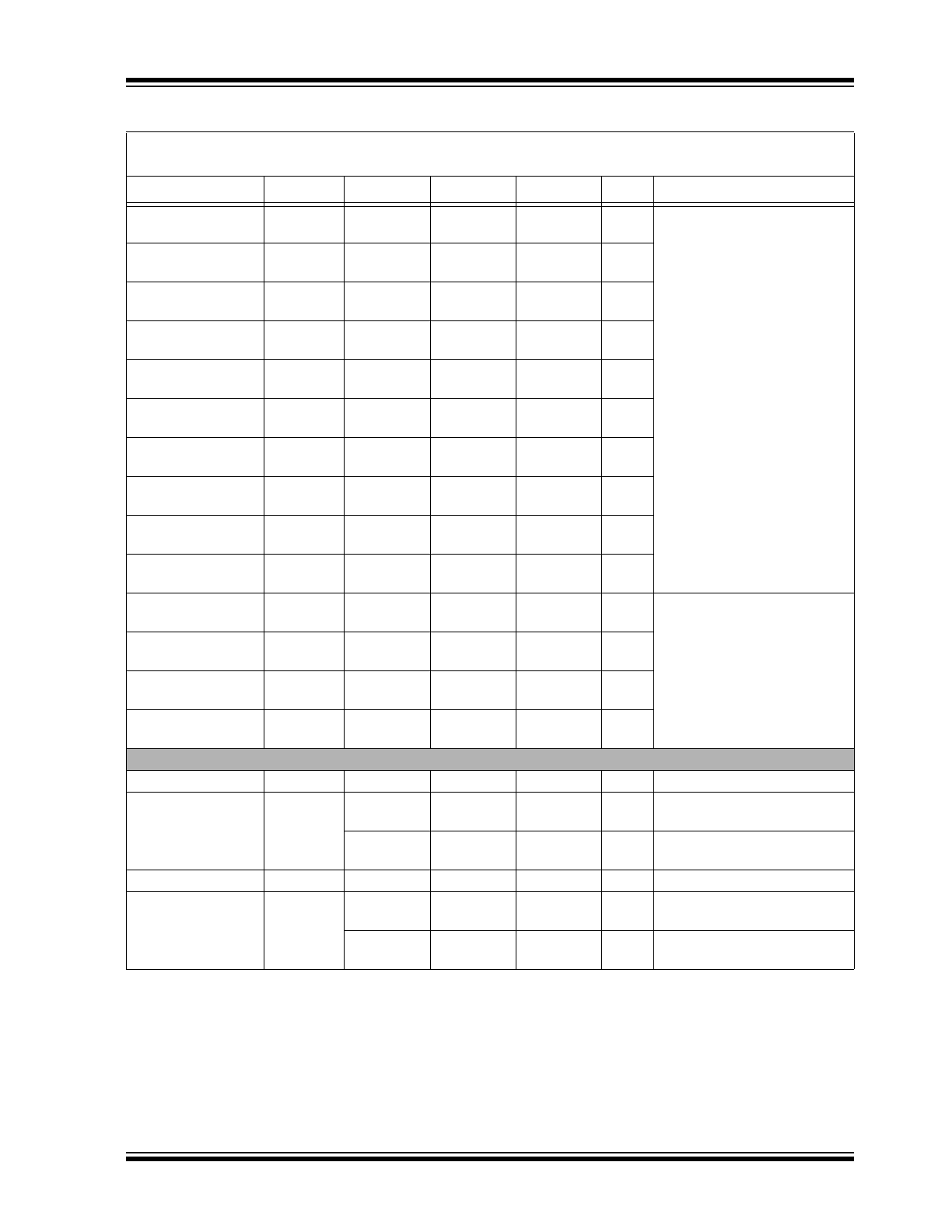
Operating Supply Current
V
LL
Quiescent
Current
I
LLQ
—
2
5
μA
OEN = REN = 0
V
DD
Quiescent
Current
I
DDQ
—
54
65
µA
V
PP0
Quiescent
Current
I
PP0Q
—
—
15
µA
V
NN0
Quiescent
Current
I
NN0Q
–15
—
—
µA
V
PP1
Quiescent
Current
I
PP1Q
—
—
20
µA
V
NN1
Quiescent
Current
I
NN1Q
–20
—
—
µA
V
PP2
Quiescent
Current
I
PP2Q
—
—
40
µA
V
NN2
Quiescent
Current
I
NN2Q
–40
—
—
µA
V
DD
Current
I
DDEN
—
1
2
mA
DCLKEN = 0
f
TX
= 0 MHz
f
CLK
= 0
V
PP0
Current
I
PP0EN
—
0.26
0.4
mA
V
NN0
Current
I
NN0EN
–0.4
–0.34
—
mA
V
PP1
Current
I
PP1EN
—
0.12
0.3
mA
V
NN1
Current
I
NN1EN
–0.3
–0.13
—
mA
V
PP2
Current
I
PP2EN
—
0.12
0.3
mA
V
NN2
Current
I
NN2EN
–0.3
–0.12
—
mA
V
LL
Current with
Re-Timing
I
LL_DCLK
—
0.41
0.45
mA
DCLKEN = 1, f
CLK
= 160 MHz
TX one-channel output active,
no load.
The continuous values are cal-
culated from measured
burst-mode 5 MHz cases.
V
DD
Current with
Re-Timing
I
DD_DCLK
—
25
30
mA
ELECTRICAL CHARACTERISTICS (CONTINUED)
Electrical specifications: V
LL
= +2.5V, V
DD
= +5.0V, V
PP0
= +80V, V
NN0
= -80V, V
PP1,2
= +60V, V
NN1,2
= –60V,
V
GP
= +10V, V
GN
= -10V, V
SUB
= 0V, MODE = 0, OEN = REN = 1, T
A
= 25°C.
Parameter
Sym.
Min.
Typ.
Max.
Unit
Conditions
Note 1: Characterized only; not 100% tested in production.
2: Design guidance only.
2017 Microchip Technology Inc.
DS20005920A-page 7
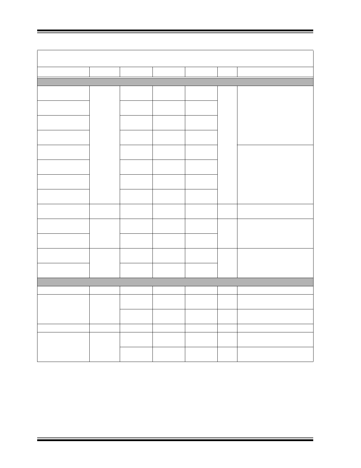
HV7322
V
LL
Maximum
Current in B-Mode
I
LL5
—
26
60
μA
DCLKEN = 0 f
CLK
= 0 MHz,
in B-Mode
TX one-channel output, no
loads.
The continuous values are
calculated from the measured
burst-mode 5 MHz cases.
I
NN25
and I
PP25
are only in
7-Level Mode.
V
DD
Maximum
Current in B-Mode
I
DD5
—
1.4
1.6
mA
V
GP
Maximum
Current in B-Mode
I
GP5
—
3.4
6
mA
V
GN
Maximum
Current in B-Mode
I
GN5
–16
–12.9
—
mA
V
PP0
Current
in B-Mode
I
PP05
—
102
115
mA
V
NN0
Current
in B-Mode
I
NN05
–105
–96
—
mA
V
PP1
Current
in B-Mode
I
PP15
—
85
95
mA
V
NN1
Current
in B-Mode
I
NN15
–95
–84
—
mA
V
PP2
Current
in B-Mode
I
PP25
—
94
105
mA
V
NN
Current
in B-Mode
I
NN25
–100
–91
—
mA
V
GP
Current
in CW-Mode
I
GPCW
—
1.5
2
mA
TX one-channel output 5 MHz,
continuous, no loads.
V
PP1
/V
NN1
= ±5V
in CW-Mode.
SLB = 0, SLA = 1,
Note 1
V
GN
Current
in CW-Mode
I
GNCW
–4.4
–4
—
mA
V
PP1
Current
in CW-Mode
I
PP1CW
—
24.4
26
mA
V
NN1
Current
in CW-Mode
I
NN1CW
-26
-23.5
—
mA
TX Output P-Channel MOSFET on V
PP0
, V
PP2
On-Resistance
R
ON_P0
—
13
16
I
SD
= 100 mA
Peak Output Current
I
OUT_P0
0.9
1.1
—
A
V
PP0
= 25V, R
L
= 1.0
to
GND,
Note 1
1.7
2.02
—
A
V
PP0
= 80V, R
L
= 1.0
to
GND,
Note 1
On-Resistance
R
ON_P2
—
12.1
14
I
SD
= 100 mA
Peak Output Current
I
OUT_P2
1.2
1.4
—
A
V
PP2
= 25V, R
L
= 1.0
to
GND,
Note 1
1.6
2.0
—
A
V
PP2
= 60V, R
L
= 1.0
to
GND,
Note 1
ELECTRICAL CHARACTERISTICS (CONTINUED)
Electrical specifications: V
LL
= +2.5V, V
DD
= +5.0V, V
PP0
= +80V, V
NN0
= -80V, V
PP1,2
= +60V, V
NN1,2
= –60V,
V
GP
= +10V, V
GN
= -10V, V
SUB
= 0V, MODE = 0, OEN = REN = 1, T
A
= 25°C.
Parameter
Sym.
Min.
Typ.
Max.
Unit
Conditions
Note 1: Characterized only; not 100% tested in production.
2: Design guidance only.
HV7322
DS20005920A-page 8
2017 Microchip Technology Inc.
TX Output P-Channel MOSFET on V
PP1
Peak Output Current
IM<1:0> = 00
I
OUT_P1
CWEN = 0
0.3
0.39
—
A
V
PP1
= 25V, R
L
= 1.0
to GND
20 ns pulse width at the duty
cycle.
D% = 0.1%,
Note 1
Peak Output Current
IM<1:0> = 01
0.6
0.76
—
Peak Output Current
IM<1:0> = 10
0.9
0.11
—
Peak Output Current
IM<1:0> = 11
1.2
1.44
—
Peak Output Current
IM<1:0> = 00
0.35
0.5
—
V
PP1
= 60V, R
L
= 1.0
to GND
20 ns pulse width at the duty
cycle.
D% = 0.1%,
Note 1
Peak Output Current
IM<1:0> = 01
0.8
1.0
—
Peak Output Current
IM<1:0> = 10
1.15
1.5
—
Peak Output Current
IM<1:0> = 11
1.6
1.9
—
On-resistance
IM<1:0> = 11
R
ON_P1
CWEN = 0
—
11.2
13
—
I
SD
= 100 mA,
Note 1
Peak Output Current
IM<1:0> = 00
I
OUT_P1
CWEN = 1
160
192
—
mA
V
PP1
= 10V, R
L
= 1.0
to GND
20 ns pulse width at the duty
cycle.
D% = 0.1%,
Note 1
Peak Output Current
IM<1:0> = 01
320
362
—
CW On-Resistance
IM<1:0> = X0
R
ON_P1
CWEN = 1
—
41.6
47
I
SD
= 100 mA,
Note 1
CW On-Resistance
IM<1:0> = X1
—
20
22
TX Output N-Channel MOSFET on V
NN0
, V
NN2
On-Resistance
R
ON_N0
—
10
12
I
DS
= 100 mA
Peak Output Current
I
OUT_N0
—
–1.3
–1.1
A
V
NN0
= –25V, R
L
= 1.0
to
GND,
Note 1
—
–1.8
–1.5
A
V
NN0
= –80V, R
L
= 1.0
to
GND,
Note 1
On-Resistance
R
ON_N2
—
8.6
10
I
DS
= 100 mA
Peak Output Current
I
OUT_N2
—
–1.5
–1.3
A
V
NN2
= –25V, R
L
= 1.0
to
GND,
Note 1
—
–1.92
–1.5
A
V
NN2
= –60V, R
L
= 1.0
to
GND,
Note 1
ELECTRICAL CHARACTERISTICS (CONTINUED)
Electrical specifications: V
LL
= +2.5V, V
DD
= +5.0V, V
PP0
= +80V, V
NN0
= -80V, V
PP1,2
= +60V, V
NN1,2
= –60V,
V
GP
= +10V, V
GN
= -10V, V
SUB
= 0V, MODE = 0, OEN = REN = 1, T
A
= 25°C.
Parameter
Sym.
Min.
Typ.
Max.
Unit
Conditions
Note 1: Characterized only; not 100% tested in production.
2: Design guidance only.
2017 Microchip Technology Inc.
DS20005920A-page 9
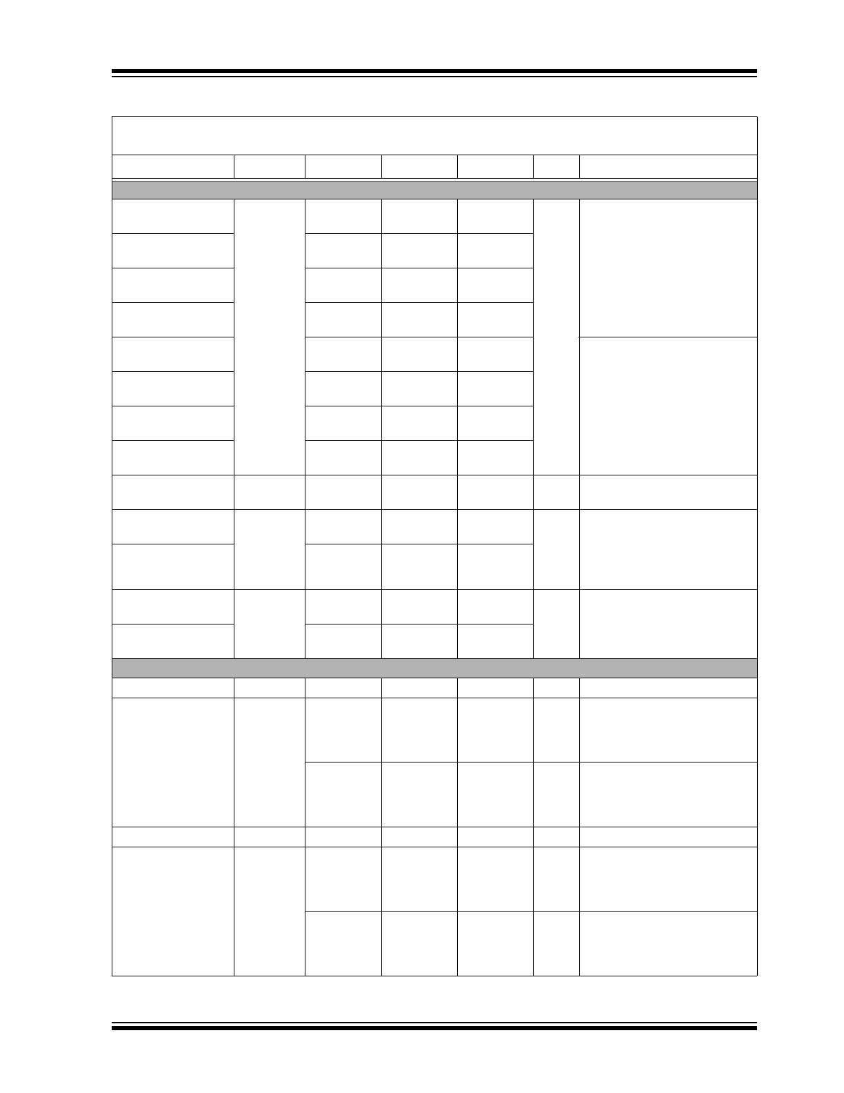
HV7322
TX Output N-Channel MOSFET on V
NN1
Peak Output Current
IM<1:0> = 00
I
OUT_N1
CWEN = 0
—
-0.42
-0.3
A
V
NN1
= -25V, R
L
= 1.0
to
GND
20 ns pulse width at the duty
cycle
D% = 0.1%,
Note 1
Peak Output Current
IM<1:0> = 01
—
-0.8
-0.6
Peak Output Current
IM<1:0> = 10
—
-1.16
-0.9
Peak Output Current
IM<1:0> = 11
—
-1.51
-1.3
Peak Output Current
IM<1:0> = 00
—
-0.5
-0.35
V
NN1
= -60V, R
L
= 1.0
to
GND
20 ns pulse width at the duty
cycle
D% = 0.1%,
Note 1
Peak Output Current
IM<1:0> = 01
—
-1.0
-0.7
Peak Output Current
IM<1:0> = 10
—
-1.5
-1.25
Peak Output Current
IM<1:0> = 11
—
-1.9
-1.6
On-Resistance
IM<1:0> = 11
R
ON_N1
CWEN = 0
—
8.3
10
I
DS
= 100 mA,
Note 1
Peak Output Current
IM<1:0> = X0
I
OUT_N1
CWEN = 1
—
-212
-180
mA
V
NN1
= -10V, R
L
= 1.0
to
GND
20 ns pulse width at the duty
cycle
D% = 0.1%,
Note 1
Peak Output Current
IM<1:0> = X1
—
-386
-340
CW On-Resistance
IM<1:0> = X0
R
ON_N1
CWEN = 1
—
42
48
I
DS
= 100 mA,
Note 1
CW On-Resistance
IM<1:0> = X1
—
17
19
TX Damping MOSFET on
GND
On-Resistance
R
ON_PDMP
—
9
14
I
SD
= 100 mA,
Note 1
B-Mode Peak
Output Current
(
1
)
I
OUT_PDMP
1.15
1.57
—
A
R
L
= 1.0
at TX to
V
NN0
= - 25V
20 ns pulse width at
D% = 0.1%,
Note 1
1.35
1.9
—
A
R
L
= 1.0
at TX to
V
NN0
= - 80V
20 ns pulse width at
D% = 0.1%,
Note 1
On-Resistance
R
ON_NDMP
—
7
13
I
DS
= 100 mA,
Note 1
B-Mode Peak
Output Current
(
1
)
I
OUT_NDMP
—
–1.56
–1.15
A
R
L
= 1.0
at TX to
V
PP0
= +25V
20 ns pulse width at
D% = 0.1%,
Note 1
—
–2.02
–1.6
A
R
L
= 1.0Ω at TX to
V
PP0
= +80V
20 ns pulse width at
D% = 0.1%,
Note 1
ELECTRICAL CHARACTERISTICS (CONTINUED)
Electrical specifications: V
LL
= +2.5V, V
DD
= +5.0V, V
PP0
= +80V, V
NN0
= -80V, V
PP1,2
= +60V, V
NN1,2
= –60V,
V
GP
= +10V, V
GN
= -10V, V
SUB
= 0V, MODE = 0, OEN = REN = 1, T
A
= 25°C.
Parameter
Sym.
Min.
Typ.
Max.
Unit
Conditions
Note 1: Characterized only; not 100% tested in production.
2: Design guidance only.
HV7322
DS20005920A-page 10
2017 Microchip Technology Inc.
RTZSW Auto Bleed High-Voltage Analog Switch
RTZSW
On-Resistance
R
RTZSW
—
152
164
I
RTZSW
= ±1.0 mA,
Note 1
RTZSW to GND
Bleed Resistors
R
b1
18
20
22
k
Note 1
RTZSW Off
Withstand Voltage
V
RTZSW
-80
—
+80
V
I
RTZSW
= ±100 μA,
Note 1
TX OUTPUT Isolation Diodes and Bleed Resistor
Diode Forward
Voltage
V
F
—
1.2
1.9
V
I
FM
= 300 mA,
Note 2
Forward
Continuous Current
I
FM
—
250
—
mA
Note 2
Peak Forward
Pulse Current
I
FSM
—
3.0
—
A
PW = 50 ns,
Note 2
Total Capacitance of
2-Diode
C
T
—
3.2
4
pF
At 1 MHz, 1 dBm, 0V DC,
Note 2
TRSW, LVSW and RXDMP Switches
TRSW and LVSW
Switch-On Resistor
R
TRSW
—
13
18
I
TRSW
= ±1.0 mA,
Note 1
TRSW Off
Withstand Voltage
V
TRSW
-80
—
+80
V
I
SW
= ±100 μA,
Note 1
LVSW Off
Withstand Voltage
V
LVSW
-5.0
—
+5.0
V
I
SW
= ±10 μA,
Note 1
RX to GND
Protection Diode
V
F
—
1
1.2
V
I
F
= ±20 mA,
Note 1
RXDMP Switch
On-Resistance
R
RXDMP
—
14
19
I
SD
= ±1.0 mA,
Note 1
RX0~7 Pin to GND
Bleed Resistor
R
b2
13
20
27
k
Note 2
RX Pin to GND
Capacitance
C
RXG
—
20
22
pF
1 MHz, 1 dBm, 0V DC,
Note 2
Built-In Gate Drive Voltage Linear Regulators
Output P-Channel
Gate Drive Voltage
Referenced to V
PP0
V
PF0
–5.2
–4.5
–4.1
V
V
GN
- V
PP0
< –10V
Output P-Channel
Gate Drive Voltage
Referenced to V
PP1
V
PF1
–5.2
–4.5
–4.1
V
V
GN
- V
PP1
< –10V
Output P-Channel
Gate Drive Voltage
Referenced to V
PP2
V
PF2
–5.2
–4.5
–4.1
V
V
NN0
- V
PP2
< –10V
Output N-Channel
Gate Drive Voltage
Referenced to V
NN0
V
NF0
3.6
4.4
5.2
V
V
GP
- V
NN0
> 10V
ELECTRICAL CHARACTERISTICS (CONTINUED)
Electrical specifications: V
LL
= +2.5V, V
DD
= +5.0V, V
PP0
= +80V, V
NN0
= -80V, V
PP1,2
= +60V, V
NN1,2
= –60V,
V
GP
= +10V, V
GN
= -10V, V
SUB
= 0V, MODE = 0, OEN = REN = 1, T
A
= 25°C.
Parameter
Sym.
Min.
Typ.
Max.
Unit
Conditions
Note 1: Characterized only; not 100% tested in production.
2: Design guidance only.