
2016 Microchip Technology Inc.
DS20005626A-page 1
HV6810
Features
• High Output Voltage 80V
• High-speed 5 MHz at 5 V
DD
• Low-power I
BB
≤ 0.1 mA (All High)
• Active Pull-down 100 µA Minimum at 25°C
• Output Source Current 25 mA at 60V V
BB
• 10-channel Display Driver
• High-speed Serially-shifted Data Input
• 5V CMOS-compatible Inputs
• Latches on all Driver Outputs
• Pin-compatible Replacement for UCN5810A,
TL4810A and TL4810B
Applications
• High-speed Dot Matrix Print Head Driver
• Vacuum Fluorescent Display (VFD) Driver
General Description
The HV6810 is a monolithic integrated circuit designed
to drive a dot matrix or segmented VFD. These devices
feature a serial data output to cascade additional
devices for large displays.
A 10-bit data word is serially loaded into the shift
register on the positive-going transition of the clock.
Parallel data are transferred to the output buffers
through a 10-bit D-type latch while the latch enable
input is high. The data are latched when the latch
enable is low. When the blanking input is high, all of the
outputs are low.
Outputs are structures formed by double-diffused MOS
(DMOS) transistors with output voltage ratings of 80V
and 25 mA source-current capability. All inputs are
compatible with CMOS levels.
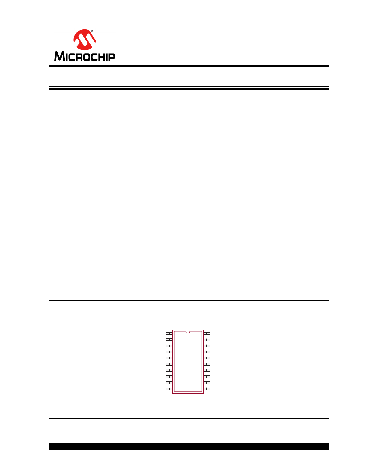
Package Type
See
Table 2-1
for pin information.
20-lead SOW
(Top view)
1
20
10-Channel Serial-Input Latched Display Driver
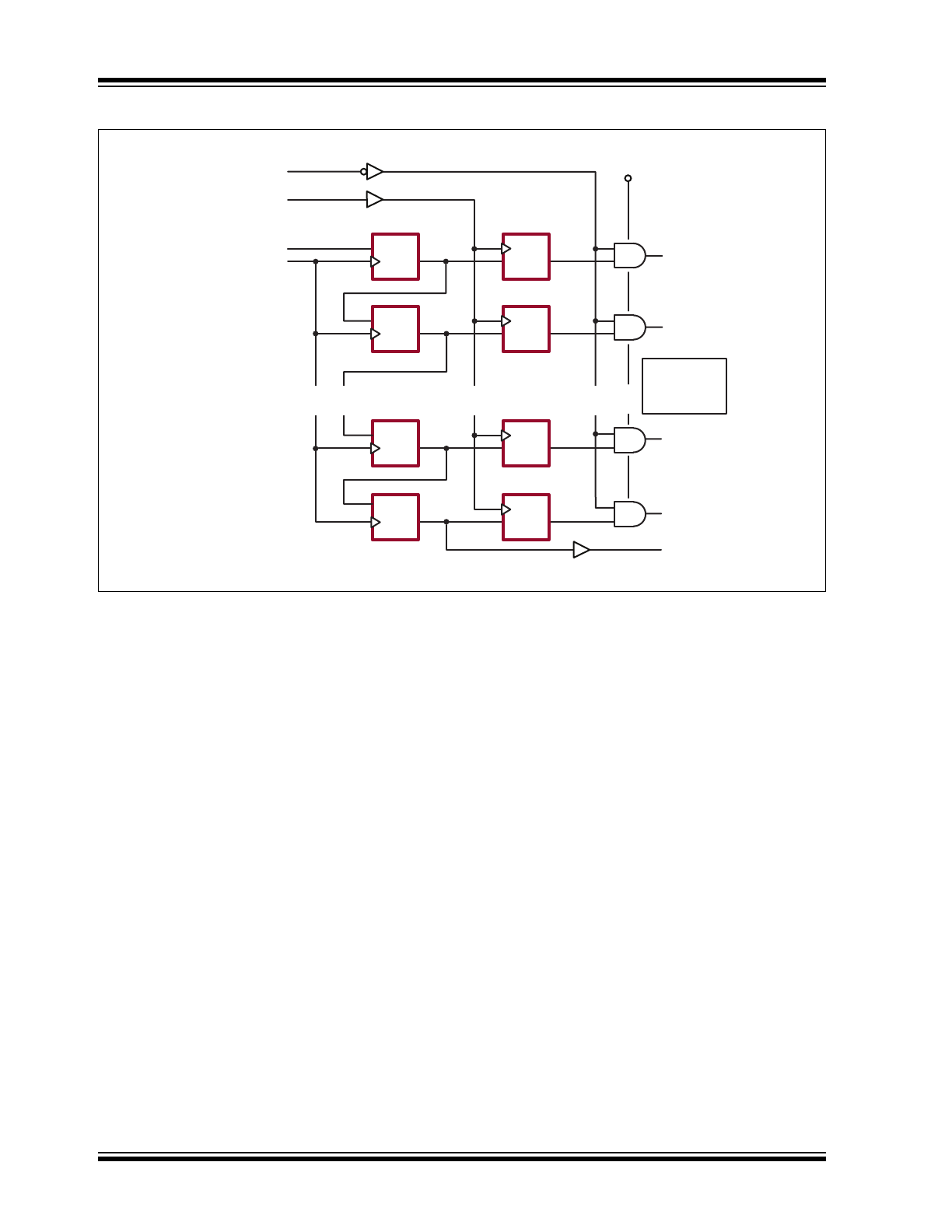
Blanking
Latch Enable
Q1
Q9
Q2
Q10
1D
C1
Data Input
Clock
LC1
LC2
LC9
LC10
Latches
Shift Register
•
•
•
6 Stages
(Q3 thru Q8
not shown
Serial
Out
C2
2D
1D
C1
1D
C1
1D
C1
•
•
•
•
•
•
•
•
•
C2
2D
C2
2D
C2
2D
•
•
•
V
BB
HV6810
DS20005626A-page 2
2016 Microchip Technology Inc.
Functional Block Diagram
2016 Microchip Technology Inc.
DS20005626A-page 3
HV6810
1.0
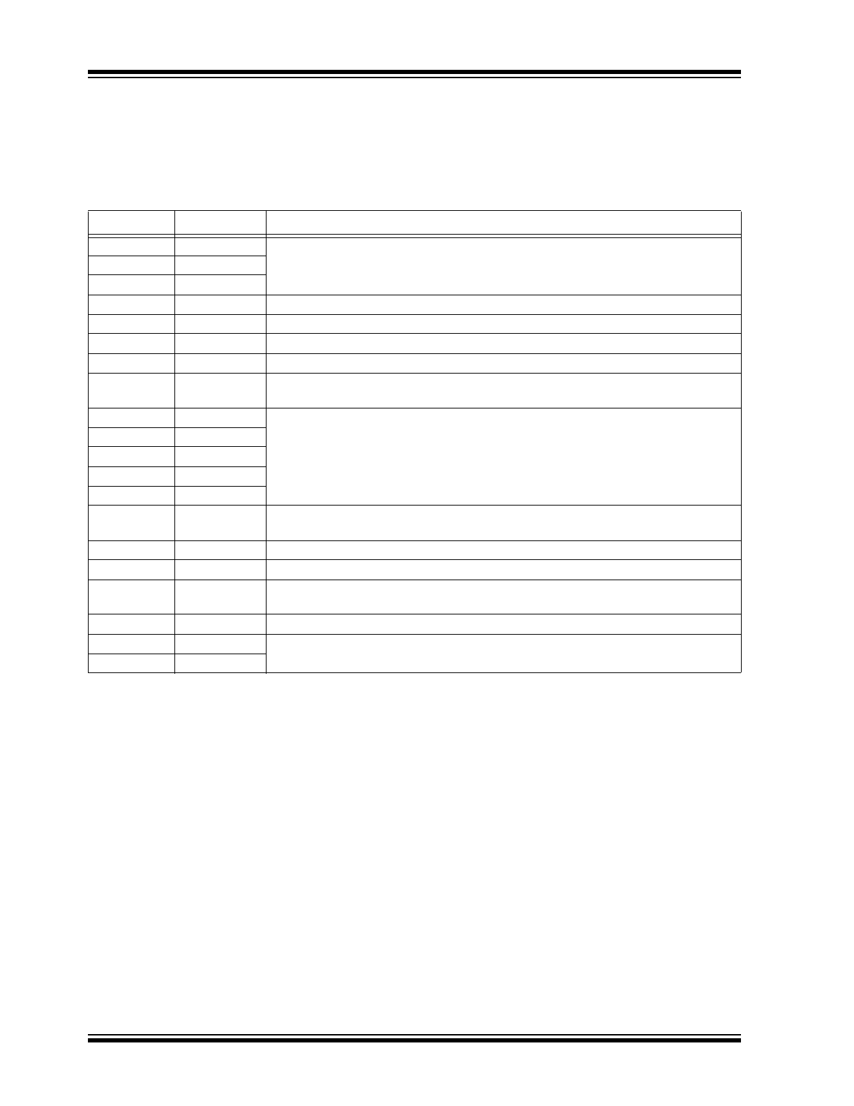
ELECTRICAL CHARACTERISTICS
Absolute Maximum Ratings† (
Note 1
)
Logic Supply Voltage, V
DD
(
Note 2
)......................................................................................................................... 7.5V
Driver Supply Voltage, V
BB
(
Note 2
) ......................................................................................................................... 90V
Output Voltage (
Note 2
)
........................................................................................................................................... 90V
Input Voltage (
Note 2
)
......................................................................................................................–0.3V to V
DD
+0.3V
Operating Ambient Temperature, T
A
.......................................................................................................–45°C to +85°C
Continuous Total Power Dissipation at 25°C Free-air Temperature:
20-lead SOW (
Note 3
) .......................................................................................................................... 1500 mW
† Notice: Stresses above those listed under “Absolute Maximum Ratings” may cause permanent damage to the
device. This is a stress rating only, and functional operation of the device at those or any other conditions above those
indicated in the operational sections of this specification is not intended. Exposure to maximum rating conditions for
extended periods may affect device reliability.
Note 1:
Over operating free-air temperature
2:
All voltages are referenced to V
SS
.
3:
For operations above 25°C ambient, derate linearly to 85°C at 15 mW/°C.
RECOMMENDED OPERATING CONDITIONS
Parameter
Sym.
Min.
Typ.
Max.
Unit
Conditions
Logic Supply Voltage
V
DD
4.5
—
5.5
V
High Supply Voltage
V
BB
20
—
80
V
Supply Voltage
V
SS
—
0
—
V
High-level Input Voltage
(for V
DD
= 5V)
V
IH
3.5
—
5.3
V
Low-level Input Voltage
V
IL
–0.3
—
0.8
V
Continuous High-level Q Output
Current
I
OH
25
—
—
mA
Clock Frequency
f
CLK
—
—
5
MHz
Operating Ambient Temperature
T
A
–40
—
+85
°C
DC ELECTRICAL CHARACTERISTICS
Electrical Specifications: V
DD
= 5V, V
BB
= 60V, V
SS
= 0V and T
A
= 25°C unless otherwise noted.
Parameter
Sym.
Min.
Typ.
Max
Unit
Conditions
High-level Output
Voltage
Q Outputs
V
OH
57.5
58
—
V
I
O
= +25 mA
Serial Output
4
4.5
—
V
DD
= +4.5V, I
OL
= +100 µA
Low-level Output
Voltage
Q Outputs
V
OL
—
0.15
1
V
I
O
= –100 µA,
blanking input at V
DD
Serial Output
—
0.05
0.1
V
DD
= +4.5V, I
O
= –100 µA
Low-level Q Output Current
(Pull-down Current)
I
OL
60
80
—
µA
T
A
= Max, V
OL
= +0.7V
(
Note 1
)
Off-state Output Current
I
O(OFF)
—
–1
–15
µA
V
O
= 0V, blanking input at V
DD
(
Note 1
)
High-level Input Current
I
IH
—
—
1
µA
V
lN
= V
DD
Supply Current from V
DD
(Standby)
I
DD
—
10
50
µA
All inputs at 0V,
one Q output high
—
10
50
All inputs at 0V,
all Q outputs low
Note 1: All typical values are at T
A
= 25°C except for I
OL
and I
O(OFF)
.
HV6810
DS20005626A-page 4
2016 Microchip Technology Inc.
Supply Current from V
BB
I
BB
—
0.05
0.1
mA
All outputs low,
all Q outputs open
—
0.05
0.1
All outputs high,
all Q outputs open
AC ELECTRICAL CHARACTERISTICS
Electrical Specifications: Timing requirements are over the recommended operating conditions.
Parameter
Sym.
Min.
Typ.
Max
Unit
Conditions
Pulse Duration, Clock High
t
W(CKH)
100
—
—
ns
Pulse Duration, Latch Enable High
t
W(LEH)
100
—
—
ns
Setup Time, Data before Clock
t
SU(D)
50
—
—
ns
Hold Time, Data after Clock
t
H(D)
50
—
—
ns
Delay Time, Clock to Latch Enable
High
t
CKH-LEH
50
—
—
ns
Propagation Delay Time, Latch Enable
to Output
t
PD
—
300
—
ns
Note 1
Note 1: Switching characteristics, V
BB
= 60V, T
A
= 25°C
TEMPERATURE SPECIFICATIONS
Parameter
Sym.
Min.
Typ.
Max.
Unit
Conditions
TEMPERATURE RANGE
Operating Ambient Temperature
T
A
–40
—
+85
°C
PACKAGE THERMAL RESISTANCE
20-lead SOW
JA
—
66
—
°C/W
DC ELECTRICAL CHARACTERISTICS (CONTINUED)
Electrical Specifications: V
DD
= 5V, V
BB
= 60V, V
SS
= 0V and T
A
= 25°C unless otherwise noted.
Parameter
Sym.
Min.
Typ.
Max
Unit
Conditions
Note 1: All typical values are at T
A
= 25°C except for I
OL
and I
O(OFF)
.
2016 Microchip Technology Inc.
DS20005626A-page 5
HV6810
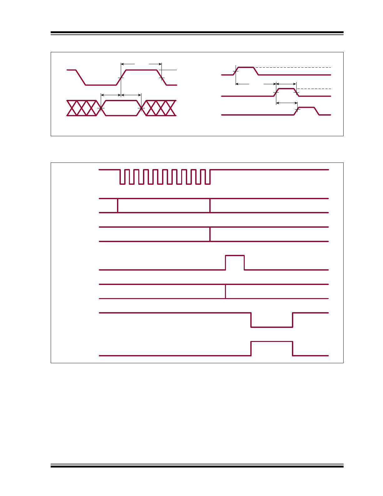
Switching Waveforms
t
W(CKH)
50%
50%
V
IH
V
IL
V
IH
V
IL
Valid
50%
50%
Data
Clock
t
H(D)
t
SU(D)
50%
50%
50%
t
CKH-LEH
Valid
Valid
90%
Clock
Input
Latch
Enable
Q Output
t
PD
t
W(LEH)
Input Timing
V
IH
V
IL
V
IH
V
IL
V
OH
V
OL
Output Switching Timing
Timing Diagram
VALID
IRRELEVANT
INVALID
VALID
PREVIOUSLY STORED DATA NEW DATA VALID
VALID
Clock
Data In
SR Contents
Latch
Enable
Latch
Contents
Blanking
Q Outputs
HV6810
DS20005626A-page 6
2016 Microchip Technology Inc.
2.0
PIN DESCRIPTION
The details on the pins of HV6810 are listed on
Table 2-1
. Refer to
Package Type
for the location of
pins.
TABLE 2-1:
PIN FUNCTION TABLE
Pin Number
Pin Name
Description
1
Q8
High-voltage output
2
Q7
3
Q6
4
CLOCK
Input data are shifted into the data shift register on the positive edge of the clock.
5
VSS
Usually V
SS
= 0V; ground connection
6
N/C
No connection
7
VDD
Low-voltage power supply
8
LE (STROBE)
When LE is high, the shift register output is latched to Q output. When LE stays high,
the latches are in Transparent mode.
9
Q5
High-voltage output
10
Q4
11
Q3
12
Q2
13
Q1
14
BLANKING
When blanking is high, all Q's are forced to a Low state regardless of data in each
channel.
15
DATA IN
Input data for the input shift register
16
VBB
High-voltage power supply
17
SERIAL DATA
OUT
Output data from the shift register
18
N/C
No connection
19
Q10
High-voltage output
20
Q9
2016 Microchip Technology Inc.
DS20005626A-page 7
HV6810
3.0
FUNCTIONAL DESCRIPTION
Follow the steps below to power up and power down
the HV6810.
POWER-UP AND POWER-DOWN SEQUENCE
1
Power-up
Power-down
Step
Description
Step
Description
1
Connect ground V
SS
.
1
Remove V
BB
.
2
Apply V
DD
.
2
Remove all inputs.
3
Set all inputs (Data, CLK, Enable, etc.) to a
known state.
3
Remove V
DD
.
4
Apply V
BB
.
4
Disconnect ground V
SS
.
Note 1: The V
BB
should not drop below V
DD
or float during operation.
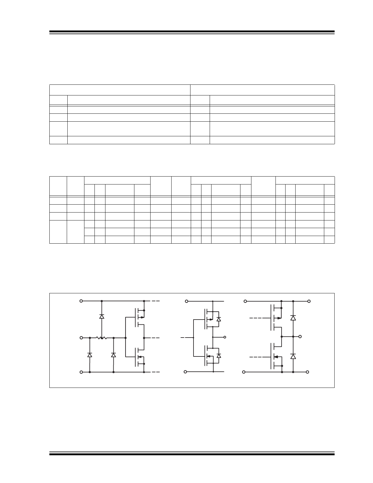
FUNCTION TABLE
1
Serial
Data
Input
Clock
Input
Shift Register Contents
Serial
Data
Output
LE
Strobe
Input
Latch Contents
Blanking
Input
Output Contents
I
1
I
2
I
3
... I
N-1
I
N
I
1
I
2
I
3
... I
N-1
I
N
I
1
I
2
I
3
... I
N-1
I
N
H
L to H
H
R
1
R
2
...R
N–2
R
N–1
R
N–1
—
—
—
—
—
—
—
—
—
—
L
L to H
L
R
1
R
2
...R
N–2
R
N–1
R
N–1
—
—
—
—
—
—
—
—
—
—
X
H to L R
1
R
2
R
3
...R
N–1
R
N
R
N
—
—
—
—
—
—
—
—
—
—
—
—
X
X
X...X
X
X
L
R
1
R
2
R
3
...R
N–1
R
N
—
—
—
—
—
P
1
P
2
P
3
...P
N–1
P
N
P
N
H
P
1
P
2
P
3
...P
N–1
P
N
L
P
1
P
2
P
3
...P
N–1
P
N
—
—
—
—
—
—
X
X
X...X
X
H
L
L
L...L
L
Note 1:
L = Low logic level
H = High logic level
X = Don’t care
P = Present state
R = Previous state
,
VDD
DATA
INPUT
VSS
Input Equivalent Circuit
VDD
GND
DATA
OUT
VSS
Q
Logic Data Output
VBB
High Voltage Output
FIGURE 3-1:
Input and Output Equivalent Circuits.
HV6810
DS20005626A-page 8
2016 Microchip Technology Inc.
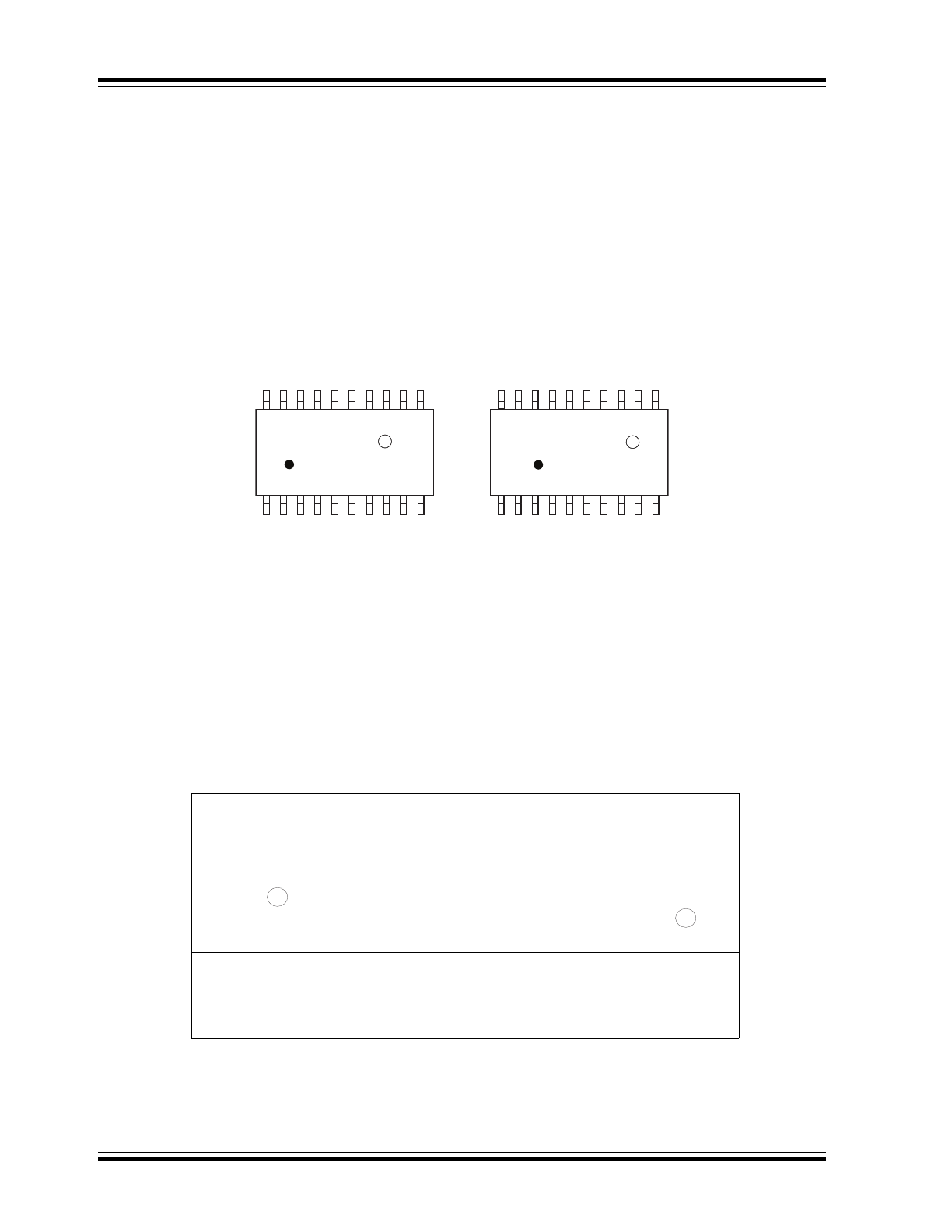
4.0
PACKAGE MARKING INFORMATION
4.1
Packaging Information
Legend: XX...X
Product Code or Customer-specific information
Y
Year code (last digit of calendar year)
YY
Year code (last 2 digits of calendar year)
WW
Week code (week of January 1 is week ‘01’)
NNN
Alphanumeric traceability code
Pb-free JEDEC
®
designator for Matte Tin (Sn)
*
This package is Pb-free. The Pb-free JEDEC designator ( )
can be found on the outer packaging for this package.
Note:
In the event the full Microchip part number cannot be marked on one line, it will
be carried over to the next line, thus limiting the number of available
characters for product code or customer-specific information. Package may or
not include the corporate logo.
3
e
3
e
20-lead SOW
Example
HV6810WG
e3
1624965
XXXXXXX
e3
YYWWNNN
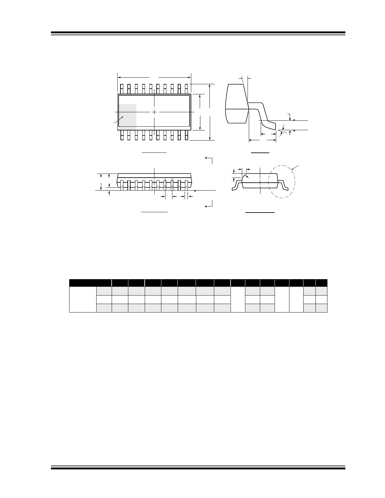
20-Lead SOW (Wide Body) Package Outline (WG)
12.80x7.50mm body, 2.65mm height (max), 1.27mm pitch
Symbol
A
A1
A2
b
D
E
E1
e
h
L
L1
L2
ș
ș
Dimension
(mm)
MIN
2.15*
0.10
2.05
0.31
12.60*
9.97*
7.40*
1.27
BSC
0.25
0.40
1.40
REF
0.25
BSC
0
O
5
O
NOM
-
-
-
-
12.80
10.30
7.50
-
-
-
-
MAX
2.65
0.30
2.55*
0.51
13.00* 10.63*
7.60*
0.75
1.27
8
O
15
O
JEDEC Registration MS-013, Variation AC, Issue E, Sep. 2005.
7KLVGLPHQVLRQLVQRWVSHFL¿HGLQWKH-('(&GUDZLQJ
Drawings are not to scale.
D
Seating
Plane
Gauge
Plane
L
L1
L2
Top View
Side View
View A - A
View B
View
B
θ1
θ
E1
E
A A2
A1
A
A
Seating
Plane
e
b
h
h
20
1
Note 1
Note 1
(Index Area
0.25D x 0.75E1)
Note:
1.
$3LQLGHQWL¿HUPXVWEHORFDWHGLQWKHLQGH[DUHDLQGLFDWHG7KH3LQLGHQWL¿HUFDQEHDPROGHGPDUNLGHQWL¿HUDQHPEHGGHGPHWDOPDUNHURU
a printed indicator.
Note: For the most current package drawings, see the Microchip Packaging Specification at www.microchip.com/packaging.
Note: For the most current package drawings, see the Microchip Packaging Specification at www.microchip.com/packaging.
2016 Microchip Technology Inc.
DS20005626A-page 9
HV6810

HV6810
DS20005626A-page 10
2016 Microchip Technology Inc.
NOTES: