
2015 Microchip Technology Inc.
DS20005455A-page 1
HV582
Features
• 96 High-Voltage Channels
- Up to 80V Operating Output Voltage
- 75 mA Peak Output Sink/Source Current
• Six Parallel 16-bit Shift Registers
- Clockwise and Counter-Clockwise Data
Shifting via DIR Pin
• 30 MHz Data Rate
Applications
• Inkjet Printer Driver
• AC Plasma Data Driver
• 3D Printer Driver
Related Devices
• HV583: 128-Channel Serial to Parallel Converter
with Push-Pull Outputs
Description
HV582 is a unipolar, 96-channel low-voltage serial to
high-voltage parallel converter with push-pull outputs.
This device has been designed for applications requiring
multiple high-voltage outputs with current sinking and
sourcing capabilities, such as plasma displays and Inkjet
printers.
The device consists of six parallel 16-bit shift registers,
a 96-bit latch and 96 high-voltage outputs. The shift
registers operate at 30 MHz, allowing 180 MHz data
rates due to the parallel arrangement.
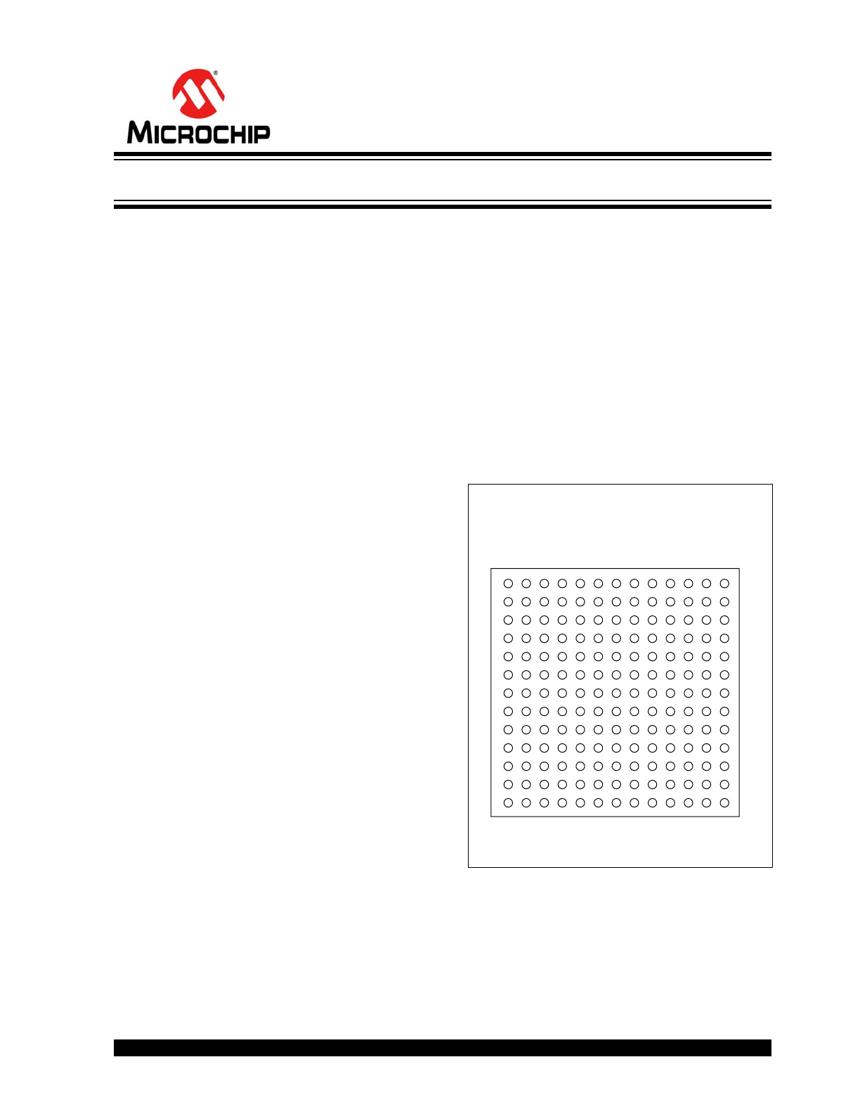
HV582 is offered in a 169-ball 10 x 10 x 1.1 mm
TFBGA package.
Package Type
* See
Section 2.0, Package Pin Configuration and
Function Description
.
HV582
10x10x1.1 mm TFBGA*
Bottom View
6
7
8
9
10
5
4
1
2
3
11
12
13
H
G
F
E
D
J
K
N
M
L
C
B
A
96-Channel Serial to Parallel Converter with Push-Pull Outputs
HV582
DS20005455A-page 2
2015 Microchip Technology Inc.
Block Diagram
96-Bit
Latch
HV
OUT
1
D1A
CLK
Level
Translator
16-Bit
Shift
Register
16-Bit
Shift
Register
16-Bit
Shift
Register
16-Bit
Shift
Register
16-Bit
Shift
Register
16-Bit
Shift
Register
D1B
D2A
D2B
D3A
D3B
D4A
D4B
D5A
D5B
D6A
D6B
DIR
LE
RST
OL
POL
OE
OH
Level
Translator
D1
D16
D65
D80
D17
D32
D33
D48
D49
D64
D81
D96
LD1
LD96
Decoder
Decoder
V
PP
HV
GND
V
PP
HV
GND
HV
OUT
96
V
DD
HV
GND
GND
2015 Microchip Technology Inc.
DS20005455A-page 3
HV582
1.0
ELECTRICAL
CHARACTERISTICS
Absolute Maximum Rating†
Supply Voltage V
DD
.................................................................................................................................... -0.5V to +6.0V
High-Voltage Supply V
PP
.............................................................................................................................. V
DD
to +85V
Logic Input Voltages...........................................................................................................................-0.5V to V
DD
+ 0.5V
Operating Junction Temperature............................................................................................................. -40°C to +125°C
Storage Temperature .............................................................................................................................. -65°C to +150°C
†Notice: Stresses above those listed under “Absolute Maximum Ratings” may cause permanent damage to the
device. This is a stress rating only and functional operation of the device at those or any other conditions, above those
indicated in the operational listings of this specification, is not implied. Exposure to maximum rating conditions for
extended periods may affect device reliability. Device is ESD sensitive. Use appropriate ESD precaution.
RECOMMENDED OPERATING CONDITIONS
Parameter
Symbol
Min.
Typ.
Max.
Units
Conditions
Logic Supply Voltage
V
DD
4.5
5.0
5.5
V
High-Voltage Supply
V
PP
10
—
80
V
High-Level Input Voltage
V
IH
V
DD
– 0.9
—
V
DD
V
Low-Level Input Voltage
V
IL
0
—
0.9
V
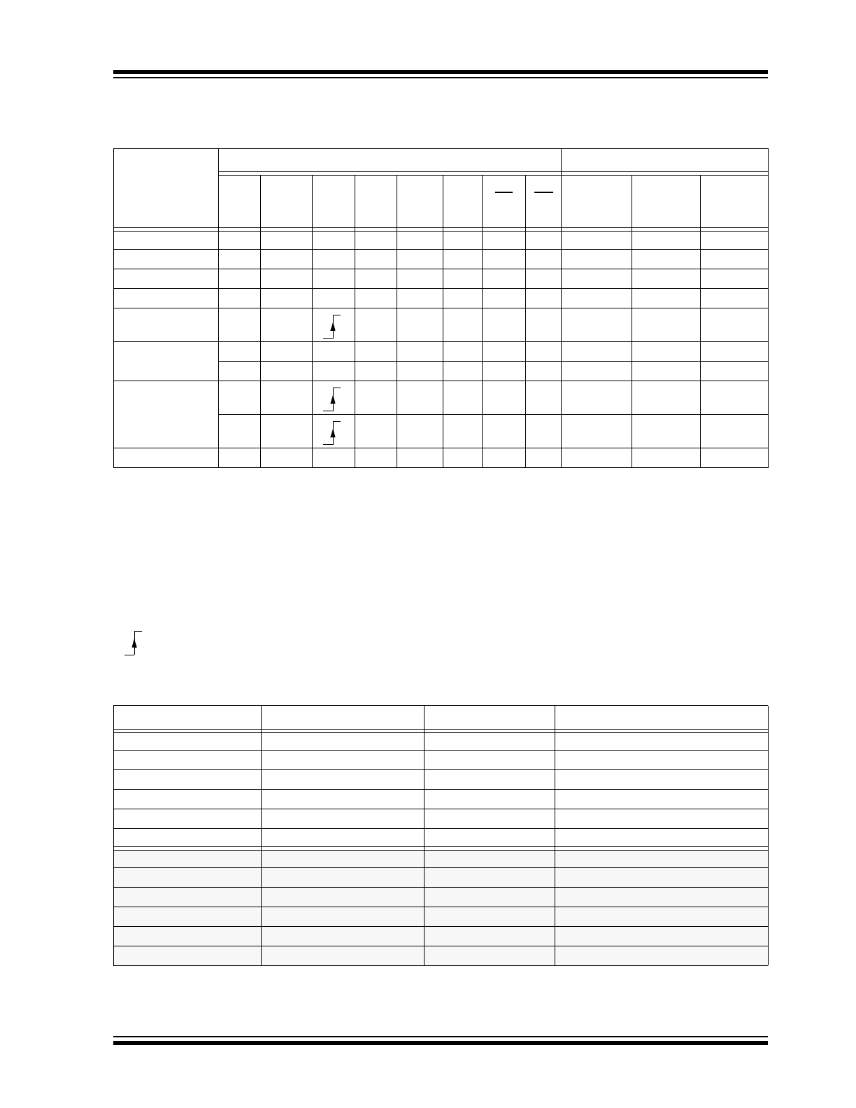
TABLE 1-1:
POWER SEQUENCES
Sequence Type
Steps
Power-Up Sequence
1.
Connect Ground.
2.
Apply V
DD
.
3.
Set All Inputs (Data, CLK, etc.) to a known state.
4.
Apply V
PP
.
Power-Down Sequence
Repeat the Power-Up sequence in reverse order.
DC ELECTRICAL CHARACTERISTICS
Electrical Specification: Unless otherwise specified, T
A
= T
J
= +25°C, V
DD
= 5.0V and V
PP
= 80V.
Parameter
Symbol
Min.
Typ.
Max.
Units
Conditions
V
PP
Quiescent Supply Current
I
PPQ
–
–
100
µA
V
DD
Quiescent Supply Current
I
DDQ
–
–
100
µA
V
DD
Supply Current
I
DD
–
–
25
mA
f
CLK
= 30 MHz,
LE = low
High-Level Output Voltage
HV
OH
70
75
–
V
I
OUT
= 75 mA,
V
PP
= 80V
Output P-Channel Body Diode
HV
OHD
–
–
83
V
I
OUT
= -75 mA,
V
PP
= 80V (
Note 1
)
Low-Level Output Voltage
HV
OL
–
5.0
10
V
I
OUT
= -75 mA
Output N-Channel Body Diode
HV
OLD
-3.0
–
–
V
I
OUT
= 75 mA (
Note 1
)
Logic Input High Current
I
IH
–
–
1.0
µA
V
IH
= V
DD
10
30
50
V
IH
= V
DD,
RST and POL only
Note 1:
Specification is for design guidance only.
HV582
DS20005455A-page 4
2015 Microchip Technology Inc.
Logic Input Low Current
I
IL
-1.0
–
–
µA
V
IL
= -0.3V
Logic Output High
V
OH
3.5
–
–
V
I
OUT
= 4 mA
Logic Output Low
V
OL
–
–
1.0
I
OUT
= -4 mA
DC ELECTRICAL CHARACTERISTICS (CONTINUED)
Electrical Specification: Unless otherwise specified, T
A
= T
J
= +25°C, V
DD
= 5.0V and V
PP
= 80V.
Parameter
Symbol
Min.
Typ.
Max.
Units
Conditions
Note 1:
Specification is for design guidance only.
AC ELECTRICAL CHARACTERISTICS
Electrical Characteristics: Unless otherwise specified T
A
= T
J
= +25°C, V
DD
= 5.0V and V
PP
= 80V.
Parameter
Symbol
Min.
Typ.
Max.
Units
Conditions
Data Clock Frequency
f
CLK
—
—
30
MHz
Clock Pulse Width, High and Low
t
wCLK
16.6
—
—
ns
Note 1
LE Pulse Width, High and Low
t
wLE
16.6
—
—
Note 2
Setup Time, DnA/B to CLK
t
su1
5
—
—
Note 1
Setup Time, CLK to LE
t
su2
15
—
—
Note 1
Setup Time, LE to OL,OH
t
su3
25
—
—
Note 1
Hold Time, CLK to DnA/B
t
h1
15
—
—
Note 1
Hold Time, LE to CLK
t
h2
15
—
—
Note 1
CLK to DnA/B
(High-to-Low)
t
pdHL
—
—
25
C
L
= 170 pF
CLK to DnA/B (Low-to-High)
t
pdLH
—
—
25
C
L
= 170 pF
LE,OL,OH to HV
OUT
n
(High-to-Low)
t
pHL
—
—
300
C
L
= 170 pF
LE,OL,OH to HV
OUT
n
(Low-to-High)
t
pLH
—
—
300
C
L
= 170 pF
OE to HV
OUT
n (High-to-Low)
t
pHZL
—
—
150
C
L
= 170 pF
OE to HV
OUT
n (Low-to-High)
t
pLZH
—
—
150
C
L
= 170 pF
OE to HV
OUT
n (High-to-Low)
t
pHZ
—
—
300
OE to HV
OUT
n (Low-to-High)
t
pLZ
—
—
300
Rise Time HV
OUT
n
t
r
—
—
200
C
L
= 170 pF
Fall Time HV
OUT
n
t
f
—
—
200
C
L
= 170 pF
Note 1:
Specification is obtained by characterization and is not 100% tested.
2:
Specification is for design guidance only.
TEMPERATURE SPECIFICATIONS
Parameters
Sym.
Min.
Typ.
Max.
Units
Conditions
Temperature Ranges
Operating Junction Temperature
T
J
-40
—
+125
°C
Storage Temperature
T
A
-65
—
+150
°C
Package Thermal Resistance
Thermal Resistance, 169-Ball TFBGA
JA
—
27
—
°C/W
2015 Microchip Technology Inc.
DS20005455A-page 5
HV582
1.1
Logic Characteristics
TABLE 1-2:
LOGIC FUNCTION TRUTH TABLE
Function
Inputs
Outputs
RST
Data
CLK
LE
OE
POL
OL
OH
Shift Reg.
1 2...96
HV
Outputs
1 2...96
Data Out
All Low
L
X
X
X
H
X
L
X
* *...*
L L...L
*
All High
L
X
X
X
H
X
H
L
* *...*
H H...H
*
Output High Z
L
X
X
X
L
X
X
X
* *...*
Z Z...Z
*
Invert Mode
L
X
X
L
H
H
H
H
* *...*
* *...*(b)
*
Load S/R
L
H or L
L
H
L
H
H
H or L *...*
* *...*
*
Store Data
in Latches
L
X
X
L
H
L
H
H
* *...*
* *...*
*
L
X
X
L
H
H
H
H
* *...*
* *...* (b)
*
Transparent
Mode
L
L
H
H
L
H
H
L * *...*
L * *...*
*
L
H
H
H
L
H
H
H * *...*
H * *...*
*
Reset
H
X
X
X
H
L
H
H
L * *...*
L * *...*
L
Legend:
D
= Data
H
= Level High
L
= Level Low
X
= Don’t Care
Z
= High Impedance
b
= Inversion
*
= Dependent of previous stage’s state before the last CLK or last LE high
= Low-to-High Transition
TABLE 1-3:
OUTPUT SHIFT OPERATION
Input
Output
DIR
Shift Operation
D1A
D1B
L
D1 to D16
D2A
D2B
L
D17 to D32
D3A
D3B
L
D33 to D48
D4A
D4B
L
D49 to D64
D5A
D5B
L
D65 to D80
D6A
D6B
L
D81 to D96
D1B
D1A
H
D16 to D1
D2B
D2A
H
D32 to D17
D3B
D3A
H
D48 to D33
D4B
D4A
H
D64 to D49
D5B
D5A
H
D80 to D65
D6B
D6A
H
D96 to D81
HV582
DS20005455A-page 6
2015 Microchip Technology Inc.
1.2
Timing Diagram
1.3
Input and Output Equivalent Circuits
t
wCLK
t
wCLK
t
h1
t
su1
t
su1
t
h1
t
pdLH
t
pdHL
t
su2
t
h2
t
wLE
t
wLE
50%
50%
50%
50%
50%
50%
50%
50%
50%
50%
t
su3
50%
50%
50%
50%
90%
10%
90%
10%
10%
90%
90%
10%
50%
50%
t
pLH
t
pHZ
t
pLZ
t
pLZH
t
pHZL
t
pHL
t
r
t
f
CLK
DnA/B
(input)
LE
OL, OH
OE
OE
HV
OUT
n
DnA/B
(output)
LE, OH, OL
V
IH
V
IL
V
IH
V
IL
V
OH
V
OL
V
IH
V
IL
V
IH
V
IL
V
IH
V
IL
V
IH
V
IL
V
IH
V
IL
50%
50%
V
OH
V
OL
Logic Data Output
High Voltage Outputs
Logic Inputs
V
DD
Input
GND
V
DD
Data Out
GND
V
PP
HV
GND
HV
OUT
2015 Microchip Technology Inc.
DS20005455A-page 7
HV582
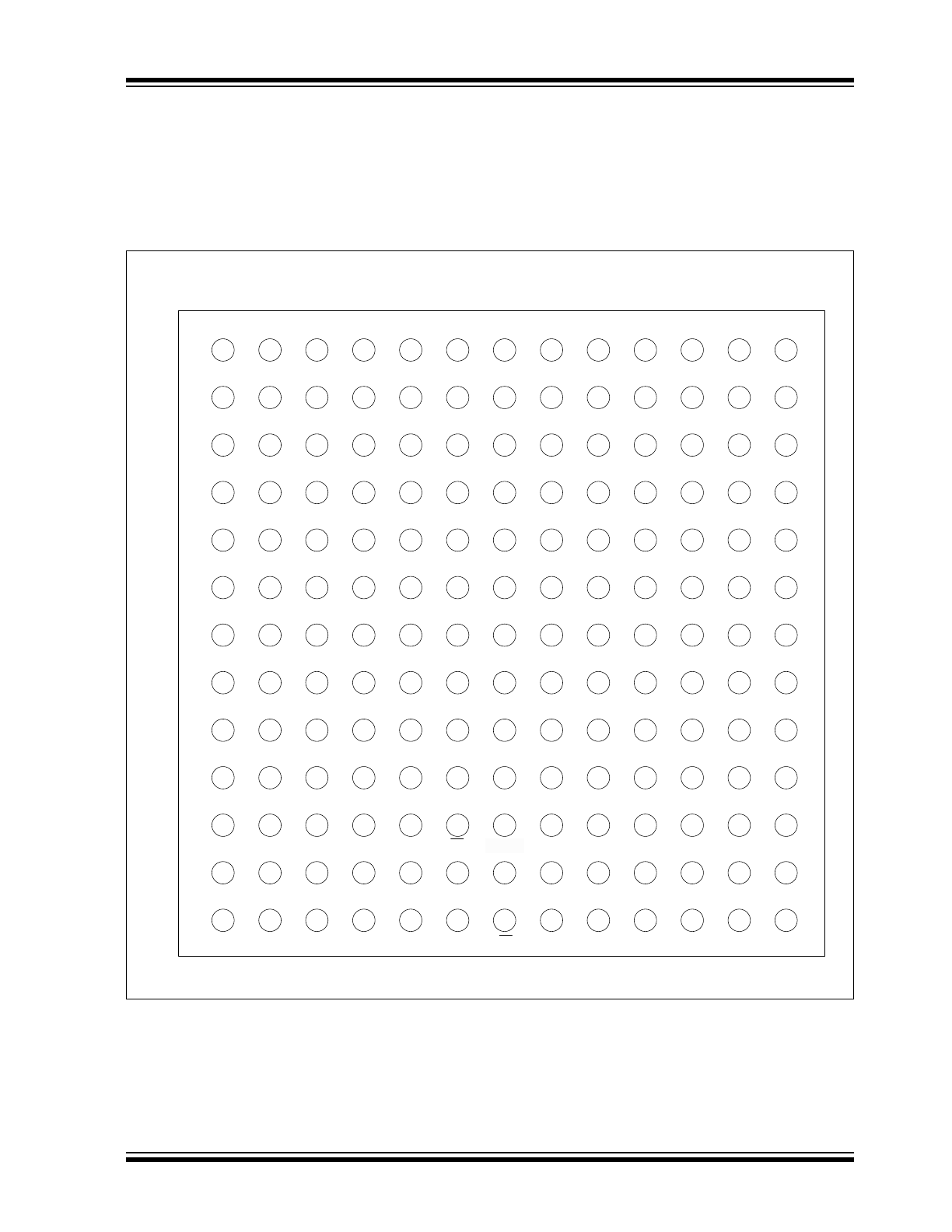
2.0
PACKAGE PIN
CONFIGURATION AND
FUNCTION DESCRIPTION
This section details the pin designation for the 169-Ball
TFBGA package (
Figure 2-1
). The descriptions of the
pins are listed in
Table 2-1
.
FIGURE 2-1:
169-Ball TFBGA Package
8
7
6
5
3
1
0
1
9
4
12
11
3
2
1
H
G
F
E
D
J
K
N
M
L
C
B
A
HV
OUT
94
HV
OUT
96
NC
D6B
D3B
POL
OH
D5A
HV
OUT
3
HV
OUT
5
HV
OUT
6
LE
HV
OUT
93
HV
OUT
95
NC
D5B
D2B
OE
DIR
D4A
HV
OUT
2
HV
OUT
4
HV
OUT
7
CLK
HV
OUT
92
HV
OUT
91
NC
D4B
D1B
OL
RESET
D3A
HV
OUT
1
HV
OUT
8
HV
OUT
9
D6A
HV
OUT
90
HV
OUT
89
HV
OUT
88
NC
V
DD
GND
V
DD
V
H
D
N
G
OUT
10
HV
OUT
11
HV
OUT
12
NC
HV
OUT
87
HV
OUT
86
HV
OUT
85
NC
HV
GND
HV
GND
HV
GND
HV
GND
NC
HV
OUT
13
HV
OUT
14
HV
OUT
15
HV
GND
HV
OUT
84
HV
OUT
83
HV
OUT
82
NC
HV
GND
HV
GND
HV
GND
HV
GND
NC
HV
OUT
16
HV
OUT
17
HV
OUT
18
HV
GND
HV
OUT
81
HV
OUT
80
HV
OUT
79
NC
V
PP
V
PP
V
PP
V
PP
NC
HV
OUT
19
HV
OUT
20
HV
OUT
21
V
PP
HV
OUT
78
HV
OUT
77
HV
OUT
76
NC
V
PP
V
PP
V
PP
V
PP
NC
HV
OUT
22
HV
OUT
23
HV
OUT
24
V
PP
HV
OUT
75
HV
OUT
74
HV
OUT
73
NC
V
PP
V
PP
NC
V
PP
NC
HV
OUT
25
HV
OUT
26
HV
OUT
27
V
PP
HV
OUT
72
HV
OUT
71
HV
OUT
70
NC
NC
NC
NC
NC
NC
HV
OUT
28
HV
OUT
29
HV
OUT
30
NC
HV
OUT
69
HV
OUT
68
HV
OUT
61
HV
OUT
58
HV
OUT
55
HV
OUT
52
HV
OUT
49
HV
OUT
46
HV
OUT
40
HV
OUT
37
HV
OUT
31
HV
OUT
32
HV
OUT
43
HV
OUT
67
HV
OUT
64
HV
OUT
62
HV
OUT
59
HV
OUT
56
HV
OUT
53
HV
OUT
50
HV
OUT
47
HV
OUT
41
HV
OUT
38
HV
OUT
35
HV
OUT
33
HV
OUT
44
HV
OUT
66
HV
OUT
65
HV
OUT
63
HV
OUT
60
HV
OUT
57
HV
OUT
54
HV
OUT
51
HV
OUT
48
HV
OUT
42
HV
OUT
39
HV
OUT
36
HV
OUT
34
HV
OUT
45
NC
NC
D2A
D1A
NC
RST
Top View
HV582
DS20005455A-page 8
2015 Microchip Technology Inc.
TABLE 2-1:
PIN ASSIGNMENT
Pin #
Symbol
Pin #
Symbol
Pin #
Symbol
A1
HV
OUT
66
D3
HV
OUT
70
K6, K8
GND
A2
HV
OUT
65
D4, D5, D6, D7, D8, D9, D10,
E4, E7, E10, F4, F10, G4,
G10, H4, H10, J4, J10, K4,
K9, K10, L3, L10, M3, N3
NC
K11
HV
OUT
10
A3
HV
OUT
63
D11
HV
OUT
28
K12
HV
OUT
11
A4
HV
OUT
60
D12
HV
OUT
29
K13
HV
OUT
12
A5
HV
OUT
57
D13
HV
OUT
30
L1
HV
OUT
92
A6
HV
OUT
54
E1
HV
OUT
75
L2
HV
OUT
91
A7
HV
OUT
51
E2
HV
OUT
74
L4
DB4
A8
HV
OUT
48
E3
HV
OUT
73
L5
DB1
A9
HV
OUT
45
E5, E6, E8, E9, F5, F6, F7,
F8, F9, G5, G6, G7, G8, G9
V
PP
L6
OL
A10
HV
OUT
42
E11
HV
OUT
25
L7
RST
A11
HV
OUT
39
E12
HV
OUT
26
L8
D6A
A12
HV
OUT
36
E13
HV
OUT
27
L9
D3A
A13
HV
OUT
34
F1
HV
OUT
78
L11
HV
OUT
1
B1
HV
OUT
67
F2
HV
OUT
77
L12
HV
OUT
8
B2
HV
OUT
64
F3
HV
OUT
76
L13
HV
OUT
9
B3
HV
OUT
62
F11
HV
OUT
22
M1
HV
OUT
93
B4
HV
OUT
59
F12
HV
OUT
23
M2
HV
OUT
95
B5
HV
OUT
56
F13
HV
OUT
24
M4
DB5
B6
HV
OUT
53
G1
HV
OUT
81
M5
DB2
B7
HV
OUT
50
G2
HV
OUT
80
M6
OE
B8
HV
OUT
47
G3
HV
OUT
79
M7
DIR
B9
HV
OUT
44
G11
HV
OUT
19
M8
CLK
B10
HV
OUT
41
G12
HV
OUT
20
M9
D4A
B11
HV
OUT
38
G13
HV
OUT
21
M10
D1A
B12
HV
OUT
35
H1
HV
OUT
84
M11
HV
OUT
2
B13
HV
OUT
33
H2
HV
OUT
83
M12
HV
OUT
4
C1
HV
OUT
69
H3
HV
OUT
82
M13
HV
OUT
7
C2
HV
OUT
68
H5, H6, H7, H8, H9,
J5, J6, J7, J8, J9
HVGND
N1
HV
OUT
94
C3
HV
OUT
61
H11
HV
OUT
16
N2
HV
OUT
96
C4
HV
OUT
58
H12
HV
OUT
17
N4
DB6
C5
HV
OUT
55
H13
HV
OUT
18
N5
D3B
C6
HV
OUT
52
J1
HV
OUT
87
N6
POL
C7
HV
OUT
49
J2
HV
OUT
86
N7
OH
C8
HV
OUT
46
J3
HV
OUT
85
N8
LE
C9
HV
OUT
43
J11
HV
OUT
13
N9
D5A
C10
HV
OUT
40
J12
HV
OUT
14
N10
D2A
C11
HV
OUT
37
J13
HV
OUT
15
N11
HV
OUT
3
C12
HV
OUT
31
K1
HV
OUT
90
N12
HV
OUT
5
C13
HV
OUT
32
K2
HV
OUT
89
N13
HV
OUT
6
D1
HV
OUT
72
K3
HV
OUT
88
D2
HV
OUT
71
K5, K7
V
DD

2015 Microchip Technology Inc.
DS20005455A-page 9
HV582
2.1
High-Voltage Output Pins
(HV
OUT
1 to HV
OUT
96)
These are the high-voltage output channels
(Push-Pull).
2.2
High-Voltage Power Supply Pins
(V
PP
)
High-voltage power supply pins for the output channels
(HV
OUT
n).
2.3
High-Voltage Ground Pins (HV
GND
)
High-voltage ground pins provide the reference ground
level for the high-voltage output channels.
2.4
Logic Power Supply Pins (V
DD
)
Logic power supply pins for the 16-bit shift registers,
96-bit latch and decoders.
2.5
Data Input/Output Pins
(D1B, D2B, D3B, D4B, D5B, D6B)
Data Input/Output pins are configurable as inputs or
outputs for the shift registers depending on the state of
the Direction pin (DIR).
When DIR is High, pins D1B to D6B are configured as
inputs to the data shift registers. When DIR is Low,
these pins are configured as outputs of the data shift
registers.
2.6
Polarity Pin (POL)
The Polarity pin inverts the current state for all the
HV
OUT
n channels (from High to Low or Low to High)
when set High.
2.7
Output Enable Pin (OE)
The Output Enable pin controls the functionality of the
high-voltage output channels.
When OE is High, all HV
OUT
n channels are enabled and
form a push-pull configuration to operate according to
input data or OL, OH or POL configuration states. When
OE is Low, all HV
OUT
n channels are forced to a high-
impedance state, regardless of the data stored in the 96-
bit latch or the states of the OL, OH and POL pins.
2.8
Output Low Pin (OL)
The Output Low pin sets all high-voltage output chan-
nels (HV
OUT
1 to HV
OUT
96) to a Low level state
(HV
GND
).
When OL is set Low and OE is High, all the HV
OUT
n
channels are forced to a Low-level state (HV
GND
),
regardless of the data stored in the 96-bit latch. See
Table 1-2
for more information.
2.9
Output High Pin (OH)
The Output High pin sets all high-voltage output chan-
nels (HV
OUT
1 to HV
OUT
96) to a High-level state (V
PP
).
When OH is Low while OE and OL are High, all the
HV
OUT
n channels are forced to a High-level state
(V
PP
), regardless of the data stored in the 96-bit latch.
See
Table 1-2
for more information.
2.10
Direction Pin (DIR)
The DIR pin controls the direction of the input data flow
for the input registers, whether it is clockwise (DnA to
DnB) or counter-clockwise (DnB to DnA).
When DIR is set High, data flows from DnB to DnA.
When DIR is set Low, data flows from DnA to DnB. See
Table 1-3
for more information.
2.11
Logic Ground Pins (GND)
Logic ground pins provide a reference ground level for
the low-voltage section of the IC, shift registers, latches
and decoders.
2.12
Reset Pin (RST)
The RST pin clears shift registers and the 96-bit latch
data content when it is set High. See
Table 1-2
for
more information.
2.13
Latch Enable Pin (LE)
The Latch Enable pin controls the data transfer from the
input shift registers to the 96-bit latch and the HV
OUT
n
channels. See
Table 1-2
for more information.
2.14
Clock Input Pin (CLK)
This is the clock input pin for the 16-bit input shift registers.
2.15
Data Input/Output Pins
(D1A, D2A, D3A, D4A, D5A, D6A)
The Data Input/Output pins are configurable as inputs
or outputs for the shift registers depending on the state
of the Direction pin (DIR).
When DIR is Low, pins D1A to D6A are configured as
inputs to the data shift registers. When DIR is High,
pins D1A to D6A are configured as outputs of the data
shift registers.
2.16
No Connection Pins (NC)
NC pins do not have any functionality on the IC. These
pins should not be connected.
HV582
DS20005455A-page 10
2015 Microchip Technology Inc.
3.0
FUNCTIONAL DESCRIPTION
The HV582 is a unipolar, 96-channel low-voltage serial
to high-voltage parallel converter. The device consists
of six parallel 16-bit shift registers, a 96-bit latch and
96 high-voltage outputs.
The six independent shift registers allow data to be
updated into the 96-bit latch at six times the speed of a
single register (30 MHz), providing a fast update rate
for the 96 output channels. The 96-bit latch holds the
data for the high-voltage output channels; whether it is
a High-level or Low-level state. The flow of the input
data can switch direction from clockwise (D1-6A to D1-
6B) to counter-clockwise (D1-6B to D1-6A) by con-
trolling the DIR pin. A reset pin (RST) is provided to
clear the contents of the latches. All channels can be
set at the same time to a high-impedance state
(High Z), Low-level state, High-level state, or to alter
their polarity through the OE, OL, OH and POL pins,
respectively.
The high-output voltages (HV
OUT
n) can operate from
10V to 80V with a maximum current source and sink
capability of 75 mA.
3.1
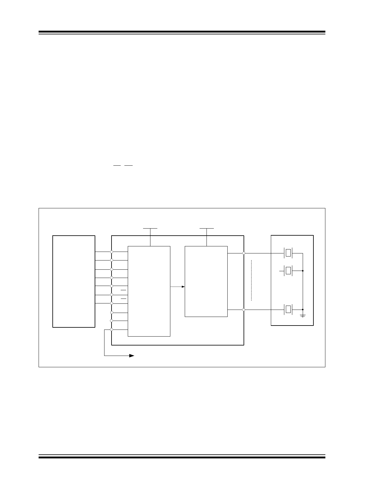
Application Information
HV582 is designed for applications requiring multiple
high-voltage outputs with current sinking and sourcing
capabilities in the range of
±
75 mA. Typical
applications where the HV582 is utilized are in plasma
displays, Inkjet printer drivers and 3D printer drivers.
FIGURE 3-1:
Typical Application Block Diagram.
Low Voltage
Shift Register
Latches
Output Control
High Voltage
Level Translators
and
Push-Pull Output
Buffers
Microprocessor
D (1-6) A
CLK
POL
LE
OE
OL
OH
DIR
Piezo Element
High-Voltage
Power Supply
Low-Voltage
Power Supply
HV582
HV
OUT
1
HV
OUT
96
D
IN(1-6)
for Cascading the next HV582
RST
D (1-6) B