
2016 Microchip Technology Inc.
DS20005629A-page 1
HV5812
Features
• HVCMOS
®
Technology for High Performance
• Operating Voltage of up to 80V
• High-speed Source Driver
• 5V CMOS Logic Circuitry
• Up to 5 MHz Data Input Rate
• Excellent Noise Immunity
• Flexible High-voltage Supplies
Applications
• Display Driver
General Description
The HV5812 is a 20-channel serial-input vacuum
fluorescent display driver. It combines a 20-bit CMOS
shift register, data latches and control circuitry with
high-voltage MOSFET outputs. The HV5812 is
primarily designed for vacuum fluorescent displays.
The CMOS shift register and latches allow direct
interfacing with microprocessor-based systems. Data
input rates are typically over 5 MHz with 5V logic
supply. Especially useful for interdigit blanking, the
blanking input disables the output source drives and
turns on the sink drivers. Using with TTL may require
external pull-up resistors to ensure an input logic high.
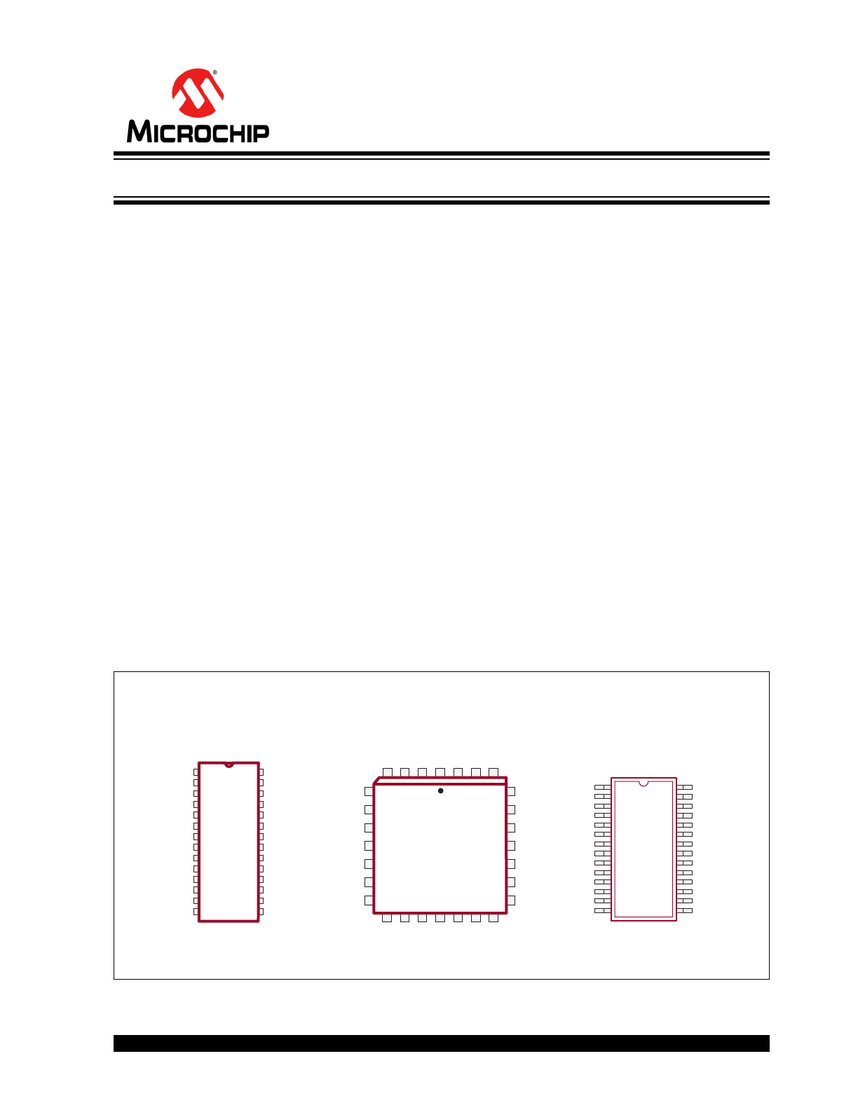
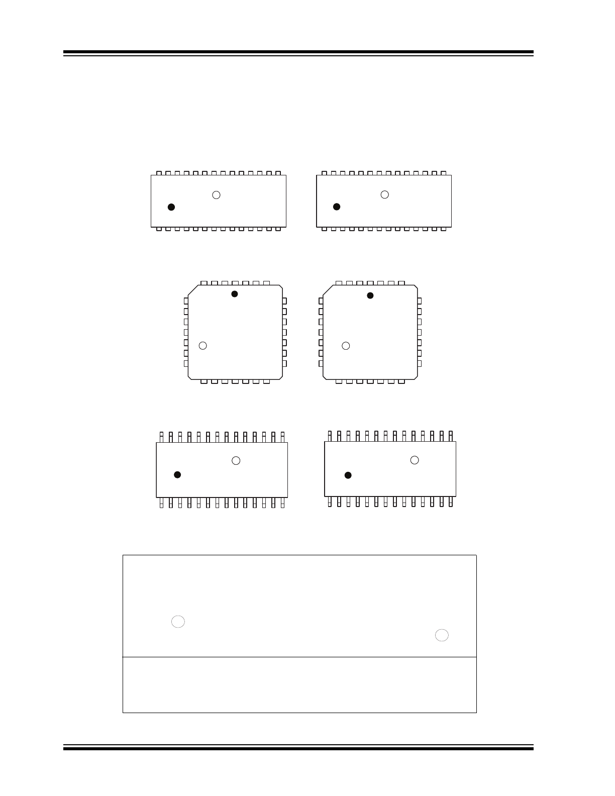
Package Type
28-lead PDIP
(Top view)
See
Table 2-1
for pin information.
28
1
1 28
4
26
1
28
28-lead PLCC
(Top view)
28-lead SOW
(Top view)
s
20-Channel Serial-Input Vacuum Fluorescent Display Driver for Anode or Grid
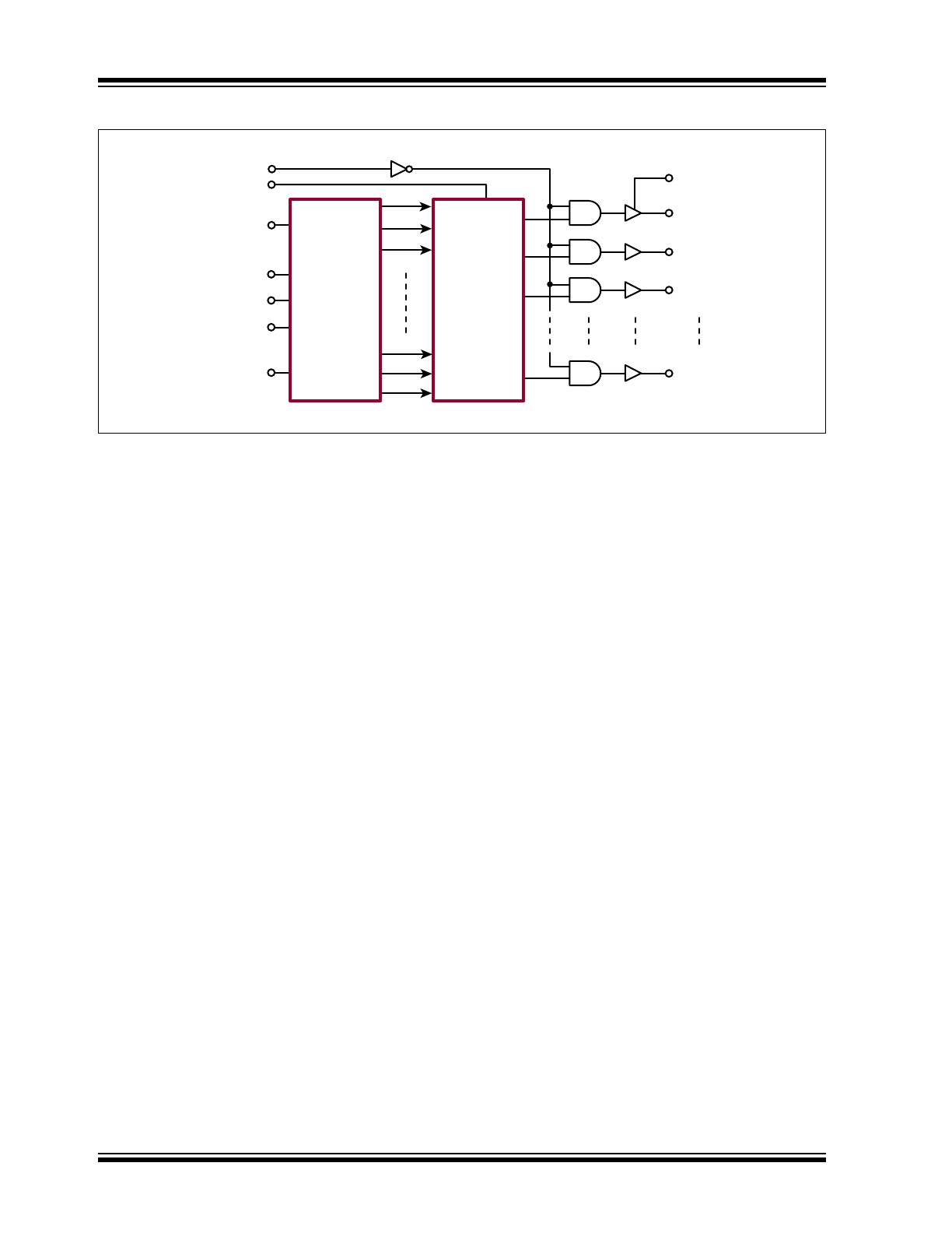
BL
STROBE
DATA IN
CLK
DATA OUT
20-bit
Shift
Register
20-bit
Latch
VPP
HV
OUT
1
HV
OUT
2
HV
OUT
3
HV
OUT
20
GND
VDD
HV5812
DS20005629A-page 2
2016 Microchip Technology Inc.
Functional Block Diagram
2016 Microchip Technology Inc.
DS20005629A-page 3
HV5812
1.0
ELECTRICAL CHARACTERISTICS
Absolute Maximum Ratings†
Supply Voltage, V
DD
................................................................................................................................ –0.5V to +7.5V
Supply Voltage, V
PP
..................................................................................................................................–0.5V to +90V
Logic Input Levels ............................................................................................................................ –0.3V to V
DD
+0.3V
Maximum Operating Junction Temperature .........................................................................................................+125°C
Storage Temperature ............................................................................................................................–55°C to +150°C
Power Dissipation:
28-lead PDIP ......................................................................................................................................... 2000 mW
28-lead PLCC........................................................................................................................................ 1900 mW
28-Lead SOW........................................................................................................................................ 1700 mW
† Notice: Stresses above those listed under “Absolute Maximum Ratings” may cause permanent damage to the
device. This is a stress rating only, and functional operation of the device at those or any other conditions above those
indicated in the operational sections of this specification is not intended. Exposure to maximum rating conditions for
extended periods may affect device reliability.
RECOMMENDED OPERATING CONDITIONS
Parameter
Sym.
Min.
Typ.
Max.
Unit
Conditions
Supply Voltage
V
DD
4.5
—
5.5
V
Supply Voltage
V
PP
20
—
80
V
Operating Junction Temperature
T
J
–40
—
+125
°C
DC ELECTRICAL CHARACTERISTICS
Electrical Specifications: Over recommended operating conditions; T
A
= 25°C unless otherwise indicated.
Parameter
Sym.
Min.
Typ.
Max.
Unit
Conditions
Output Leakage Current
I
DSS
—
–5
–15
µA
V
OUT
= 0V, T
A
= +70°C
High-level Output
V
OH
HV
OUT
78
78.5
—
V
I
OUT
= –25 mA, V
PP
= 80V,
T
J
= +25°C
77
78
—
I
OUT
= –25 mA, V
PP
= 80V,
T
J
= +125°C
DATA
OUT
4.5
4.7
—
V
I
OUT
= –200 µA, V
DD
= 5V
Low-level Output
V
OL
HV
OUT
—
1.5
3
V
I
OUT
= 1 mA, T
J
= +25°C, V
DD
= 5V
—
2.3
4
I
OUT
= 1 mA, T
J
= +125°C,
V
DD
= 5V
DATA
OUT
—
200
250
V
I
OUT
= +200 µA, V
DD
= 5V
Output Pull-down Current
I
SINK
2
3.5
—
mA
V
OUT
= 5V to V
PP
, V
DD
= 5V
High-level Logic Input Voltage
V
IH
3.5
—
5.3
V
V
DD
= 5V
Low-level Logic Input Voltage
V
IL
–0.3
—
0.8
V
High-level Logic Input Current
I
IH
—
0.05
0.5
µA
V
IN
= V
DD
, V
DD
= 5V
Low-level Logic Input Current
I
IL
—
–0.05
–0.5
µA
V
IN
= 0.8V, V
DD
= 5V
Quiescent V
DD
Supply
Current
I
DDQ
—
100
300
µA
All outputs high, V
DD
= 5V
—
100
300
All outputs low, V
DD
= 5V
Quiescent V
PP
Supply Current
I
PPQ
—
10
100
µA
All outputs high, no load
—
10
100
All outputs low, no load
AC ELECTRICAL CHARACTERISTICS
Electrical Specifications: Over recommended operating conditions; T
A
= 25°C unless otherwise indicated.
Parameter
Sym.
Min.
Typ.
Max.
Unit
Conditions
Blanking to Output Delay
t
PHL
—
2000
—
ns
C
L
= 30 pF, 50% to 50%, V
DD
=5V
t
PLH
—
1000
—
Output Fall Time
t
r
—
1450
—
ns
C
L
= 30 pF, 90% to 10%, V
DD
= 5V
Output Rise Time
t
f
—
650
—
ns
C
L
= 30 pF, 10% to 90%, V
DD
= 5V
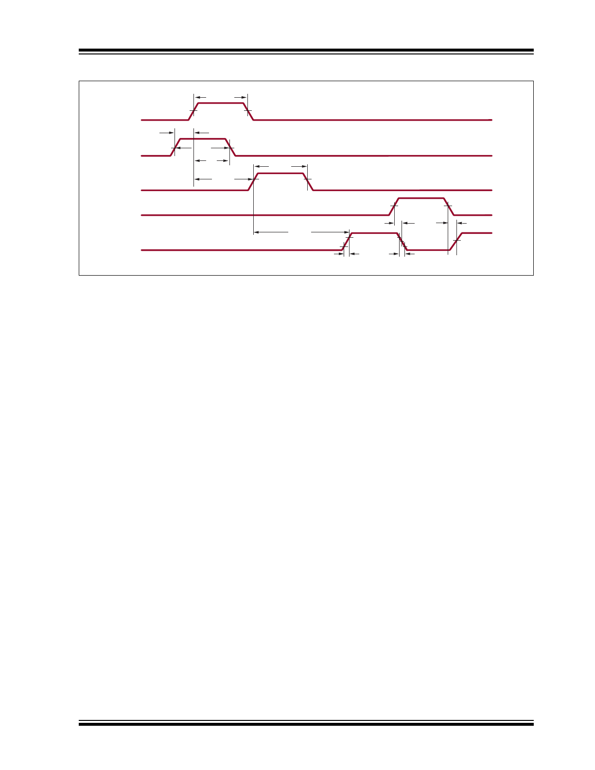
Data Set-up Time
t
SU
75
—
—
ns
See
Timing Waveforms
.
Data Hold Time
t
H
75
—
—
ns
See
Timing Waveforms
.
Minimum Data Pulse Width
t
PWD
150
—
—
ns
See
Timing Waveforms
.
Minimum Clock Pulse Width
t
PWCLK
150
—
—
ns
See
Timing Waveforms
.
Minimum Time between Clock
Activation and Strobe
t
CKS
300
—
—
ns
See
Timing Waveforms
.
Minimum Strobe Pulse Width
t
PWS
100
—
—
ns
See
Timing Waveforms
.
Typical Time between Strobe
Activation and Output
Transition
t
STO
—
500
—
ns
See
Timing Waveforms
.
Maximum Clock Frequency
f
CLK
—
8
—
MHz
T
J
= +25°C, V
DD
= 5V
—
5
—
T
J
= +125°C, V
DD
= 5V
TEMPERATURE SPECIFICATIONS
Parameter
Sym.
Min.
Typ.
Max.
Unit
Conditions
TEMPERATURE RANGE
Operating Junction Temperature
T
J
–40
—
+125
°C
Storage Temperature
T
S
–55
—
+150
°C
PACKAGE THERMAL RESISTANCE
28-lead PDIP
JA
—
43
—
°C/W
28-lead PLCC
JA
—
48
—
°C/W
28-lead SOW
JA
—
55
—
°C/W
HV5812
DS20005629A-page 4
2016 Microchip Technology Inc.
2016 Microchip Technology Inc.
DS20005629A-page 5
HV5812
Timing Waveforms
CLK
DATA IN
STROBE
BL
HV
OUT
t
PWCLK
t
PWS
t
PHL
t
f
t
r
t
PLH
t
SU
50%
90%
10%
50%
10%
t
h
t
PWD
t
CKS
t
STO
90%
50%
50%
50%
50%
50%
50%
V
IH
V
IL
V
IH
V
IL
V
IH
V
IL
V
IH
V
IL
V
OH
V
OL
50%
50%

HV5812
DS20005629A-page 6
2016 Microchip Technology Inc.
2.0
PIN DESCRIPTION
The details on the pins of HV5812 28-lead PDIP,
28-lead PLCC and 28-lead SOW are listed on
Table 2-1
. Refer to
Package Types
for the location of
pins.
TABLE 2-1:
PIN FUNCTION TABLE
Pin Number
Pin Name
Description
1
VPP
High-voltage power rail
2
Data Out
Serial data output. Data output for cascading to the data input of the next device.
3
HV
OUT
20
High-voltage output
4
HV
OUT
19
High-voltage output
5
HV
OUT
18
High-voltage output
6
HV
OUT
17
High-voltage output
7
HV
OUT
16
High-voltage output
8
HV
OUT
15
High-voltage output
9
HV
OUT
14
High-voltage output
10
HV
OUT
13
High-voltage output
11
HV
OUT
12
High-voltage output
12
HV
OUT
11
High-voltage output
13
BLANKING
Blank
14
GND
Logic and high-voltage ground
15
CLOCK
Data shift register clock
16
STROBE
Strobe
17
HV
OUT
10
High-voltage output
18
HV
OUT
9
High-voltage output
19
HV
OUT
8
High-voltage output
20
HV
OUT
7
High-voltage output
21
HV
OUT
6
High-voltage output
22
HV
OUT
5
High-voltage output
23
HV
OUT
4
High-voltage output
24
HV
OUT
3
High-voltage output
25
HV
OUT
2
High-voltage output
26
HV
OUT
1
High-voltage output
27
Data In
Serial data input
28
VDD
Low-voltage logic power rail
2016 Microchip Technology Inc.
DS20005629A-page 7
HV5812
3.0
FUNCTIONAL DESCRIPTION
Follow the steps below to power up and power down
the HV5812:
POWER-UP AND POWER-DOWN SEQUENCE
Power-up
Power-down
Step
Description
Step
Description
1
Connect ground.
1
Remove V
PP
.
2
Apply V
DD
.
2
Remove all inputs.
3
Set all inputs (Data, CLK, etc.) to a known state
3
Remove V
DD
.
4
Apply V
PP
. (
Note 1
)
4
Disconnect ground.
Note 1: The V
PP
should not drop below V
DD
during operation.
FUNCTION TABLE (
Note 1
)
Serial
Data
Input
Clock
Input
Shift Register Contents
Serial
Data
Output
Strobe
Input
Latch Contents
Blanking
Output Contents
I
1
I
2
I
3
... I
N-1
I
N
I
1
I
2
I
3
... I
N-1
I
N
I
1
I
2
I
3
... I
N-1
I
N
H
L to H
H
R
1
R
2
...R
N–2
R
N–1
R
N–1
—
—
—
—
—
—
—
—
—
—
L
L to H
L
R
1
R
2
...R
N–2
R
N–1
R
N–1
—
—
—
—
—
—
—
—
—
—
X
H to L R
1
R
2
R
3
...R
N–1
R
N
R
N
—
—
—
—
—
—
—
—
—
—
—
—
X
X
X...X
X
X
L
R
1
R
2
R
3
...R
N–1
R
N
—
—
—
—
—
—
—
P
1
P
2
P
3
...P
N–1
P
N
P
N
H
P
1
P
2
P
3
...P
N–1
P
N
L
P
1
P
2
P
3
...P
N–1
P
N
—
—
—
—
—
—
—
—
X
X
X...X
X
H
L
L
L...L
L
Note 1:
L = Low logic level
H = High logic level
X = Irrelevant
P = Present state
R = Previous state
,
VDD
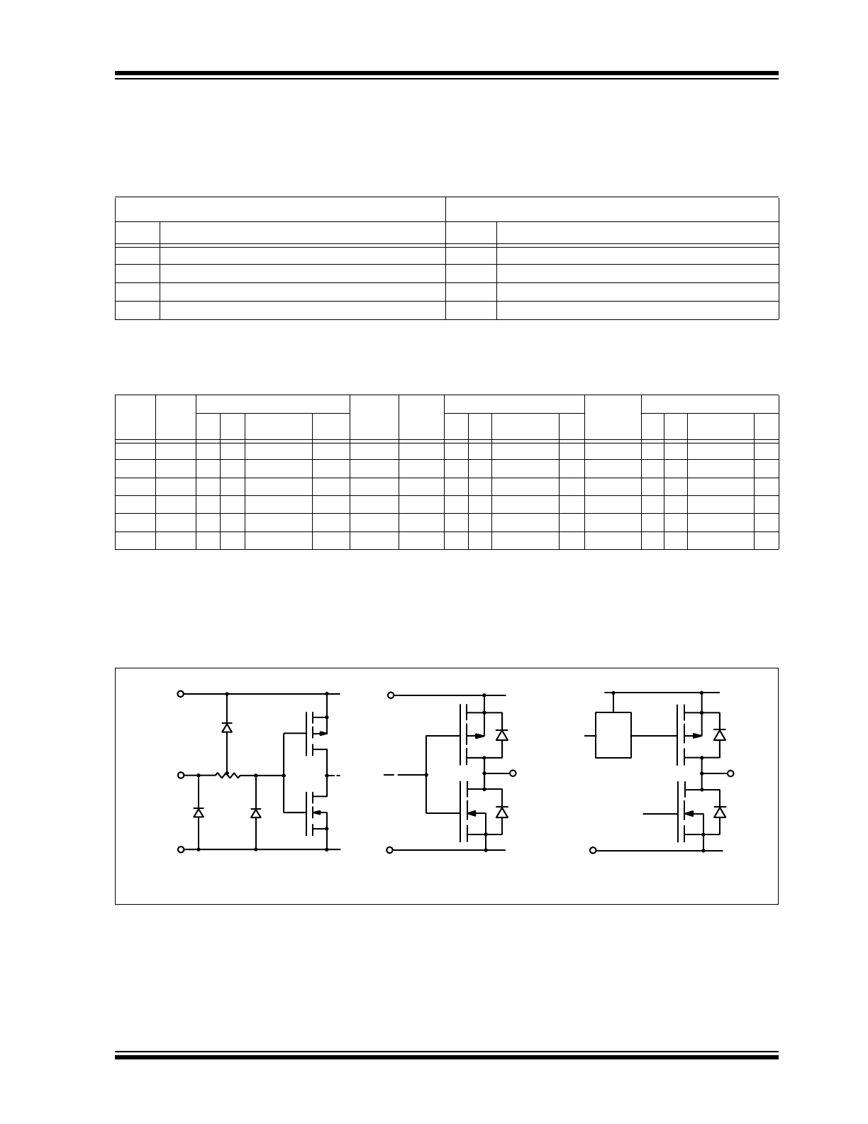
INPUT
GND
VPP
L/T
GND
HV
OUT
Logic Inputs
GND
Data Out
Logic Data Output
High Voltage Outputs
VDD
FIGURE 3-1:
IO Circuits.
HV5812
DS20005629A-page 8
2016 Microchip Technology Inc.
4.0
PACKAGE MARKING INFORMATION
4.1
Packaging Information
28-lead PDIP
Example
HV5812P
e3
1625859
XXXXXX
e3
YYWWNNN
Legend: XX...X
Product Code or Customer-specific information
Y
Year code (last digit of calendar year)
YY
Year code (last 2 digits of calendar year)
WW
Week code (week of January 1 is week ‘01’)
NNN
Alphanumeric traceability code
Pb-free JEDEC
®
designator for Matte Tin (Sn)
*
This package is Pb-free. The Pb-free JEDEC designator ( )
can be found on the outer packaging for this package.
Note:
In the event the full Microchip part number cannot be marked on one line, it will
be carried over to the next line, thus limiting the number of available
characters for product code or customer-specific information. Package may or
not include the corporate logo.
3
e
3
e
XXXXXXX
e3
YYWWNNN
e3
HV5812WG
1678896
28-lead SOW
Example
28-lead PLCC
Example
XXXXXXXXX
YYWWNNN
e3
HV5812PJ
1611231
e3
28-Lead PDIP (.600in Row Spacing) Package Outline (P)
1.565x.580in body, .250in height (max), .100in pitch
Note 1
(Index Area)
28
1
D
L
A1
A
A2
Seating
Plane
e
E1
D1
D1
E
A
A
Side View
Top View
View A - A
eA
eB
b
b1
View B
View B
Note:
1.
$3LQLGHQWL¿HUPXVWEHORFDWHGLQWKHLQGH[DUHDLQGLFDWHG7KH3LQLGHQWL¿HUFDQEHDPROGHGPDUNLGHQWL¿HUDQHPEHGGHGPHWDOPDUNHURU
DSULQWHGLQGLFDWRU
Symbol
A
A1
A2
b
b1
D
D1
E
E1
e
eA
eB
L
Dimension
(inches)
MIN
.140*
.015
.125
.014
.030
1.380
.065
†
.590
†
.485
.100
BSC
.600
BSC
.600*
.115
NOM
-
-
-
-
-
-
-
-
-
-
-
MAX
.250
.055*
.195
.023
†
.070
1.565
.085*
.625
.580
.700
.200
-('(&5HJLVWUDWLRQ069DULDWLRQ$%,VVXH%-XQH
7KLVGLPHQVLRQLVQRWVSHFL¿HGLQWKH-('(&GUDZLQJ
7KLVGLPHQVLRQGLIIHUVIURPWKH-('(&GUDZLQJ
Drawings not to scale.
Note: For the most current package drawings, see the Microchip Packaging Specification at www.microchip.com/packaging.
Note: For the most current package drawings, see the Microchip Packaging Specification at www.microchip.com/packaging.
2016 Microchip Technology Inc.
DS20005629A-page 9
HV5812
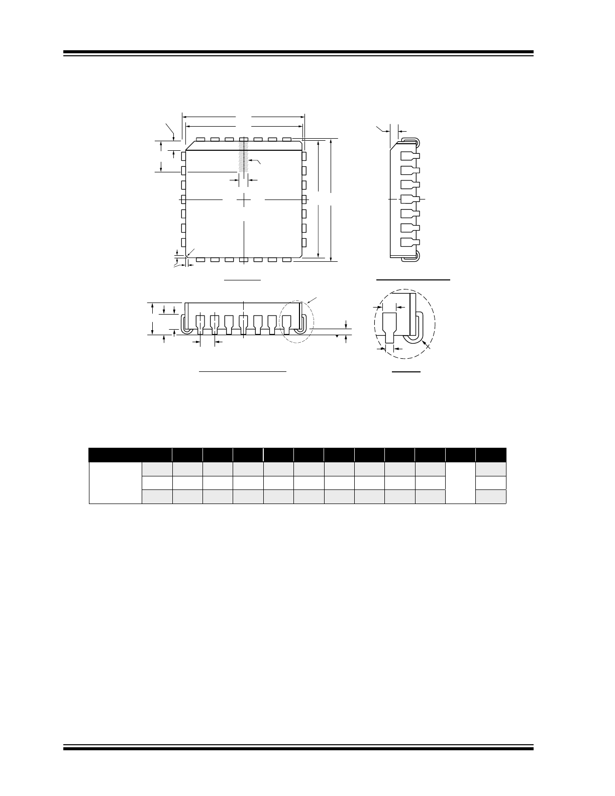
28-Lead PLCC Package Outline (PJ)
.453x.453in. body, .180in. height (max), .050in. pitch
Symbol
A
A1
A2
b
b1
D
D1
E
E1
e
R
Dimension
(inches)
MIN
.165
.090
.062
.013
.026
.485
.450
.485
.450
.050
BSC
.025
NOM
.172
.105
-
-
-
.490
.453
.490
.453
.035
MAX
.180
.120
.083
.021
.032
.495
.456
.495
.456
.045
JEDEC Registration MS-018, Variation AB, Issue A, June, 1993.
Drawings not to scale.
.150 MAX
.048/.042
x 45
O
1
075 MAX
4
26
D
D1
E1 E
Top View
View A
A
A2
A1
Seating
Plane
e
Note 1
(Index Area)
.056/.042
x 45
O
Base
Plane
.020 MIN
28
b
View A
b1
Horizontal Side View
Vertical Side View
Note 2
.020max
(3 Places)
R
Notes:
1.
$3LQLGHQWL¿HUPXVWEHORFDWHGLQWKHLQGH[DUHDLQGLFDWHG7KH3LQLGHQWL¿HUFDQEHDPROGHGPDUNLGHQWL¿HUDQHPEHGGHGPHWDOPDUNHURU
a printed indicator.
2.
$FWXDOVKDSHRIWKLVIHDWXUHPD\YDU\
Note: For the most current package drawings, see the Microchip Packaging Specification at www.microchip.com/packaging.
Note: For the most current package drawings, see the Microchip Packaging Specification at www.microchip.com/packaging.
HV5812
DS20005629A-page 10
2016 Microchip Technology Inc.