
2017 Microchip Technology Inc.
DS20005699A-page 1
HV5522
Features
• 100 mA Minimum Sink Current
• 8 MHz Shift Register Speed
• Polarity and Blanking Inputs
• CMOS-compatible Inputs
• Forward and Reverse Shifting Options
• Diode to V
PP
allows Efficient Power Recovery
Applications
• Inkjet and Electrostatic Print Heads
• AC-electroluminescent Displays
• Microelectromechanical Systems Applications
General Description
The HV5522 is a low-voltage to high-voltage
serial-to-parallel converter with open drain outputs.
This device is designed as a driver for AC
electroluminescent displays. It can also be used in any
application requiring multiple-output high-voltage
current sinking capabilities, such as driving inkjet and
electrostatic print heads, plasma panels, vacuum
fluorescent and large matrix LCD displays.
This device consists of a 32-bit Shift register, 32 latches
and control logic to perform the polarity select and
blanking of the outputs. Data is shifted through the Shift
register on the high-to-low transition of the clock. The
HV5522 shifts the data counter clockwise when viewed
from the top of the package. A data output buffer is
provided for cascading devices. This output reflects the
current status of the last bit of the Shift register. The
operation of the Shift register is not affected by the latch
enable (LE), blanking (BL) and polarity (POL) inputs.
The transfer of data from the Shift register to the latch
occurs when the LE input is high. The data in the latch
is stored when LE is low.
Package Type
See
Table 2-1
and
Table 2-2
for pin information.
44-lead PQFP
(Top view)
1
44
1 44
6
40
44-lead PLCC
(Top view)
s
32-Channel Serial-to-Parallel Converter with Open Drain Outputs
POL
BL
LE
DATA
IN
CLK
DATA
OUT
HV
OUT
1
(Outputs 3 to 30 not shown)
Latch
Latch
HV
OUT
2
HV
OUT
31
HV
OUT
32
Latch
Latch
32-Bit
Shift
Register
HV5522
DS20005699A-page 2
2017 Microchip Technology Inc.
Functional Block Diagram
2017 Microchip Technology Inc.
DS20005699A-page 3
HV5522
Typical Application Circuit
HV5522
DS20005699A-page 4
2017 Microchip Technology Inc.
1.0
ELECTRICAL CHARACTERISTICS
Absolute Maximum Ratings†
Supply Voltage, V
DD
(
Note 1
) .................................................................................................................. –0.5V to +15V
Output Voltage, V
PP
(
Note 1
) ................................................................................................................ –0.5V to +230V
Logic Input Levels (
Note 1
)
.............................................................................................................. –0.5V to V
DD
+0.5V
Ground Current (
Note 2
)
......................................................................................................................................... 1.5A
Operating Ambient Temperature, T
A
..................................................................................................... –40°C to +85°C
Storage Temperature, T
S
...................................................................................................................... –65°C to +150°C
Continuous Total Power Dissipation:
44-lead PQFP (
Note 3
) ......................................................................................................................... 1200 mW
44-lead PLCC (
Note 3
) ......................................................................................................................... 1200 mW
† Notice: Stresses above those listed under “Absolute Maximum Ratings” may cause permanent damage to the
device. This is a stress rating only, and functional operation of the device at those or any other conditions above those
indicated in the operational sections of this specification is not intended. Exposure to maximum rating conditions for
extended periods may affect device reliability.
Note 1:
All voltages are referenced to V
SS
.
2:
Duty cycle is limited by the total power dissipated in the package.
3:
For operations above 25°C ambient, derate linearly to the maximum operating temperature of 20 mW/°C.
RECOMMENDED OPERATING CONDITIONS
Parameter
Sym.
Min.
Typ.
Max.
Unit
Conditions
Logic Supply Voltage
V
DD
10.8
—
13.2
V
High-voltage Output Voltage
HV
OUT
–0.3
—
220
V
High-level Input Voltage
V
IH
V
DD
–2
—
V
DD
V
Low-level Input Voltage
V
IL
0
—
2
V
Clock Frequency
f
CLK
—
—
8
MHz
Operating Ambient Temperature
T
A
–40
—
+85
°C
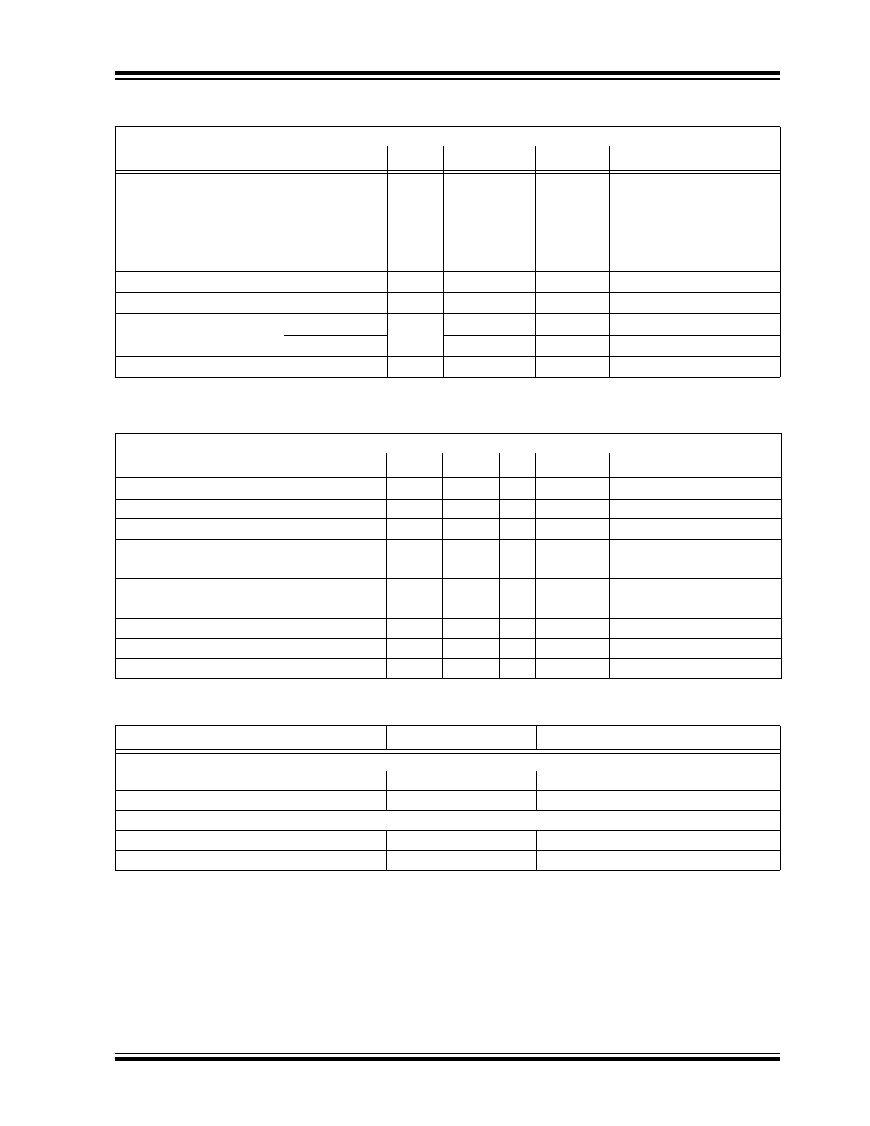
DC ELECTRICAL CHARACTERISTICS
Electrical Specifications: Over recommended operating conditions unless otherwise noted.
Parameter
Sym.
Min.
Typ. Max. Unit
Conditions
V
DD
Supply Current
I
DD
—
—
15
mA f
CLK
= 8 MHz, f
DATA
= 4 MHz
Quiescent V
DD
Supply Current
I
DDQ
—
—
100
µA V
IN
= 0V
Off State Output Current
I
O(OFF)
—
—
10
µA
All outputs high, all SWS
parallel
High-level Logic Input Current
I
IH
—
—
1
µA V
IH
= V
DD
Low-level Logic Input Current
I
IL
—
—
–1
µA V
IL
= 0V
High-level Output Data Out
V
OH
V
DD
–1V
—
—
V
I
DOUT
= –100 µA
Low-level Output
Voltage
HV
OUT
V
OL
—
—
15
V
I
HVOUT
= 100 mA
Data Out
—
—
1
V
I
DOUT
= 100 µA
HV
OUT
Clamp Voltage
V
OC
—
—
–1.5
V
I
OL
= –100 mA
AC ELECTRICAL CHARACTERISTICS
Electrical Specifications: V
DD
= 12V, T
A
= 25°C
Parameter
Sym.
Min.
Typ. Max. Unit
Conditions
Clock Frequency
f
CLK
—
—
8
MHz
Clock Width, High or Low
t
WL
, t
WH
62
—
—
ns
Data Set-up Time before Clock Falls
t
SU
25
—
—
ns
Data Hold Time after Clock Falls
t
H
10
—
—
ns
Turn-on Time, HV
OUT
from Enable
t
ON
—
—
500
ns
R
L
= 2 kΩ to V
PP
maximum
Delay Time Clock to Data High to Low
t
DHL
—
—
100
ns
C
L
= 15 pF
Delay Time Clock to Data Low to High
t
DLH
—
—
100
ns
C
L
= 15 pF
Delay Time Clock to Latch Enable Low to High
t
DLE
50
—
—
ns
Latch Enable Pulse Width
t
WLE
50
—
—
ns
Latch Enable Setup Time before Clock Falls
t
SLE
50
—
—
ns
TEMPERATURE SPECIFICATIONS
Parameter
Sym.
Min.
Typ. Max. Unit
Conditions
TEMPERATURE RANGE
Operating Ambient Temperature
T
A
–40
—
+85
°C
Storage Temperature
T
S
–65
—
+150
°C
PACKAGE THERMAL RESISTANCE
44-lead PQFP
JA
—
51
—
°C/W
44-lead PLCC
JA
—
37
—
°C/W
2017 Microchip Technology Inc.
DS20005699A-page 5
HV5522
HV5522
DS20005699A-page 6
2017 Microchip Technology Inc.
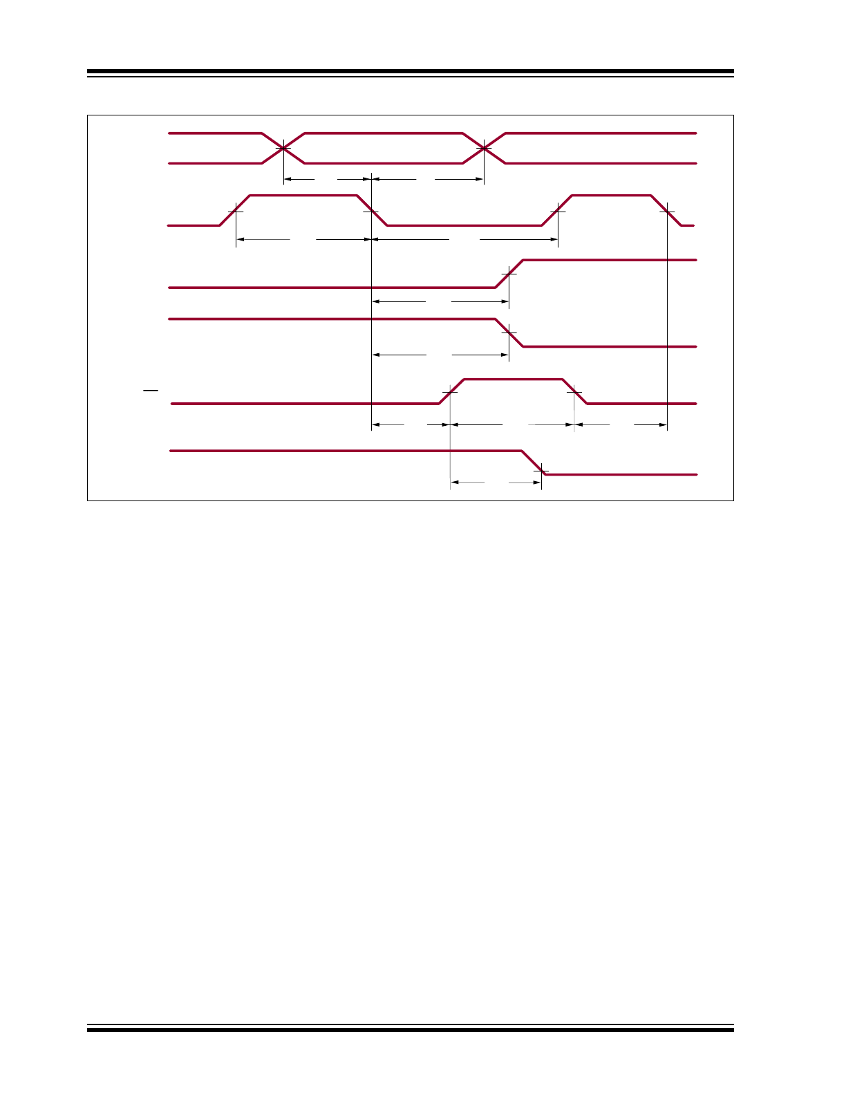
Timing Waveforms
LE
HV
OUT
w/ S/R HIGH
Data Valid
50% 50%
DATA
IN
CLK
DATA
OUT
50% 50% 50%
t
SU
t
H
t
WH
t
WL
50%
50%
t
DLH
t
DHL
50%
t
WLE
t
DLE
t
SLE
50%
50%
10%
t
ON
V
IH
V
IL
V
IH
V
IL
V
OH
V
OL
V
OH
V
OL
V
IH
V
IL
V
OH
V
OL
2017 Microchip Technology Inc.
DS20005699A-page 7
HV5522
2.0
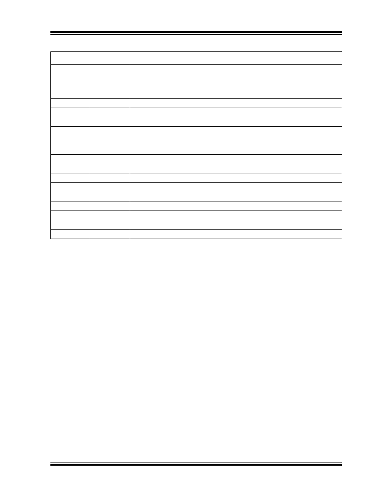
PIN DESCRIPTION
The details on the pins of HV5522 44-lead PQFP and
44-lead PLCC are listed on
Table 2-1
and
Table 2-2
,
respectively. Refer to
Package Types
for the location
of pins.
TABLE 2-1:
44-LEAD PQFP PIN FUNCTION TABLE
Pin Number
Pin Name
Description
1
HVOUT11
High-voltage output
2
HVOUT12
High-voltage output
3
HVOUT13
High-voltage output
4
HVOUT14
High-voltage output
5
HVOUT15
High-voltage output
6
HVOUT16
High-voltage output
7
HVOUT17
High-voltage output
8
HVOUT18
High-voltage output
9
HVOUT19
High-voltage output
10
HVOUT20
High-voltage output
11
HVOUT21
High-voltage output
12
HVOUT22
High-voltage output
13
HVOUT23
High-voltage output
14
HVOUT24
High-voltage output
15
HVOUT25
High-voltage output
16
HVOUT26
High-voltage output
17
HVOUT27
High-voltage output
18
HVOUT28
High-voltage output
19
HVOUT29
High-voltage output
20
HVOUT30
High-voltage output
21
HVOUT31
High-voltage output
22
HVOUT32
High-voltage output
23
DATA OUT
Data output pin
24
NC
No connection
25
NC
No connection
26
NC
No connection
27
POL
Inverts the polarity of the HVOUT pins
28
CLK
Clock pin. Shift registers shift data on the falling edge of input clock.
29
VSS
Reference voltage (usually ground)
30
VDD
Logic supply voltage
31
LE
Latch enable pin. Data is shifted from the Shift register to the latches on logic input
high.
32
DATA IN
Data input pin
33
BL
This blanking pin sets all HVOUT pins low or high, depending on the state of polarity.
See
Table 3-2
.
34
NC
No connection
HV5522
DS20005699A-page 8
2017 Microchip Technology Inc.
35
HVOUT1
High-voltage output
36
HVOUT2
High-voltage output
37
HVOUT3
High-voltage output
38
HVOUT4
High-voltage output
39
HVOUT5
High-voltage output
40
HVOUT6
High-voltage output
41
HVOUT7
High-voltage output
42
HVOUT8
High-voltage output
43
HVOUT9
High-voltage output
44
HVOUT10
High-voltage output
TABLE 2-1:
44-LEAD PQFP PIN FUNCTION TABLE (CONTINUED)
Pin Number
Pin Name
Description
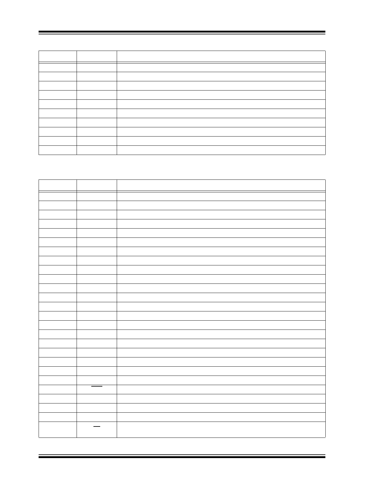
TABLE 2-2:
44-LEAD PLCC PIN FUNCTION TABLE
Pin Number
Pin Name
Description
1
HVOUT16
High-voltage output
2
HVOUT17
High-voltage output
3
HVOUT18
High-voltage output
4
HVOUT19
High-voltage output
5
HVOUT20
High-voltage output
6
HVOUT21
High-voltage output
7
HVOUT22
High-voltage output
8
HVOUT23
High-voltage output
9
HVOUT24
High-voltage output
10
HVOUT25
High-voltage output
11
HVOUT26
High-voltage output
12
HVOUT27
High-voltage output
13
HVOUT28
High-voltage output
14
HVOUT29
High-voltage output
15
HVOUT30
High-voltage output
16
HVOUT31
High-voltage output
17
HVOUT32
High-voltage output
18
DATA OUT
Data output pin
19
NC
No connection
20
NC
No connection
21
NC
No connection
22
POL
Inverts the polarity of the HVOUT pins
23
CLK
Clock pin. Shift registers shift data on the falling edge of the input clock.
24
VSS
Reference voltage (usually ground)
25
VDD
Logic supply voltage
26
LE
Latch enable pin. Data is shifted from the Shift register to the latches on logic input
high.
2017 Microchip Technology Inc.
DS20005699A-page 9
HV5522
27
DATA IN
Data input pin
28
BL
This blanking pin sets all HVOUT pins low or high, depending on the state of polarity.
See
Table 3-2
.
29
NC
No connection
30
HVOUT1
High-voltage output
31
HVOUT2
High-voltage output
32
HVOUT3
High-voltage output
33
HVOUT4
High-voltage output
34
HVOUT5
High-voltage output
35
HVOUT6
High-voltage output
36
HVOUT7
High-voltage output
37
HVOUT8
High-voltage output
38
HVOUT9
High-voltage output
39
HVOUT10
High-voltage output
40
HVOUT11
High-voltage output
41
HVOUT12
High-voltage output
42
HVOUT13
High-voltage output
43
HVOUT14
High-voltage output
44
HVOUT15
High-voltage output
TABLE 2-2:
44-LEAD PLCC PIN FUNCTION TABLE (CONTINUED)
Pin Number
Pin Name
Description
HV5522
DS20005699A-page 10
2017 Microchip Technology Inc.
3.0
FUNCTIONAL DESCRIPTION
Follow the steps in
Table 3-1
to power up and power
down the HV5522.
TABLE 3-1:
POWER-UP AND POWER-DOWN SEQUENCE
Power-up
Power-down
Step
Description
Step
Description
1
Connect ground.
1
Remove all inputs.
2
Apply V
DD
.
2
Remove V
DD
.
3
Set all inputs to a known state.
3
Disconnect ground.
TABLE 3-2:
TRUTH FUNCTION TABLE
Function
Inputs
Outputs
Shift Register
High-voltage Output
Data Out
Data
CLK
LE
BL
POL
1
2
...
32
1
2
...
32
All On
X
X
X
L
L
p1
p2
...
p32
On
On
...
On
d
All Off
X
X
X
L
H
p1
p2
...
p32
Off
Off
...
Off
d
Invert Mode
X
X
L
H
L
p1
p2
...
p32
p1
p2
...
p32
d
Load S/R
H or L
↓
L
H
H
H or L
p1
...
p31
p1
p2
...
p32
p32
Load Latches
X
H or L
↑
H
H
p1
p2
...
p32
p1
p2
...
p32
d
X
H or L
↑
H
L
p1
p2
...
p32
p1
p2
...
p32
d
Transparent
Latch Mode
L
↓
H
H
H
L
p1
...
p31
Off
p1
...
p31
p32
H
↓
H
H
H
H
p1
...
p31
On
p1
...
p31
p32
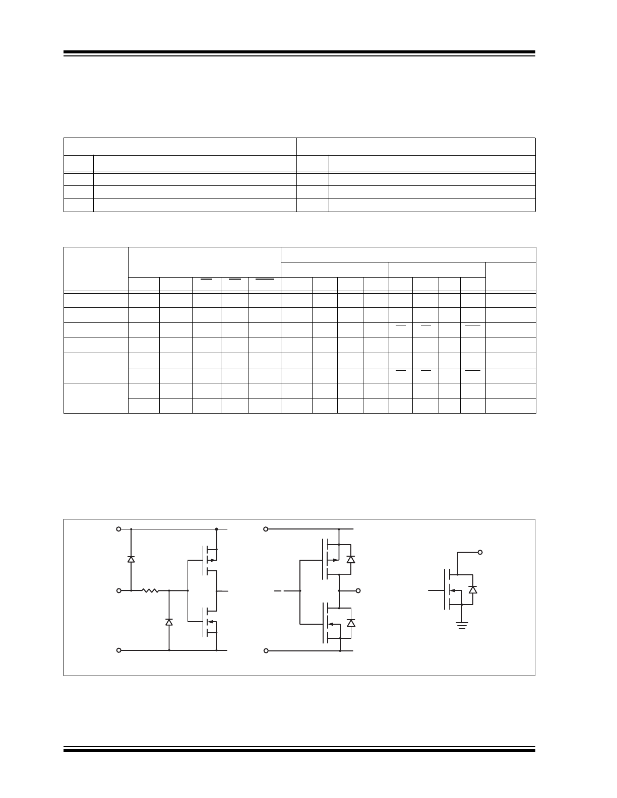
VDD
DATA
IN
HV
OUT
Logic Inputs
DATA
OUT
Logic Data Output
High Voltage Outputs
VDD
HV
IN
VSS
VSS
VSS
Note:
H = High-logic level
L = Low-logic level
X = Irrelevant
↓ = High-to-low transition
↑ = Low-to-high transition
d = Current state of the data output
pn = “p” represents the current state of the Shift register output, and
“n” represents the channel order.
FIGURE 3-1:
Input and Output Equivalent Circuits.