
2017 Microchip Technology Inc.
DS20005847A-page 1
HV518
Features
• Thirty-two Output Lines
• 90V Output Swing
• Active Pull-down
• Latches on all Outputs
• Up to 6 MHz at V
DD
= 5V
• –40°C to +85°C Operation
Applications
• Vacuum Fluorescent Displays
• DC Plasma Displays
General Description
The HV518 is designed for vacuum fluorescent or
DC plasma applications where it can serve as a
segment, digit or matrix display driver. Each device has
32 outputs, 32 latches and a 32-bit cascadable Shift
register.
Serial data enters the Shift register on the low-to-high
transition of the clock input. With latch enable (LE)
high, parallel data is transferred to the output buffers
through a 32-bit latch. When LE is low, the data is
stored in the latch. When strobe (STR) is low, all
outputs are enabled. If the strobe is high, all outputs are
low.
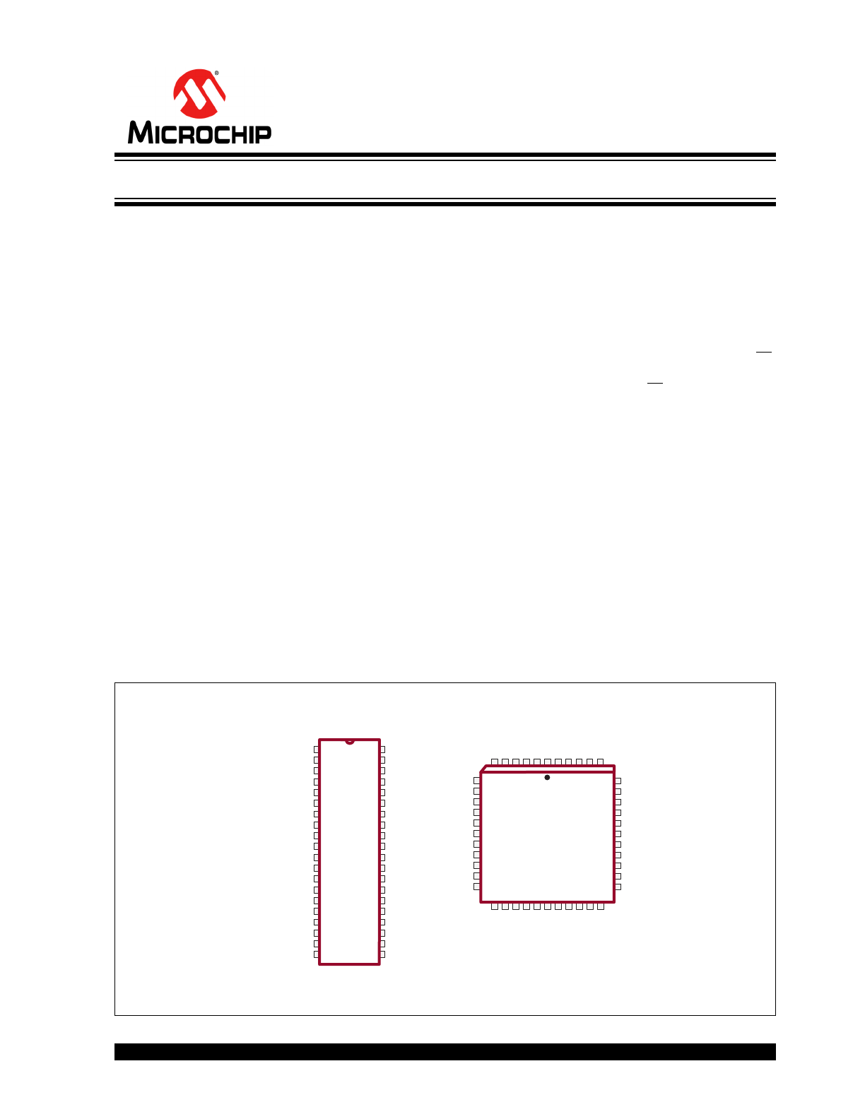
Package Types
See
Table 2-1
and
Table 2-2
for pin information.
40-lead PDIP
(Top view)
44-lead PLCC
(Top view)
40
1
1 44
6
40
32-Channel Vacuum Fluorescent Display Driver
HV518
DS20005847A-page 2
2017 Microchip Technology Inc.
Functional Block Diagram
LE
HV
OUT
1
STR
VPP
DIN
DOUT
CLK
HV
OUT
32
Latches
32-Bit
Shift
Register
2017 Microchip Technology Inc.
DS20005847A-page 3
HV518
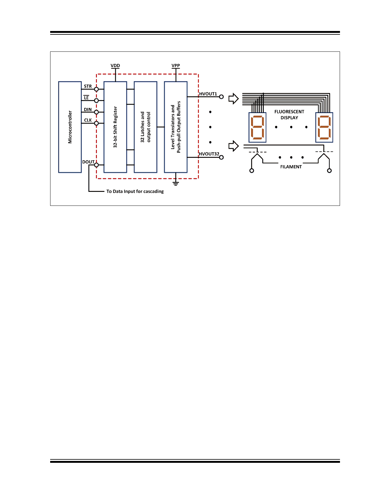
Typical Application Circuit
HV518
DS20005847A-page 4
2017 Microchip Technology Inc.
1.0
ELECTRICAL CHARACTERISTICS
Absolute Maximum Ratings†
Low-voltage Supply Voltage, V
DD
............................................................................................................. –0.5V to +6V
High-voltage Supply Voltage, V
PP
........................................................................................................... –0.5V to +90V
Logic Input Levels ............................................................................................................................. –0.5V to V
DD
+0.5V
Operating Ambient Temperature, T
A
..................................................................................................... –40°C to +85°C
Storage Temperature, T
S
..................................................................................................................... –65°C to +150°C
Continuous Total Power Dissipation:
40-lead PDIP (
Note 1
,
Note 2
) ............................................................................................................. 1200 mW
44-lead PLCC (
Note 1
,
Note 2
) ............................................................................................................ 1200 mW
Note 1: Duty cycle is limited by the total power dissipated in the package.
2: For operations above 25°C ambient, derate linearly to 85°C at 20 mW/°C.
† Notice: Stresses above those listed under “Absolute Maximum Ratings” may cause permanent damage to the
device. This is a stress rating only, and functional operation of the device at those or any other conditions above those
indicated in the operational sections of this specification is not intended. Exposure to maximum rating conditions for
extended periods may affect device reliability.
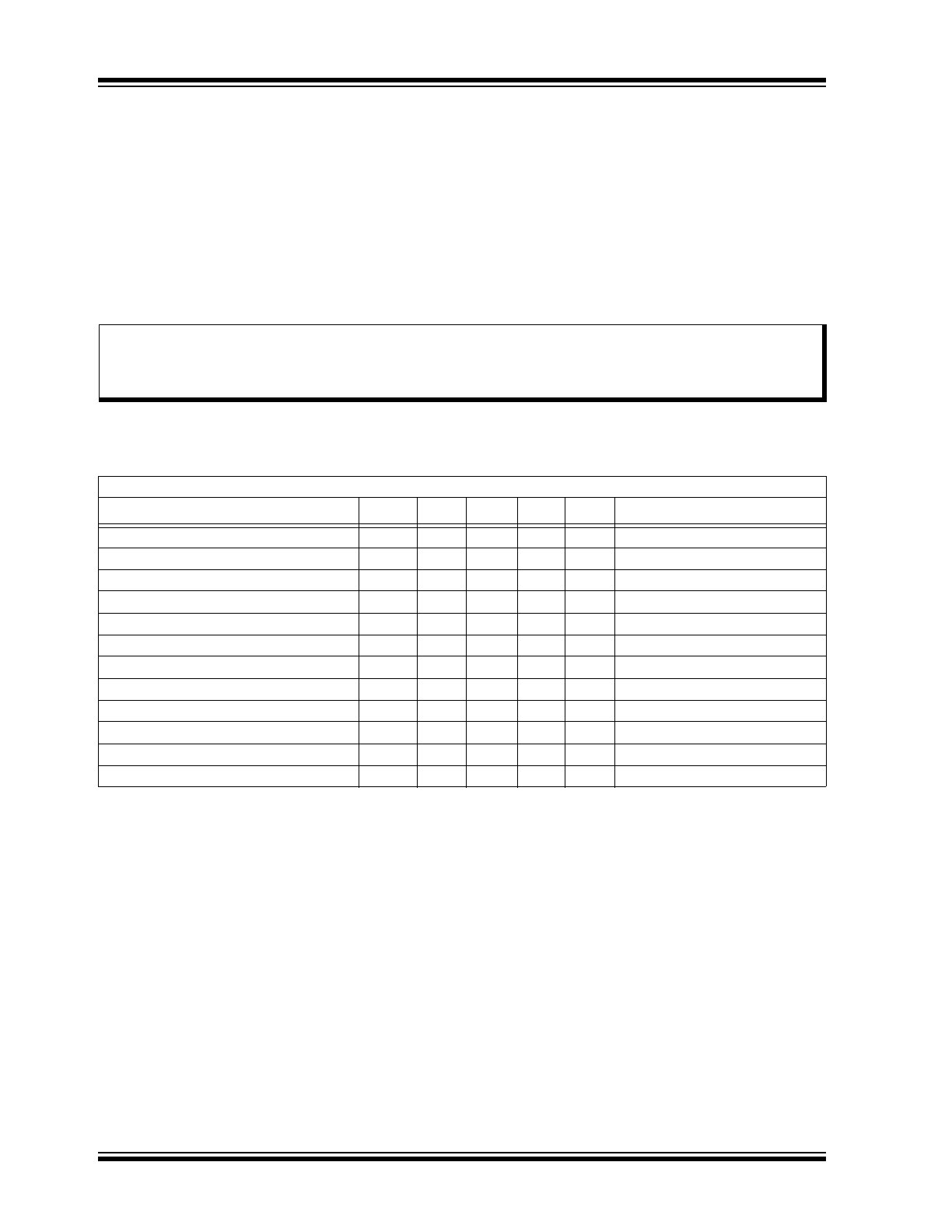
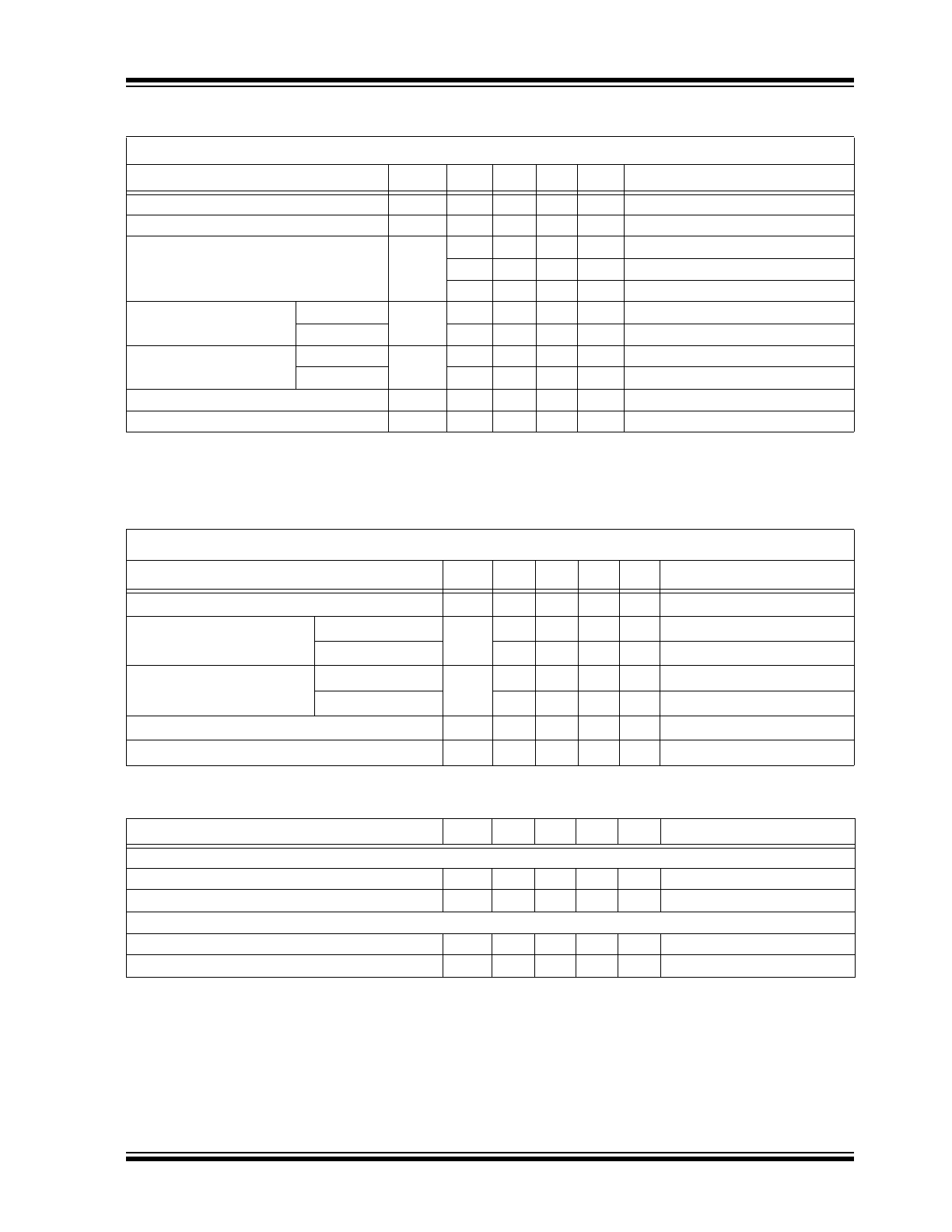
RECOMMENDED OPERATING CONDITIONS
Electrical Specifications: T
A
= 25°C unless otherwise indicated.
Parameter
Sym.
Min.
Typ.
Max.
Unit
Conditions
Logic Supply Voltage
V
DD
4.5
—
5.5
V
High-voltage Supply Voltage
V
PP
8
—
80
V
High-level Input Voltage
V
IH
3.5
—
—
V
V
DD
= 4.5V (See
Figure 3-1
.)
Low-level Input Voltage
V
IL
—
—
1
V
V
DD
= 4.5V (See
Figure 3-1
.)
High-level Output Current
I
OH
–25
—
—
mA
Low-level Output Current
I
OL
—
—
2
mA
Clock Frequency
f
CLK
—
—
6
MHz V
DD
= 4.5V (See
Figure 3-1
.)
Pulse Duration, Clock High
t
W(CKH)
83
—
—
ns
V
DD
= 4.5V
Pulse Duration, Clock Low
t
W(CKL)
83
—
—
ns
V
DD
= 4.5V
Setup Time, Data before Clock
t
SU
75
—
—
ns
V
DD
= 4.5V
Hold Time, Data after Clock
t
H
75
—
—
ns
V
DD
= 4.5V
Operating Ambient Temperature
T
A
–40
—
+85
°C
2017 Microchip Technology Inc.
DS20005847A-page 5
HV518
ELECTRICAL CHARACTERISTICS
Electrical Specifications: Over recommended operating conditions unless otherwise indicated
Parameter
Sym.
Min.
Typ. Max. Unit
Conditions
Supply Current
I
DD
—
—
10
mA
V
DD
= 5V, f
CH
= 6 MHz
Quiescent Supply Current
I
DDQ
—
—
0.5
mA
V
DD
= 5.5V, V
IN
= 0V
Supply Current
I
PP
—
—
12
mA
Outputs high, T
A
= –40°C
—
7
10
mA
Outputs high, T
A
= 0°C to +85°C
—
—
500
µA
Outputs low
HV
IN
Operating Current
HV Output
V
OH
70
—
—
V
I
OH
= –25mA
Serial Output
4.5
4.9
5
V
V
DD
= 5V, I
OH
= –20 µA
LV
IN
Operating Current
HV Output
V
OL
—
—
5
V
I
OL
= 1 mA
Serial Output
—
0.06
0.8
V
I
OL
= 20 µA
Logic Input Current High
I
IH
—
0.1
1
µA
V
IH
= V
DD
Logic Input Current Low
I
IL
—
–0.1
–1
µA
V
IL
= 0V
Note 1: The power dissipation is determined by the number of output at ON state and their duty cycles. The total
power must not exceed the allowable package power dissipation.
SWITCHING CHARACTERISTICS
Electrical Specifications: V
PP
= 80V, C
L
= 50 pF and T
A
= 25°C unless otherwise noted.
Parameter
Sym.
Min. Typ. Max. Unit
Conditions
Delay Time, Clock-to-data Output
t
d
—
—
600
ns
C
L
= 15 pF (See
Figure 3-2
.)
Delay Time, High-to-low
Level, HV Output
From Latch Enable
t
DHL
—
—
1.5
µs
V
DD
= 4.5V (See
Figure 3-3
.)
From Strobe
—
—
1
µs
V
DD
= 4.5V (See
Figure 3-4
.)
Delay Time, Low-to-high
Level, HV Output
From Latch Enable
t
DLH
—
—
1.5
µs
V
DD
= 4.5V (See
Figure 3-3
.)
From Strobe
—
—
1
µs
V
DD
= 4.5V (See
Figure 3-4
.)
Transition Time, High-to-low Level, HV Output
t
THL
—
—
3
µs
V
DD
= 4.5V (See
Figure 3-4
.)
Transition Time, Low-to-high Level, HV Output
t
TLH
—
—
2.5
µs
V
DD
= 4.5V (See
Figure 3-4
.)
TEMPERATURE SPECIFICATIONS
Parameter
Sym. Min. Typ. Max. Unit
Conditions
TEMPERATURE RANGE
Operating Ambient Temperature
T
A
–40
—
+85
°C
Storage Temperature
T
S
–65
—
+150
°C
PACKAGE THERMAL RESISTANCE
40-lead PDIP
JA
—
39
—
°C/W
44-lead PLCC
JA
—
37
—
°C/W
HV518
DS20005847A-page 6
2017 Microchip Technology Inc.
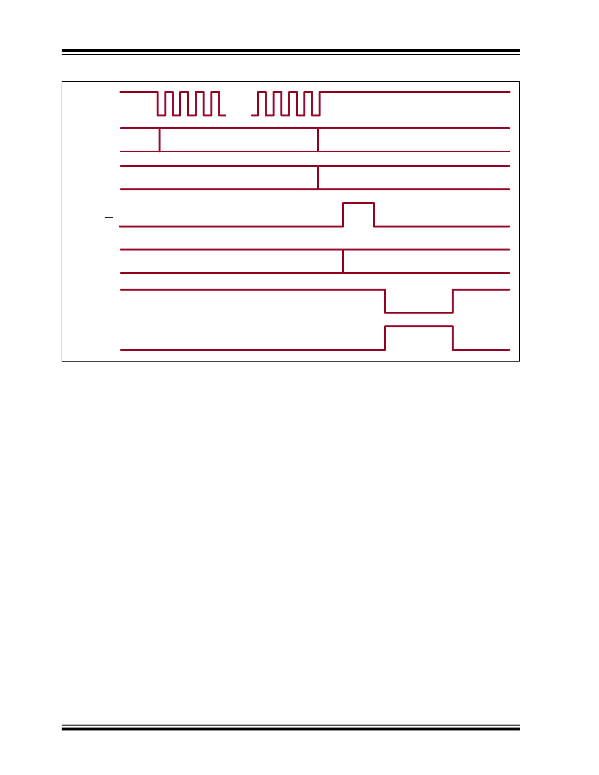
Timing Waveforms
VALID
IRRELEVANT
INVALID VALID
PREVIOUSLY STORED DATA
NEW DATA VALID
VALID
CLK
DATA
IN
SR
CONTENTS
LE
LATCH
CONTENTS
STR
HV
OUTPUT
● ● ●
2017 Microchip Technology Inc.
DS20005847A-page 7
HV518
2.0
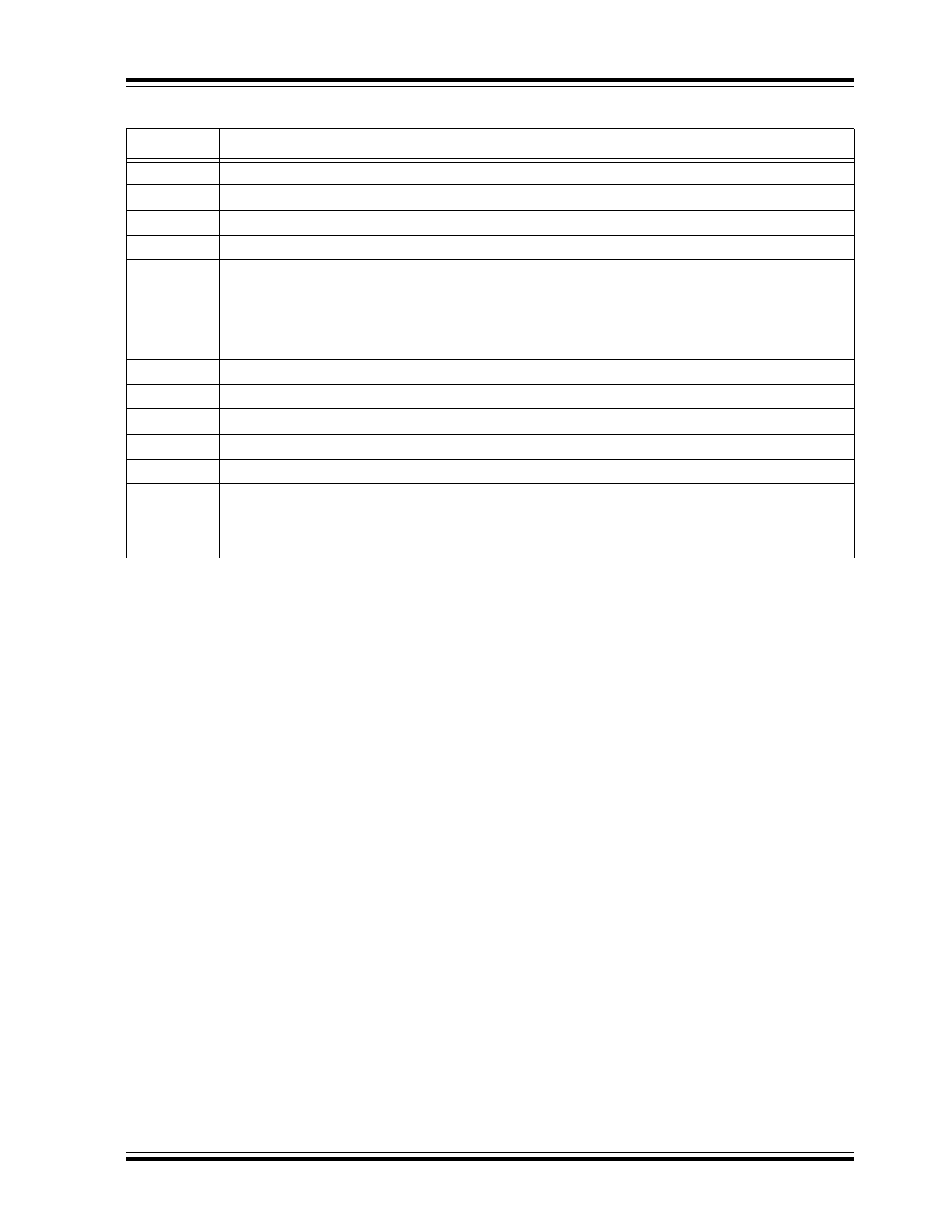
PIN DESCRIPTION
The details on the pins of HV518 40-lead PDIP and
44-lead PLCC are listed on
Table 2-1
and
Table 2-2
,
respectively. Refer to
Package Types
for the location
of pins.
TABLE 2-1:
40-LEAD PDIP PIN FUNCTION TABLE
Pin Number
Pin Name
Description
1
VPP
High-voltage power supply
2
SERIAL OUT
Serial data output
3
HVOUT32
High-voltage output
4
HVOUT31
High-voltage output
5
HVOUT30
High-voltage output
6
HVOUT29
High-voltage output
7
HVOUT28
High-voltage output
8
HVOUT27
High-voltage output
9
HVOUT26
High-voltage output
10
HVOUT25
High-voltage output
11
HVOUT24
High-voltage output
12
HVOUT23
High-voltage output
13
HVOUT22
High-voltage output
14
HVOUT21
High-voltage output
15
HVOUT20
High-voltage output
16
HVOUT19
High-voltage output
17
HVOUT18
High-voltage output
18
HVOUT17
High-voltage output
19
STR
Strobe
20
GND
Ground
21
CLK
Data Shift register clock. Inputs are shifted into the Shift register on the positive
edge of the clock.
22
LE
Latch enable
23
HVOUT16
High-voltage output
24
HVOUT15
High-voltage output
25
HVOUT14
High-voltage output
26
HVOUT13
High-voltage output
27
HVOUT12
High-voltage output
28
HVOUT11
High-voltage output
29
HVOUT10
High-voltage output
30
HVOUT9
High-voltage output
31
HVOUT8
High-voltage output
32
HVOUT7
High-voltage output
33
HVOUT6
High-voltage output
HV518
DS20005847A-page 8
2017 Microchip Technology Inc.
34
HVOUT5
High-voltage output
35
HVOUT4
High-voltage output
36
HVOUT3
High-voltage output
37
HVOUT2
High-voltage output
38
HVOUT1
High-voltage output
39
DATA IN
Serial data input
40
VDD
Low-voltage power supply
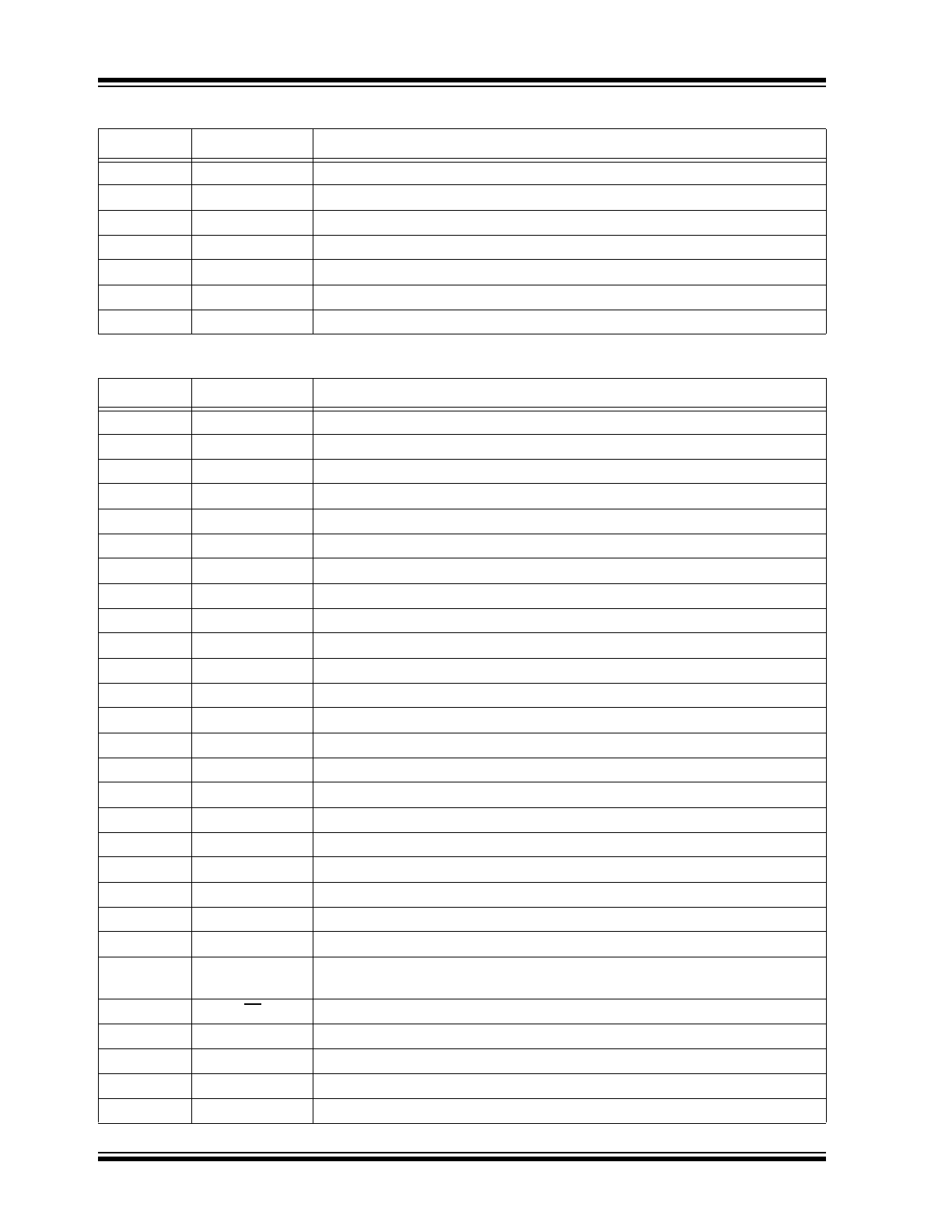
TABLE 2-2:
44-LEAD PLCC PIN FUNCTION TABLE
Pin Number
Pin Name
Description
1
VPP
High-voltage power supply
2
SERIAL OUT
Serial data output
3
HVOUT32
High-voltage output
4
HVOUT31
High-voltage output
5
HVOUT30
High-voltage output
6
NC
No connection
7
HVOUT29
High-voltage output
8
HVOUT28
High-voltage output
9
HVOUT27
High-voltage output
10
HVOUT26
High-voltage output
11
HVOUT25
High-voltage output
12
HVOUT24
High-voltage output
13
HVOUT23
High-voltage output
14
HVOUT22
High-voltage output
15
HVOUT21
High-voltage output
16
HVOUT20
High-voltage output
17
HVOUT19
High-voltage output
18
NC
No connection
19
HVOUT18
High-voltage output
20
HVOUT17
High-voltage output
21
STR
Strobe
22
GND
Ground
23
CLK
Data Shift register clock. Inputs are shifted into the Shift register on the positive
edge of the clock.
24
LE
Latch enable
25
HVOUT16
High-voltage output
26
HVOUT15
High-voltage output
27
HVOUT14
High-voltage output
28
NC
No connection
TABLE 2-1:
40-LEAD PDIP PIN FUNCTION TABLE (CONTINUED)
Pin Number
Pin Name
Description
2017 Microchip Technology Inc.
DS20005847A-page 9
HV518
29
NC
No connection
30
HVOUT13
High-voltage output
31
HVOUT12
High-voltage output
32
HVOUT11
High-voltage output
33
HVOUT10
High-voltage output
34
HVOUT9
High-voltage output
35
HVOUT8
High-voltage output
36
HVOUT7
High-voltage output
37
HVOUT6
High-voltage output
38
HVOUT5
High-voltage output
39
HVOUT4
High-voltage output
40
HVOUT3
High-voltage output
41
HVOUT2
High-voltage output
42
HVOUT1
High-voltage output
43
DATA IN
Serial data input
44
VDD
Low-voltage power supply
TABLE 2-2:
44-LEAD PLCC PIN FUNCTION TABLE (CONTINUED)
Pin Number
Pin Name
Description
HV518
DS20005847A-page 10
2017 Microchip Technology Inc.
3.0
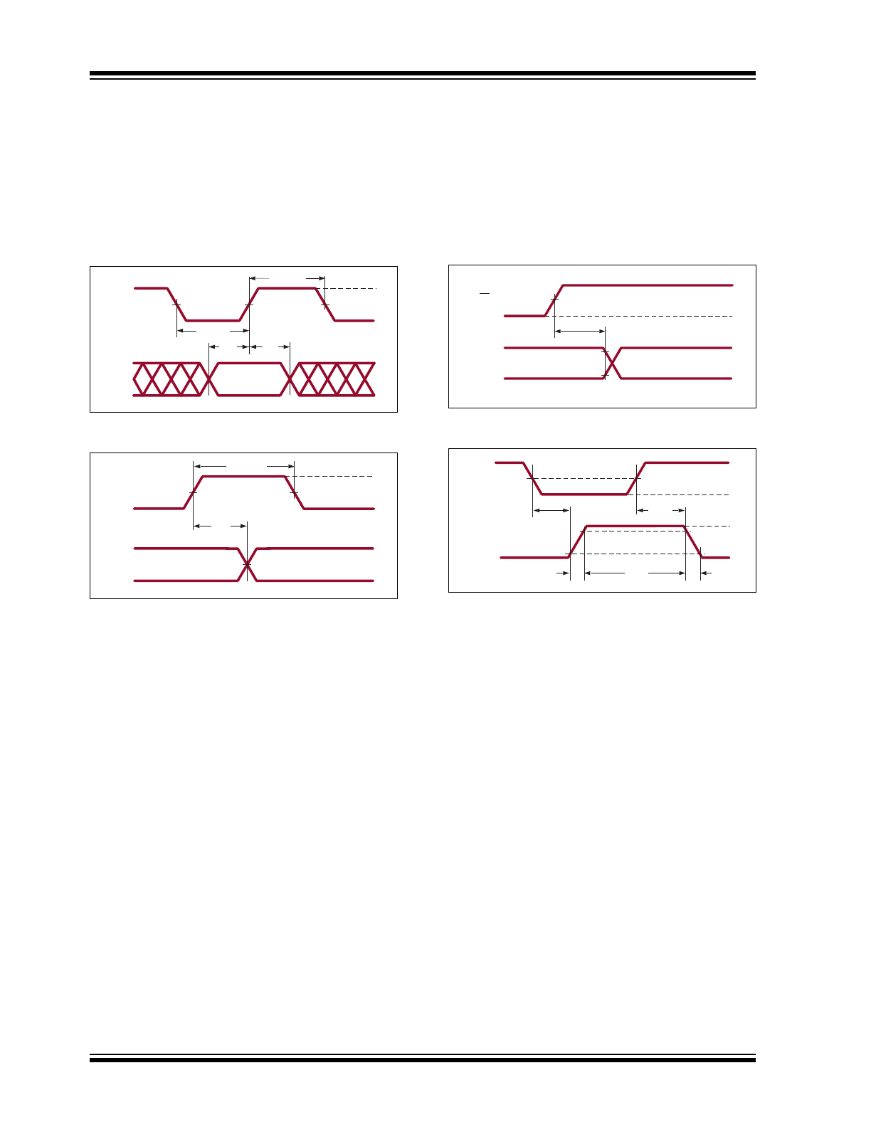
FUNCTIONAL DESCRIPTION
3.1
Parameter Measurement
Information
Figure 3-1
to
Figure 3-4
show parametric
measurement information. For testing purposes, all
input pulses have maximum rise and fall times of
30 nanoseconds.
FIGURE 3-1:
Input Timing Voltage
Waveforms.
FIGURE 3-2:
Output Timing Voltage
Waveforms.
FIGURE 3-3:
Latch Enable Timing
Voltage Waveforms.
FIGURE 3-4:
Switching-Time Voltage
Waveforms.
t
w(CKH)
t
w(CKL)
t
h
t
SU
50%
V
IH
V
IL
V
IH
V
IL
CLK
DATA
IN
t
d
50%
50%
CLK
DATA
OUTPUT
V
IH
V
IL
V
OH
V
OL
t
w(CKH)
50%
90%
t
DLH
or t
DHL
10%
V
OH
V
OL
LE
HV
OUTPUT
V
IH
V
IL
t
THL
90%
10%
t
DLH
t
DHL
V
OH
V
OL
STR
HV
OUTPUT
V
IH
V
IL
50%