
2017 Microchip Technology Inc.
DS20005846A-page 1
HV513
Features
• Up to 250V Output Voltage
• Low-power Level Shifting from 5V to 250V
• Shift Register Speed:
- 8 MHz at V
DD
= 5V
• Latched Data Outputs
• Output Polarity and Blanking
• Output Short-circuit Detect
• Output High-Z (Hi-Z) Control
• CMOS-compatible Inputs
Applications
• Piezoelectric Transducer Driver
• Braille Driver
• Weaving Applications
• Printer Drivers
• Microelectromechanical Systems Applications
• Displays
General Description
The HV513 is a low-voltage to high-voltage
serial-to-parallel converter with eight high-voltage
push-pull outputs. This device is designed to drive
small capacitive loads such as piezoelectric
transducers. It can also be used in any application
requiring multiple high-voltage outputs with
medium-current source-and-sink capabilities.
The device consists of an 8-bit Shift register, eight
latches and control logic to perform the polarity select
and blanking of the outputs. Data is shifted through the
Shift register on the low-to-high transition of the clock.
A data output buffer is provided for cascading devices.
The operation of the Shift register is not affected by the
latch enable (LE), blanking (BL), polarity (POL) and
Hi-Z control inputs. The transfer of data from the Shift
register to the latch occurs when the LE is high. The
data in the latch is stored when LE is low. A Hi-Z pin is
provided to set all the outputs in a High-Z state.
All outputs have short-circuit protection that detects if
the outputs have reached the required output state. If
an output does not track the required state, then the
SHORT pin will be low. This output will pulse low during
the output transition period under normal operation.
See
Figure 3-2
for details.
All outputs will have a break-before-make circuitry to
reduce crossover current during output state changes.
The POL, BL, LE and Hi-Z inputs have an internal
pull-up resistor.
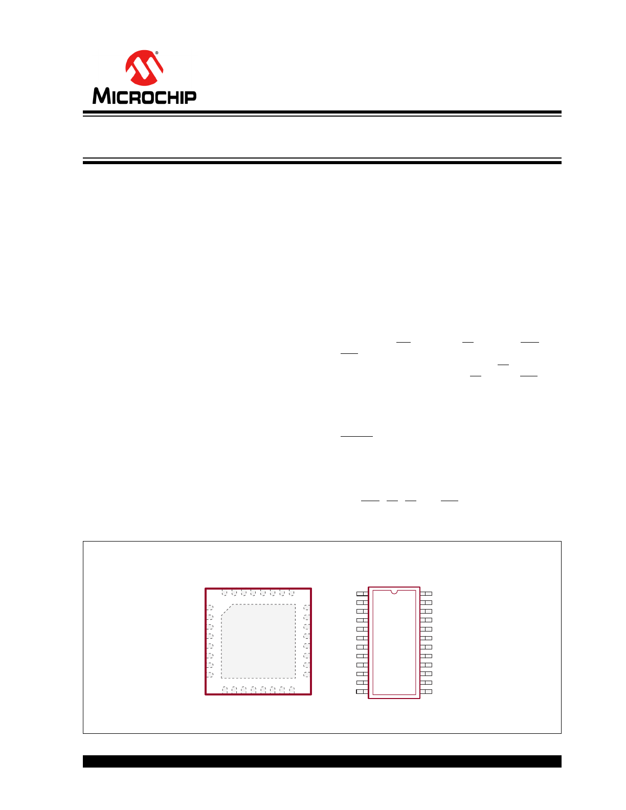
Package Types
1
32
See
Table 2-1
and
Table 2-2
for pin information.
32-lead QFN
(Top view)
24-lead SOW
(Top view)
1
24
8-Channel Serial-to-Parallel Converter with High-Voltage Push-Pull Outputs,
Polarity, Hi-Z and Short-Circuit Detect
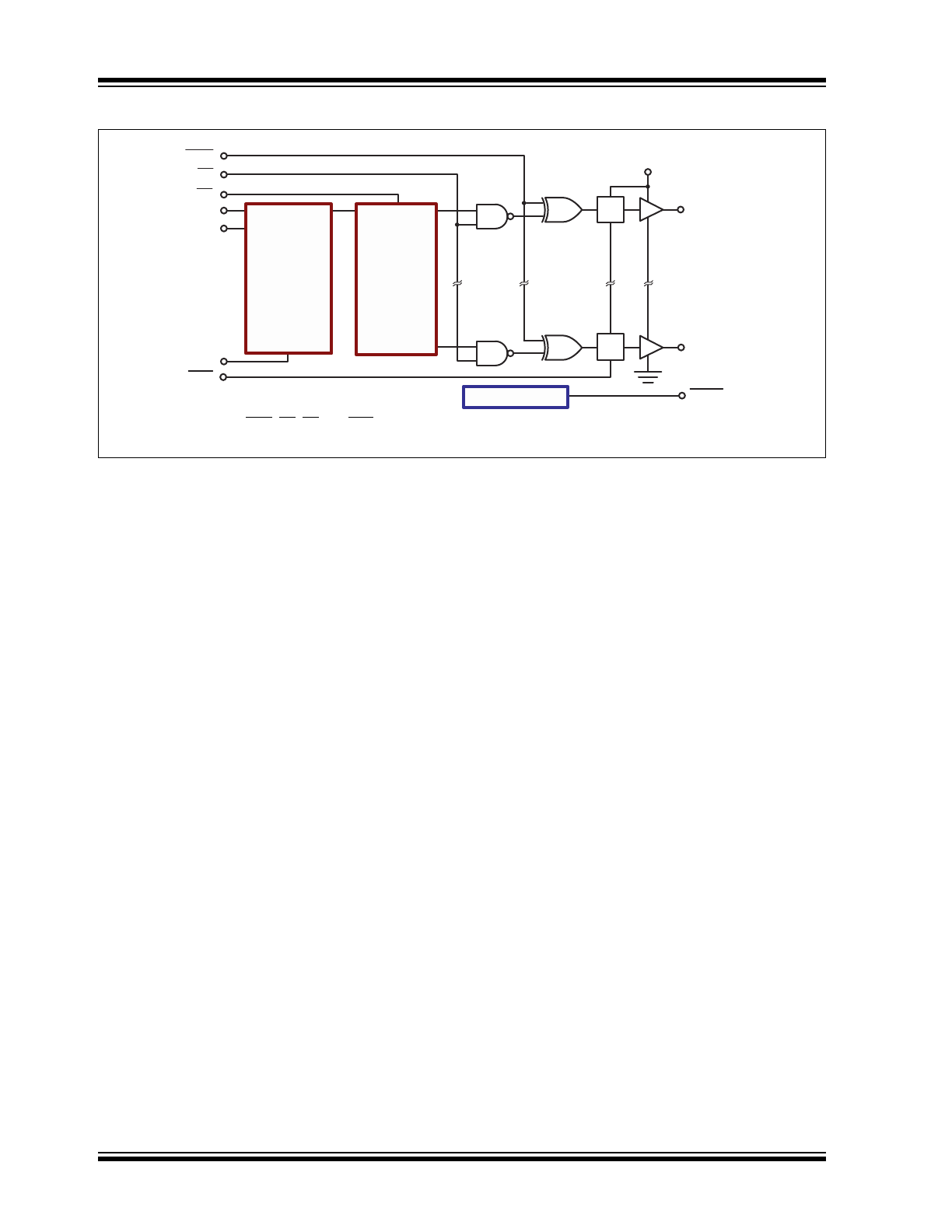
Note 1: POL, BL, LE and Hi-Z have internal 20 k
Ω
pull-up resistors.
POL
BL
CLK
8-Bit
Static
Shift
Register
8 Latches
HV
OUT
1
•
•
•
6 Additional
Outputs
•
•
•
HV
OUT
8
DOUT
DIN
LE
Hi-Z
Short
L/T
L/T
VPP
Short Detect
HV513
DS20005846A-page 2
2017 Microchip Technology Inc.
Functional Block Diagram
2017 Microchip Technology Inc.
DS20005846A-page 3
HV513
Typical Application Circuit
DIN
CLK
DOUT
LE
Hi-Z
POL
HV
OUT
1
HV
OUT
8
High Voltage
Power Supply
HV513
D
IN
to the next HV513 for cascading
Piezo
Element
BL
SHORT
8
/
FPGA
Low Voltage
Power Supply
Low Voltage
Shift Register
Latches
Output
Controller
High Voltage
Level
Translators
&
Push-Pull
Output
Buffers
HV513
DS20005846A-page 4
2017 Microchip Technology Inc.
1.0
ELECTRICAL CHARACTERISTICS
Absolute Maximum Ratings†
Logic Supply Voltage, V
DD
........................................................................................................................ –0.5V to +6V
High-voltage Supply, V
PP
.......................................................................................................................... V
DD
to +275V
Logic Input Levels ........................................................................................................................... –0.5V to V
DD
+0.5V
Ground Current (
Note 1
) ......................................................................................................................................... 0.3A
High-voltage Supply Current (
Note 1
) ................................................................................................................... 0.25A
Maximum Junction Temperature, T
J(MAX)
........................................................................................................... +125°C
Storage Temperature, T
S
.................................................................................................................... –65°C to +150°C
Continuous Total Power Dissipation:
32-lead QFN (
Note 2
) ............................................................................................................................. 750 mW
24-lead SOW (
Note 2
) ............................................................................................................................ 750 mW
† Notice: Stresses above those listed under “Absolute Maximum Ratings” may cause permanent damage to the
device. This is a stress rating only, and functional operation of the device at those or any other conditions above those
indicated in the operational sections of this specification is not intended. Exposure to maximum rating conditions for
extended periods may affect device reliability.
Note 1: Connection to all power and ground pads is required. Duty cycle is limited by the total power dissipated in
the package.
2: For operations above 25°C ambient, derate linearly to 85°C at 12 mW/°C.
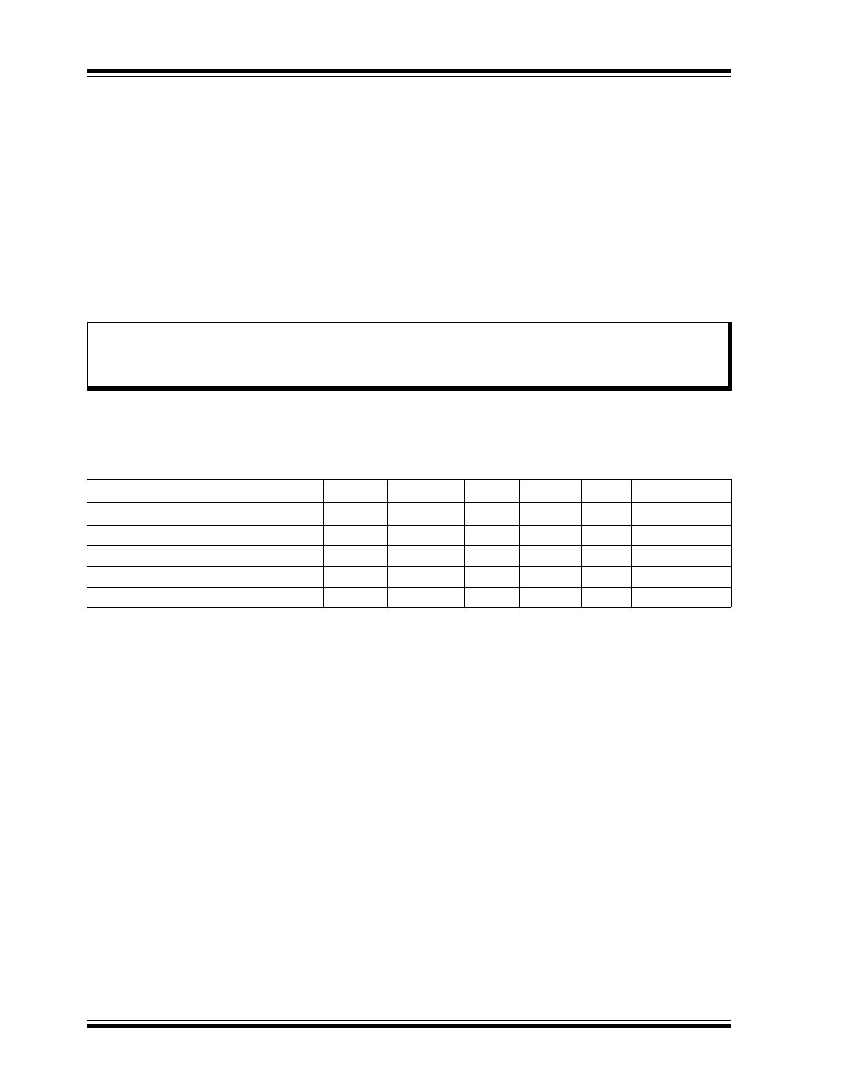
RECOMMENDED OPERATING CONDITIONS
Parameter
Sym.
Min.
Typ.
Max.
Unit
Conditions
Logic Supply Voltage
V
DD
4.5
5
5.5
V
High-voltage Supply Voltage
V
PP
50
—
250
V
Note 1
High-level Input Voltage
V
IH
V
DD
–0.9V
—
V
DD
V
Low-level Input Voltage
V
IL
0
—
0.9
V
Operating Junction Temperature
T
J
–40
—
+85
°C
Note 1: The output may not switch below the minimum V
PP
.
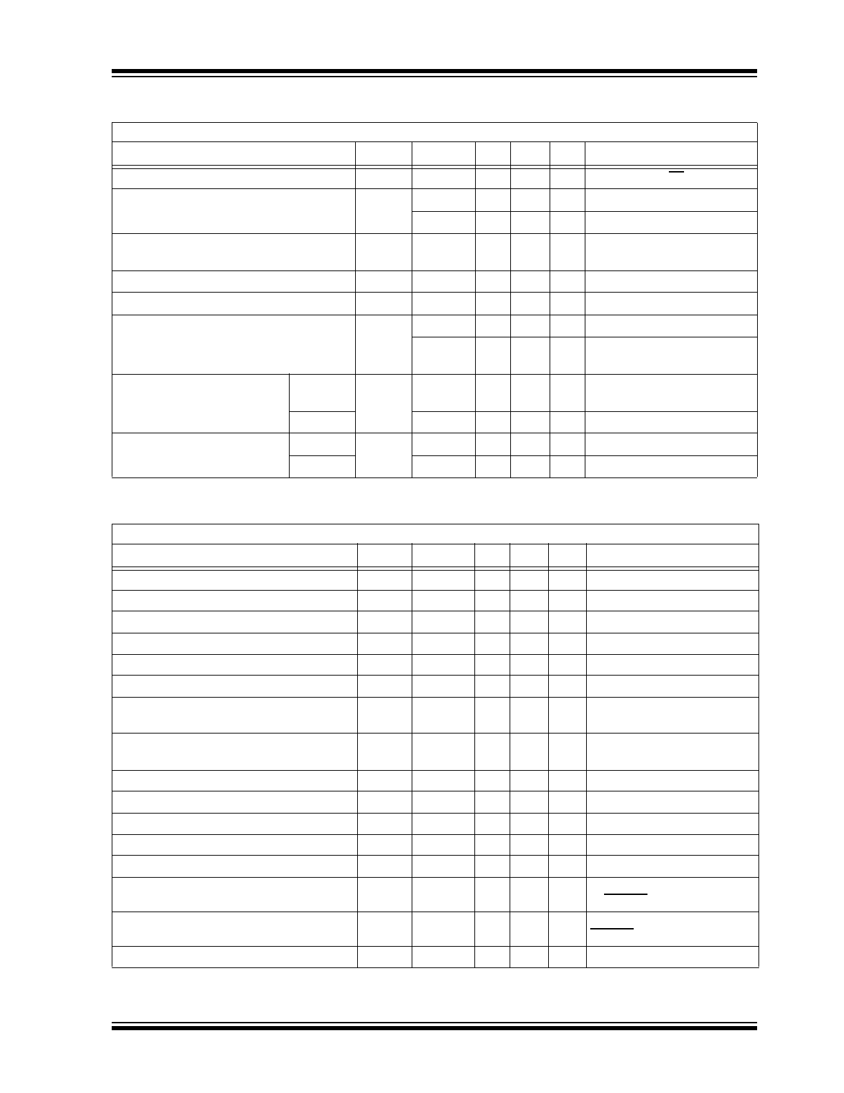
DC ELECTRICAL CHARACTERISTICS
Electrical Specifications: Over typical operating conditions unless otherwise specified, T
J
= 25°C.
Parameter
Sym.
Min.
Typ. Max. Unit
Conditions
V
DD
Supply Current
I
DD
—
—
4
mA f
CLK
= 8 MHz, LE = Low
Quiescent V
DD
Supply Current
I
DDQ
—
—
0.1
mA All V
IN
= V
DD
—
—
2
mA All V
IN
= 0V
High-voltage Supply Current
I
PP
—
—
100
µA
V
PP
= 250V, f
OUT
= 300 Hz,
no load
Quiescent V
PP
Supply Voltage
I
PPQ
—
—
100
µA
V
PP
= 240V, outputs are static
High-level Logic Input Current
I
IH
—
—
10
µA
V
IH
= V
DD
Low-level Logic Input Current
I
IL
—
—
–10
µA
V
IL
= 0V
—
—
–350
µA
V
IL
= 0V, for inputs with
pull-up resistors
High-level Output
HV
OUT
V
OH
140
—
—
V
V
PP
= 200V,
I
HVOUT
= –20 mA
Data Out
V
DD
–1V
—
—
V
I
DOUT
= –0.1 mA
Low-level Output
HV
OUT
V
OL
—
—
60
V
V
DD
= 4.5V, I
HVOUT
= 20 mA
Data Out
—
—
1
V
I
DOUT
= –0.1 mA
AC ELECTRICAL CHARACTERISTICS
Electrical Specifications: Over typical operating conditions unless otherwise specified, T
J
= 25°C.
Parameter
Sym.
Min.
Typ. Max. Unit
Conditions
Clock Frequency
f
CLK
0
—
8
MHz
Output Switching Frequency (SOA Limited)
f
OUT
—
300
—
Hz
C
L
= 50 nF, V
PP
= 200V
Clock Width High and Low
t
WL
, t
WH
62
—
—
ns
Data Set-up Time before Clock Rises
t
SU
15
—
—
ns
Data Hold Time after Clock Rises
t
H
30
—
—
ns
Latch Enable Pulse Width
t
WLE
80
—
—
ns
Latch Enable Delay Time after Rising Edge
of Clock
t
DLE
35
—
—
ns
Latch Enable Set-up Time before Clock
Rises
t
SLE
40
—
—
ns
HV
OUT
Rise/fall Time
t
OR
, t
OF
—
—
1000
µs
C
L
= 100 nF, V
PP
= 200V
Delay Time for Output to Start Rise/fall
t
dON/OFF
—
—
500
ns
Delay Time Clock to Data Low to High
t
DLH
—
—
110
ns
C
L
= 15 pF
Delay Time Clock to Data High to Low
t
DHL
—
—
110
ns
C
L
= 15 pF
All Logic Inputs
t
r
, t
f
—
—
5
ns
Output Short-circuit Detection
t
SD
—
—
500
ns
C
L
= 15 pF, short to output fall
of SHORT
Output Short-circuit Clear
t
SC
—
—
3000
ns
Short clear to output rise of
SHORT
Output High-Z State
t
HI-Z
—
—
500
ns
2017 Microchip Technology Inc.
DS20005846A-page 5
HV513
TEMPERATURE SPECIFICATIONS
Parameter
Sym.
Min.
Typ.
Max.
Unit
Conditions
TEMPERATURE RANGE
Operating Junction Temperature
T
J
–40
—
+85
°C
Maximum Junction Temperature
T
J(MAX)
—
—
+125
°C
Storage Temperature
T
S
–65
—
+150
°C
PACKAGE THERMAL RESISTANCE
32-lead QFN
JA
—
22
—
°C/W
24-lead SOW
JA
—
44
—
°C/W
HV513
DS20005846A-page 6
2017 Microchip Technology Inc.
Timing Waveforms
DATA INPUT
CLK
DATA OUT
LE
HV
OUT
w/S/R Low
HV
OUT
w/S/R High
V
IH
V
IH
V
IH
V
IL
V
IL
V
IL
V
OL
V
OL
V
OL
V
OL
V
OH
V
OH
V
OH
V
OH
50%
50%
50%
50%
50%
50%
50%
50%
50%
50%
90%
10%
10%
90%
Data Valid
t
SU
t
H
t
WH
t
WL
t
DLH
t
DHL
t
SLE
t
WLE
t
DLE
t
OR
t
d(OFF)
t
d(ON)
t
OR
2017 Microchip Technology Inc.
DS20005846A-page 7
HV513
2.0
PIN DESCRIPTION
The details on the pins of HV513 32-lead QFN and
24-lead SOW packages are listed on
Table 2-1
and
Table 2-2
, respectively. Refer to
Package Types
for
the location of pins.
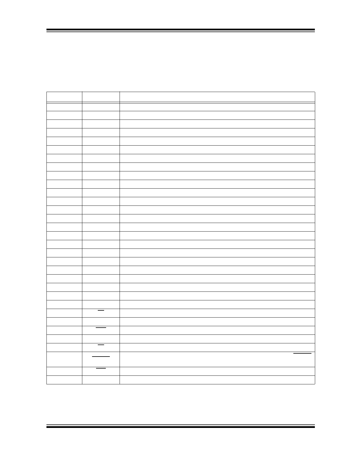
TABLE 2-1:
32-LEAD QFN PIN FUNCTION TABLE
Pin Number
Pin Name
Description
1
NC
No connection
2
NC
No connection
3
NC
No connection
4
LGND
Low-voltage ground
5
HVGND
High-voltage ground
6
HVGND
High-voltage ground
7
NC
No connection
8
NC
No connection
9
HVOUT1
High-voltage push-pull output
10
HVOUT2
High-voltage push-pull output
11
HVOUT3
High-voltage push-pull output
12
HVOUT4
High-voltage push-pull output
13
HVOUT5
High-voltage push-pull output
14
HVOUT6
High-voltage push-pull output
15
HVOUT7
High-voltage push-pull output
16
HVOUT8
High-voltage push-pull output
17
NC
No connection
18
NC
No connection
19
VPP
High-voltage supply
20
VPP
High-voltage supply
21
VDD
Logic supply voltage
22
DOUT
Data output
23
NC
No connection
24
NC
No connection
25
BL
Blanking. A logic input low sets all HVOUTs low.
26
NC
No connection
27
POL
Polarity bar input logic
28
CLK
Clock. Shift registers shift data on the rising edge of input clock.
29
LE
Latch enable bar input logic
30
SHORT
If output does not reach its required state, a logic‘0’will be asserted at the SHORT
pin.
31
Hi-Z
High-impedance pin. Logic input low sets all outputs in a high-impedance state.
32
DIN
Data input
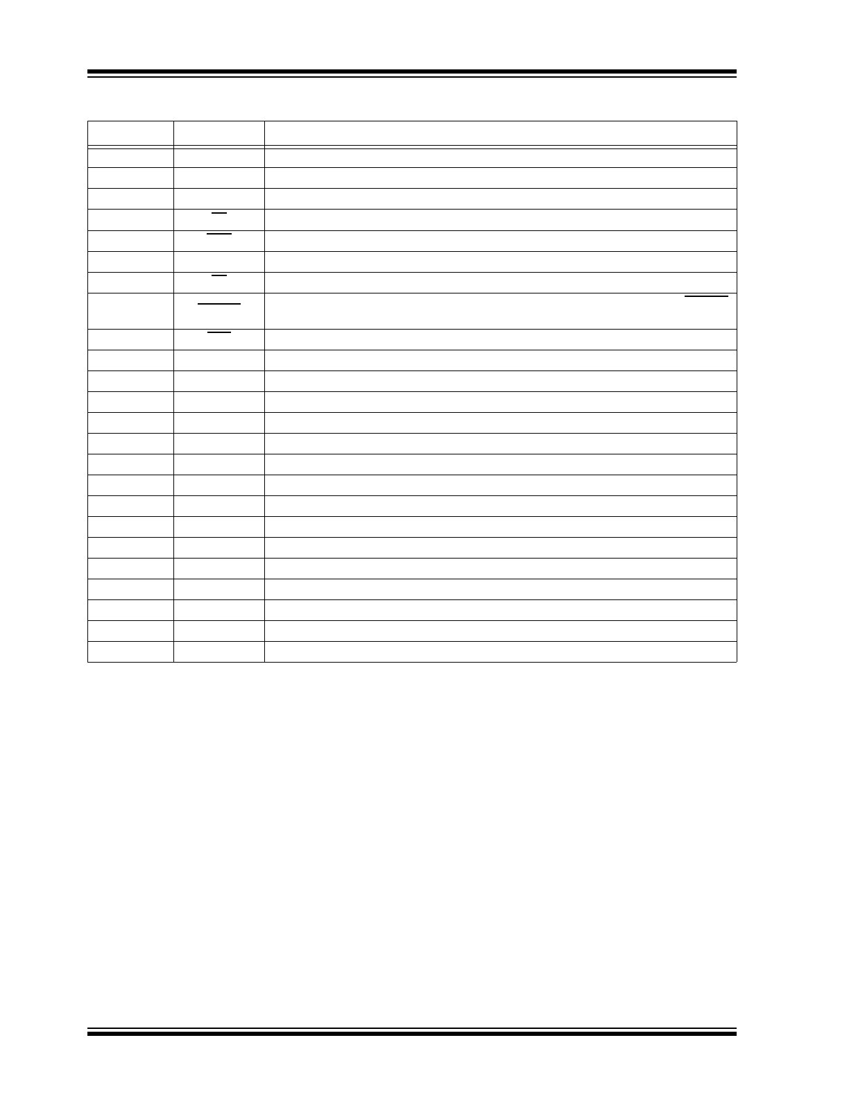
TABLE 2-2:
24-LEAD SOW PIN FUNCTION TABLE
Pin Number
Pin Name
Description
1
NC
No connection
2
VDD
Logic supply voltage
3
DOUT
Data output
4
BL
Blanking. A logic input low sets all HVOUTs low.
5
POL
Polarity bar input logic
6
CLK
Clock. Shift registers shift data on the rising edge of input clock.
7
LE
Latch enable bar input logic
8
SHORT
If output does not reach its required state, a logic‘0’will be asserted at the SHORT
pin.
9
Hi-Z
High-impedance pin. Logic input low sets all outputs in a high-impedance state.
10
DIN
Data input
11
LGND
Low-voltage ground
12
NC
No connection
13
HVGND
High-voltage ground
14
HVGND
High-voltage ground
15
HVOUT1
High-voltage push-pull output
16
HVOUT2
High-voltage push-pull output
17
HVOUT3
High-voltage push-pull output
18
HVOUT4
High-voltage push-pull output
19
HVOUT5
High-voltage push-pull output
20
HVOUT6
High-voltage push-pull output
21
HVOUT7
High-voltage push-pull output
22
HVOUT8
High-voltage push-pull output
23
VPP
High-voltage supply
24
VPP
High-voltage supply
HV513
DS20005846A-page 8
2017 Microchip Technology Inc.
2017 Microchip Technology Inc.
DS20005846A-page 9
HV513
3.0
FUNCTIONAL DESCRIPTION
Follow the steps in
Table 3-1
to power up and power
down the HV513.
TABLE 3-1:
POWER-UP AND POWER-DOWN SEQUENCE
Power-up
Power-down
Step
Description
Step
Description
1
Connect ground.
1
Remove V
PP.
2
Apply V
DD.
2
Remove all inputs.
3
Set all inputs (Data, CLK, Enable, etc.) to a known state.
3
Remove V
DD.
4
Apply V
PP.
4
Disconnect ground.
TABLE 3-2:
Function
Inputs
Outputs
Data CLK
LE
BL POL Hi-Z
Shift Register
High-voltage Output
Data Out
1
2...8
1
2...8
*
All On
X
X
X
L
L
H
*
*...*
H
H...H
*
All Off
X
X
X
L
H
H
*
*...*
L
L...L
*
Invert Mode
X
X
L
H
L
H
*
*...*
*
*...*
*
Load S/R
H or L
↑
L
H
H
H
H or L
*...*
*
*...*
*
Store Data in
Latches
X
X
L
H
H
H
*
*...*
*
*...*
*
X
X
L
H
L
H
*
*...*
*
*...*
*
Transparent
Latch Mode
L
↑
H
H
H
H
L
*...*
L
*...*
*
H
↑
H
H
H
H
H
*...*
H
*...*
*
Outputs Hi-Z
X
X
X
X
X
L
*
*...*
High-impedance outputs
*
Outputs On
X
X
X
X
X
H
*
*...*
*
*...*
*
Note:
H = High-logic level
L = Low-logic level
X = Irrelevant
↑ = Low-to-high transition
* = Dependent on the previous stage’s state before the last CLK or last LE high
TRUTH FUNCTION TABLE
VDD
INPUT
GND
VDD
DATA OUT
VPP
HV
OUT
HVGND
GND
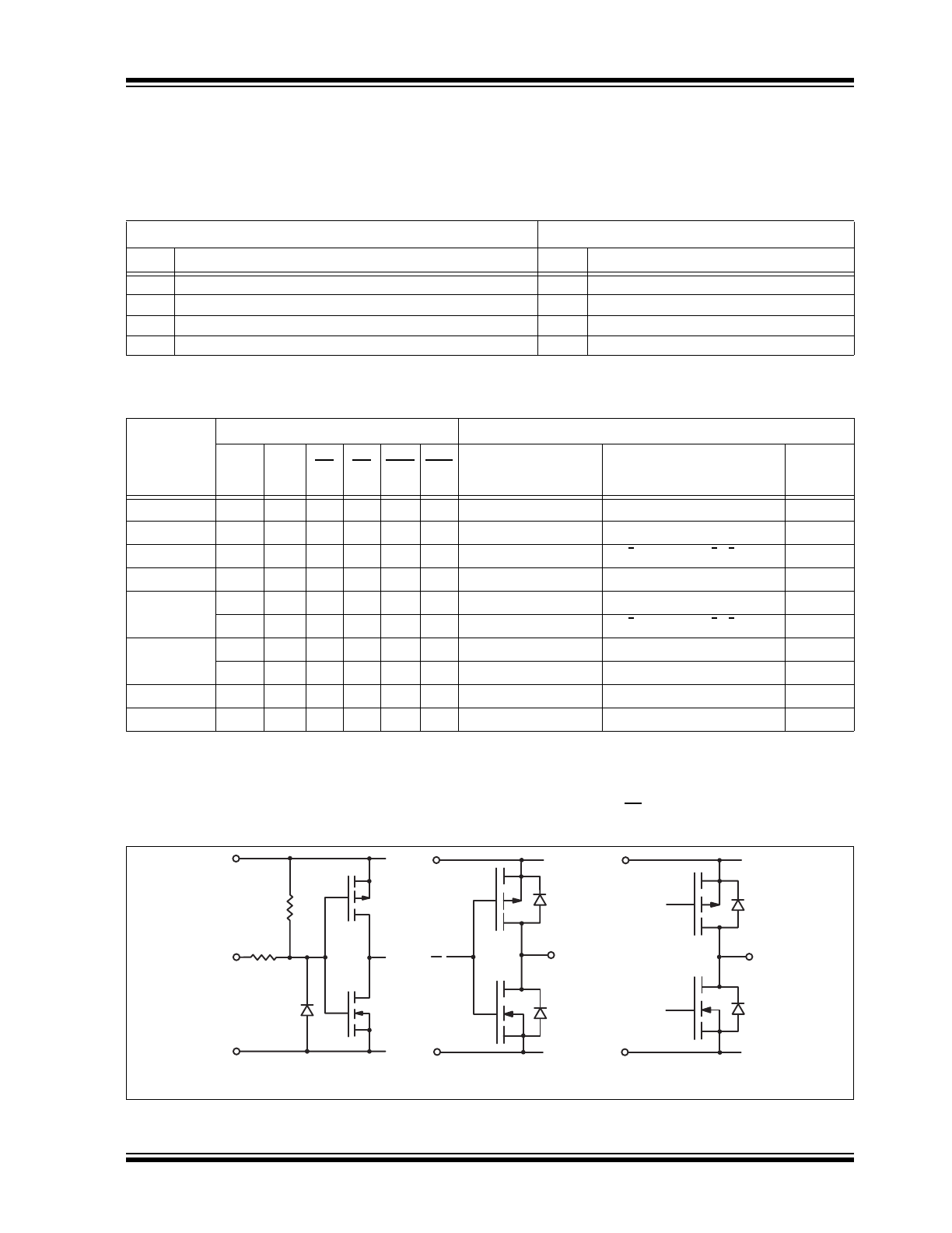
Logic Inputs
High Voltage Outputs
Logic Data Output
20kΩ*
FIGURE 3-1:
Input and Output Equivalent Circuits.
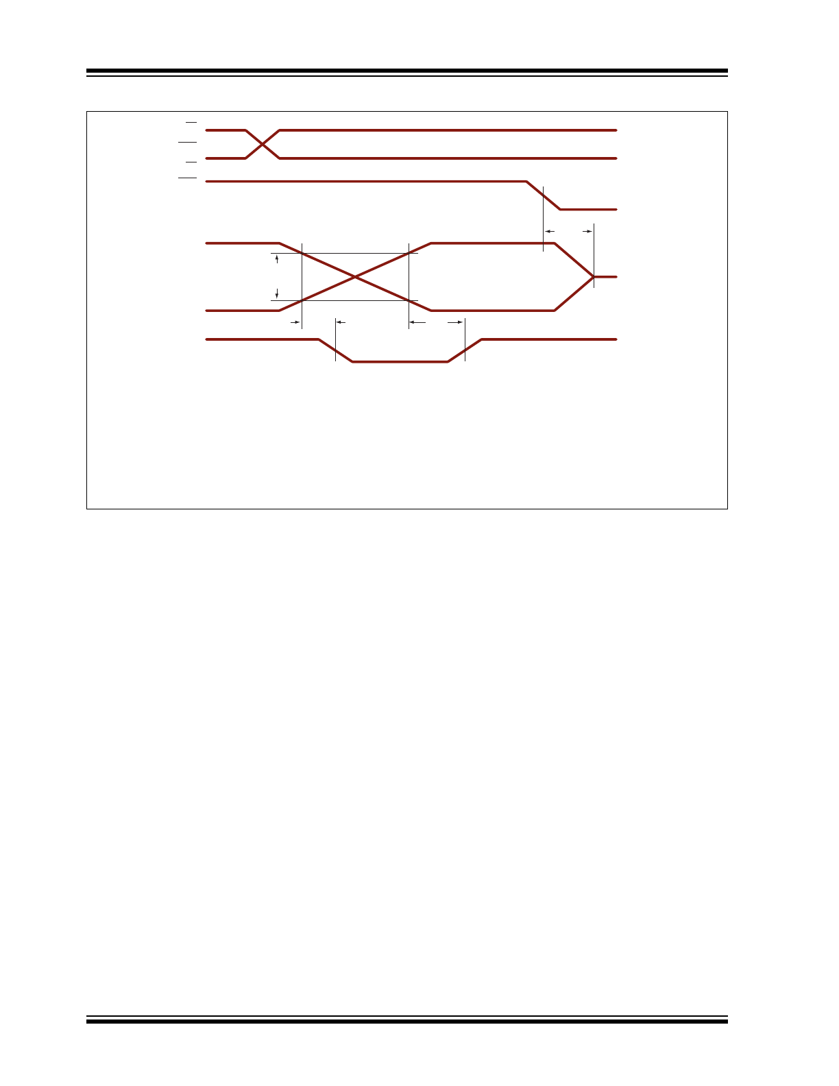
Note 1: For V
PP
greater than 150V, the short detect output will flag short conditions.
There are two possibilities:
Case 1: HV
OUT
is higher than 10V when expected low.
Case 2: H
VOUT
is lower than V
P
–100V when expected high.
2: For V
PP
greater than 150V, the short detect output will stay clear. There are two
possibilities:
Case 1: HV
OUT
is lower than 2V when expected low.
Case 2: HV
OUT
is higher than V
PP
–60V when expected high.
LE
POL
BL
HI-Z
HV
OUT
Within
xV of rail
Short
Detect
V
IH
V
IH
V
IL
V
IL
V
IL
V
IH
V
OH
V
OL
t
Hi-Z
t
SD
t
SC
HV513
DS20005846A-page 10
2017 Microchip Technology Inc.
FIGURE 3-2:
Short-circuit Detect Detail Timing.