
2017 Microchip Technology Inc.
DS20005728A-page 1
HV508
Features
• Logic-selectable Output Voltage
• 100 nF Drive Capability
• 90 V
P-P
Maximum Output Voltage
• 25 µs Response Time
Applications
• Liquid Crystal Shutter
General Description
The HV508 is a 45V liquid crystal shutter driver in an
8-lead SOIC surface-mount package. It is composed of
two outputs that provide square waves of opposite
phases. The liquid crystal shutter is connected
between the two outputs. Its equivalent load can be
modeled as a minimum of 1 MΩ resistor in parallel with
a maximum of 0.1 uF capacitor.
The HV508 has three input supply voltages—HV
IN
,
LV
IN
and V
DD
. The output amplitude is either LV
IN
or
HV
IN
. A logic high on the HV
EN
input sets the output to
operate from the HV
IN
supply. On the other hand, a
logic low on the HV
EN
input sets the output to operate
from the LV
IN
supply. The output frequency is
determined by the logic input frequency applied to the
POL input.
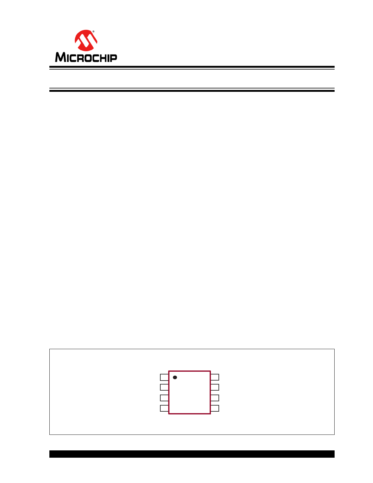
Package Type
See
Table 2-1
for pin information.
8-lead SOIC
(Top view)
1
2
3
4
8
7
6
5
LVIN
POL
HVEN
GND
HVOUT1
HVIN
VDD
HVOUT2
High-Voltage Liquid Crystal Shutter Driver
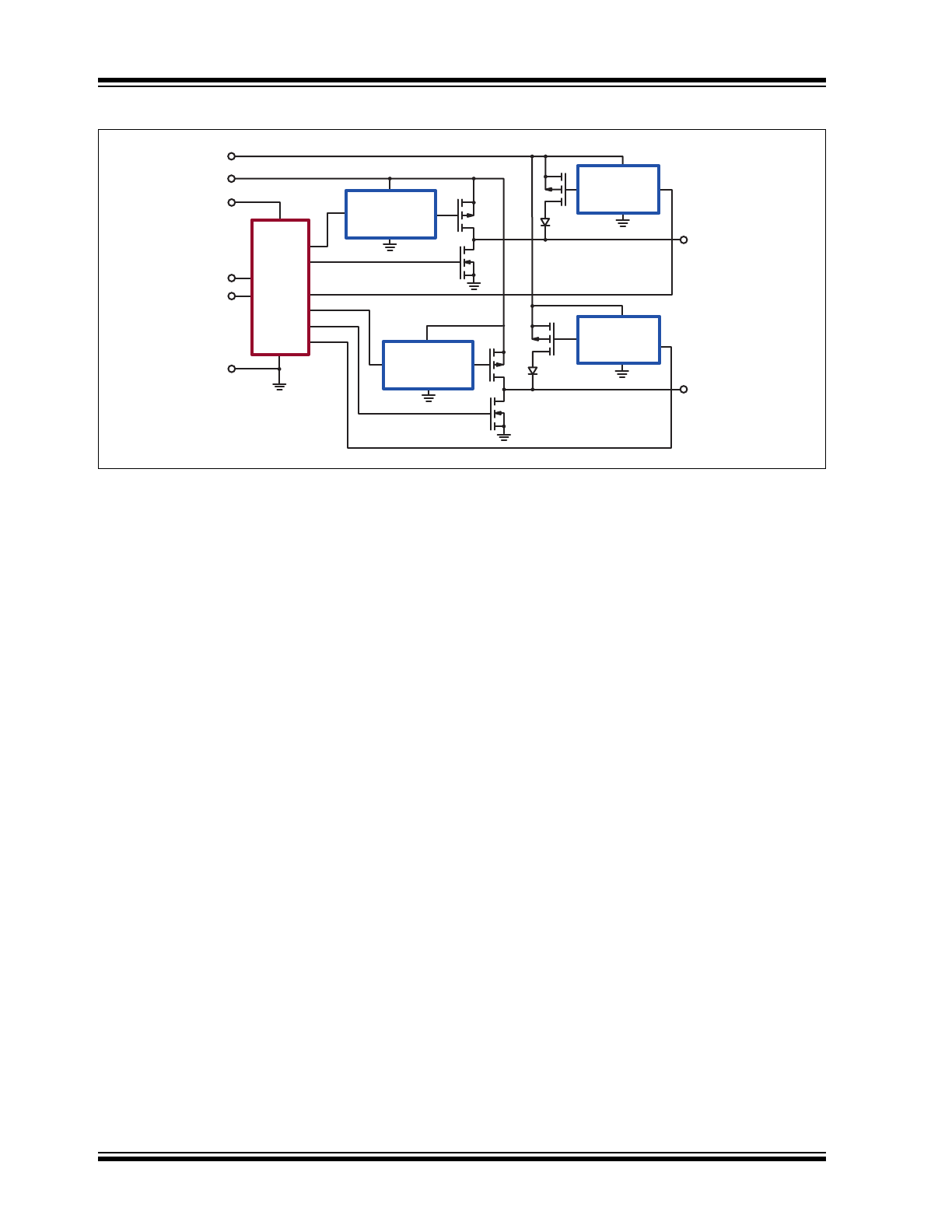
LVIN
HVIN
VDD
HVEN
POL
GND
HV
OUT
1
HV
OUT
2
Level
Translator
Level
Translator
Level
Translator
Level
Translator
CMOS
Logic
HV508
DS20005728A-page 2
2017 Microchip Technology Inc.
Functional Block Diagram
2017 Microchip Technology Inc.
DS20005728A-page 3
HV508
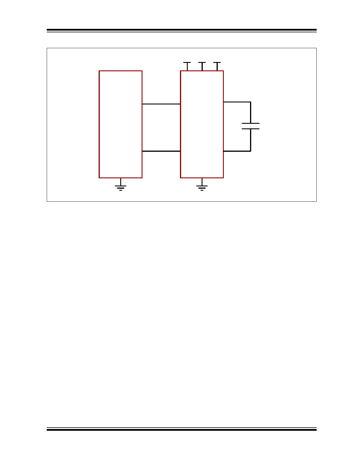
Typical Application Circuit
HVIN
Image
Controller
HV508
HVEN
POL
Liquid
Crystal
Shutter
HV
OUT
1
HV
OUT
2
VDD LVIN
HV508
DS20005728A-page 4
2017 Microchip Technology Inc.
1.0
ELECTRICAL CHARACTERISTICS
Absolute Maximum Ratings†
High-voltage Input, HV
IN
......................................................................................................................................... +60V
Low-voltage Input, LV
IN
......................................................................................................................................... +7.5V
Logic Supply voltage, V
DD
....................................................................................................................................... +12V
Operating Ambient Temperature, T
A
....................................................................................................... –5°C to +60°C
Storage Temperature, T
S
.................................................................................................................... –65°C to +150°C
Power Dissipation (
Note 1
):
8-lead SOIC ............................................................................................................................................ 700 mW
† Notice: Stresses above those listed under “Absolute Maximum Ratings” may cause permanent damage to the
device. This is a stress rating only, and functional operation of the device at those or any other conditions above those
indicated in the operational sections of this specification is not intended. Exposure to maximum rating conditions for
extended periods may affect device reliability.
Note 1: For operation above 25°C ambient, derate linearly at 6 mW/°C.
RECOMMENDED OPERATING CONDITIONS
Parameter
Sym.
Min.
Typ.
Max.
Unit
Conditions
Logic Supply Voltage
V
DD
5
—
10
V
Low-output Supply Voltage
LV
IN
3
—
6
V
High-output Supply Voltage
H
VIN
5
—
45
V
Logic Input Voltage Low
V
IL
0
—
0.3 V
DD
V
Logic Input Voltage High
V
IH
0.7 V
DD
—
V
DD
V
Ambient Temperature
T
A
–5
—
+60
°C
DC ELECTRICAL CHARACTERISTICS
Electrical Specifications: Over operating supply voltages; T
A
= –5°C to +60°C unless otherwise indicated.
Parameter
Sym.
Min.
Typ.
Max.
Unit
Conditions
HV
IN
Quiescent Current
I
HVQ
—
—
10
µA
LV
IN
Quiescent Current
I
LVQ
—
—
10
µA
V
DD
Quiescent Current
I
DDQ
—
—
10
µA
HV
IN
Operating Current
I
HV
—
—
2.8
mA
POL = 100 Hz, HV
EN
= high,
T
A
= 25°C, Load = 1 MΩ in parallel
with 0.1 µF between HV
OUT
1 and
HV
OUT
2
LV
IN
Operating Current
I
LV
—
—
380
µA
POL = 100 Hz, HV
EN
= low,
T
A
= 25°C, Load = 1 MΩ in parallel
with 0.1 µF between HV
OUT
1 and
HV
OUT
2
Logic Input Current Low
I
IL
–5
—
—
µA
Logic Input Current High
I
IH
—
—
5
µA
Output Capacitive Load
C
LOAD
0
—
0.25
µF
C
LOAD
in parallel with a 1 MΩ
resistor (
Note 1
)
Note 1: The device can operate continuously in this range without damage. AC limits are not implemented.
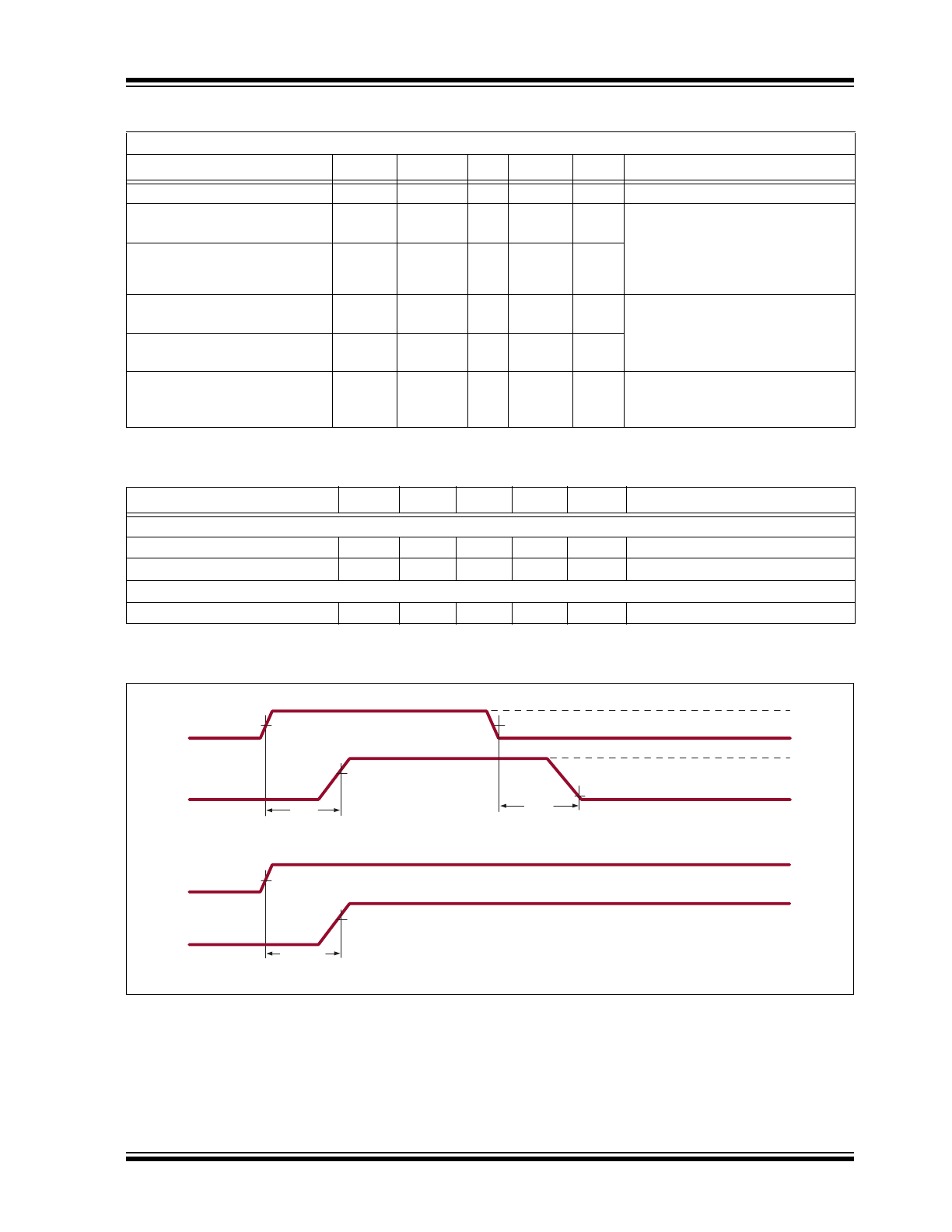
AC ELECTRICAL CHARACTERISTICS
Electrical Specifications: HV
IN
= 45V, LV
IN
= 6V, V
DD
= 5V, and T
A
= –5°C to +60°C.
Parameter
Sym.
Min.
Typ.
Max.
Unit
Conditions
POL Input Frequency
f
POL
0
—
100
Hz
Turn-on Time when
High-voltage is Enabled
t
HV(ON)
—
—
16
µs
Load = 1 MΩ in parallel with
0.1 µF between HV
OUT
1 and
HV
OUT
2, HV
EN
= high, outputs rise
to HV
IN
(See Fig.1 in
Timing Wave-
forms
.)
Turn-off Time when
high-voltage is Enabled
t
HV(OFF)
—
—
16
µs
Turn-on time when
High-voltage is Disabled
t
LV(ON)
—
—
40
µs
Load = 1 MΩ in parallel with 0.1 µF
between HV
OUT
1 and HV
OUT
2,
HV
EN
= low, outputs rise to HV
IN
(See Fig.1 in
Timing Waveforms
.)
Turn-off time when
High-voltage is Disabled
t
LV(OFF)
—
—
6
µs
Turn-on time from HV
EN
to
HV
OUT
t
EN(ON)
—
—
25
µs
Load = 1 MΩ in parallel with 0.1 µF
between HV
OUT
1 and HV
OUT
2
(See Fig.2 in
Timing Waveforms
.)
TEMPERATURE SPECIFICATIONS
Parameter
Sym.
Min.
Typ.
Max.
Unit
Conditions
TEMPERATURE RANGE
Operating Ambient Temperature
T
A
–5
—
+60
°C
Storage Temperature
T
S
–65
—
+150
°C
PACKAGE THERMAL RESISTANCE
8-lead SOIC
JA
—
101
—
°C/W
2017 Microchip Technology Inc.
DS20005728A-page 5
HV508
Timing Waveforms
50%
80%
5%
50%
t
(OFF)
t
(ON)
POL
HV
OUT
1
GND
V
IL
V
IH
HV
IN
or LV
IN
50%
80%
HV
EN
HV
OUT
1
LV
IN
V
IL
V
IH
HV
IN
t
(ENON)
Fig. 1
Fig. 2
HV508
DS20005728A-page 6
2017 Microchip Technology Inc.
2.0
PIN DESCRIPTION
The details on the pins of HV508 are listed on
Table 2-1
. Refer to
Package Type
for the location of
pins.
TABLE 2-1:
PIN FUNCTION TABLE
Pin Number
Pin Name
Description
1
LVIN
Low Voltage Supply
2
POL
Polarity
3
HVEN
High Voltage Enable
4
GND
Ground
5
HVOUT2
High Voltage Output Channel 2
6
VDD
Logic Voltage Supply
7
HVIN
High Voltage Supply
8
HVOUT1
High Voltage Output Channel 1
2017 Microchip Technology Inc.
DS20005728A-page 7
HV508
3.0
FUNCTIONAL DESCRIPTION
Follow the steps in
Table 3-1
to power up and power
down the HV508.
TABLE 3-1:
POWER-UP AND POWER-DOWN SEQUENCE
Power-up
Power-down
Step
Description
Step
Description
1
Connect ground.
1
Remove LV
IN.
2
Apply V
DD
.
2
Remove H
VIN
.
3
Connect logic Inputs.
2
Remove all logic inputs.
4
Connect HV
IN.
3
Remove V
DD
.
5
Connect LV
IN.
4
Disconnect ground.
TABLE 3-2:
TRUTH FUNCTION TABLE
HV
EN
POL
HV
OUT
1
HV
OUT
2
H
H
HV
IN
GND
H
L
GND
HV
IN
L
H
LV
IN
GND
L
L
GND
LV
IN
HV508
DS20005728A-page 8
2017 Microchip Technology Inc.
4.0
PACKAGE MARKING INFORMATION
4.1
Packaging Information
Legend: XX...X
Product Code or Customer-specific information
Y
Year code (last digit of calendar year)
YY
Year code (last 2 digits of calendar year)
WW
Week code (week of January 1 is week ‘01’)
NNN
Alphanumeric traceability code
Pb-free JEDEC
®
designator for Matte Tin (Sn)
*
This package is Pb-free. The Pb-free JEDEC designator ( )
can be found on the outer packaging for this package.
Note:
In the event the full Microchip part number cannot be marked on one line, it will
be carried over to the next line, thus limiting the number of available
characters for product code or customer-specific information. Package may or
not include the corporate logo.
3
e
3
e
8-lead SOIC
Example
NNN
XXXXXXXX
YYWW
e3
897
HV508LG
1718
e3
Note: For the most current package drawings, see the Microchip Packaging Specification at www.microchip.com/packaging.
2017 Microchip Technology Inc.
DS20005728A-page 9
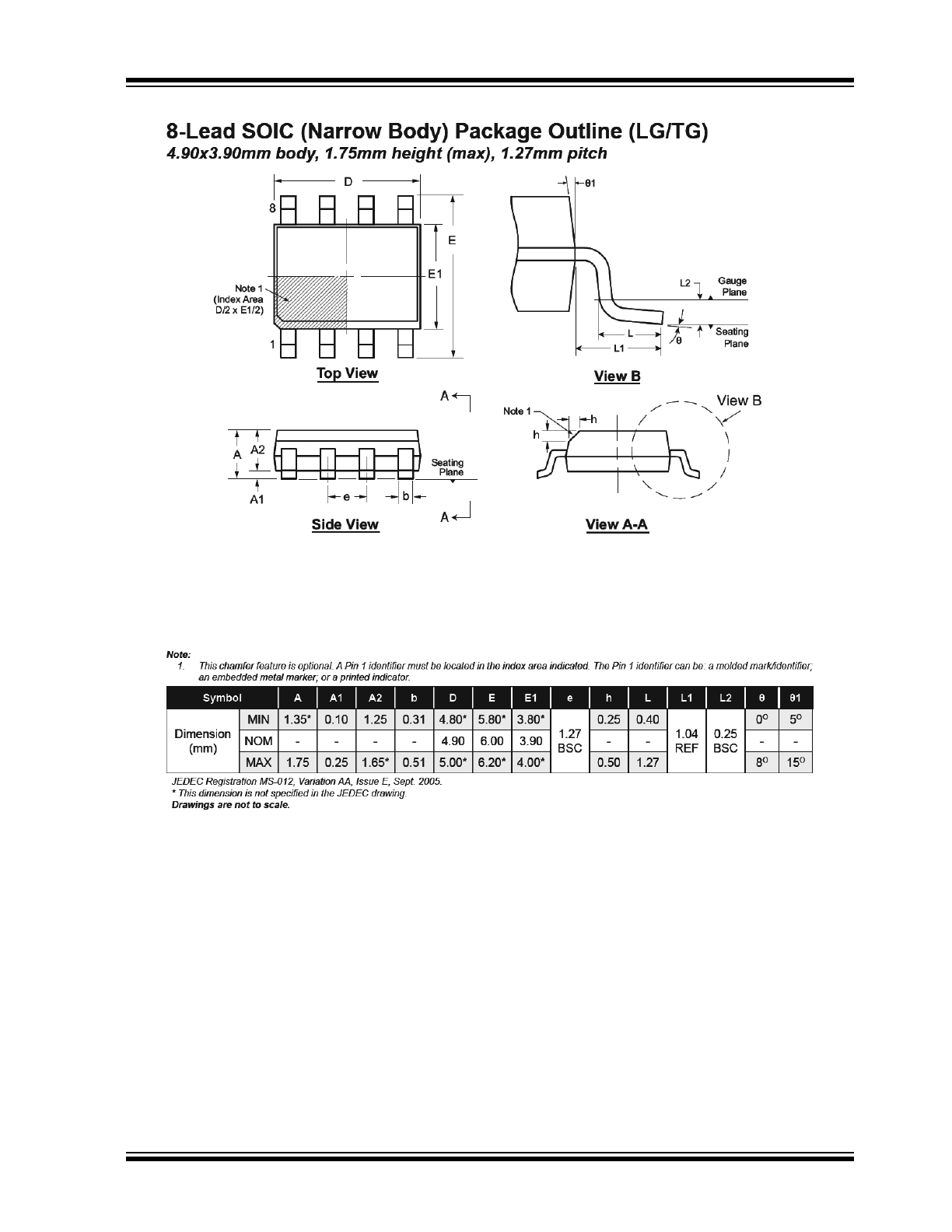
HV508

HV508
DS20005728A-page 10
2017 Microchip Technology Inc.
NOTES: