
2017 Microchip Technology Inc.
DS20005721A-page 1
HV2803/HV2903/HV2904
Features
• 32-Channel, High-Voltage Analog Switch
• No High-Voltage Supplies Required
• 32-Channel, Single-Pole, Single-Throw (SPST)
Individual Switching or Bank Switching
• 3.3V CMOS Input Logic Level
• 66 MHz Data Shift Clock Frequency
• Silicon-on-Insulator (SOI) High-Voltage
Technology for High Performance
• Standby mode for Low-Power Dissipation
• Low-Parasitic Capacitance
• DC to 50 MHz Analog Small-Signal Frequency
• 200 kHz to 50 MHz Large-Signal Frequency
• -70 dB Typical Off Isolation at 5.0 MHz
• Excellent Noise Immunity
• Cascadable Serial Data Register with Latches
• Integrated Bleed Resistors on the Outputs (both
sides for HV2903, one side for HV2904)
Applications
• Medical Ultrasound Imaging
• Non-Destructive Testing (NDT) Metal Flaw
Detection
• Piezoelectric Transducer Drivers
• Inkjet Printer Heads
• Optical MEMS Modules
General Description
The HV2803/HV2903/HV2904 devices are low harmonic
distortion, low charge injection, 32-channel, high-voltage
analog switches without high-voltage supplies. They are
intended for use in applications requiring high-voltage
switching controlled by low-voltage control signals, such
as medical ultrasound imaging, driving piezoelectric
transducers and printers.
The HV2903 device has integrated bleed resistors at
both sides of the switches; the HV2904 device has
bleed resistors at one side only, while the HV2803
device has no bleed resistors. The bleed resistor
eliminates voltage build-up on capacitive loads, such
as piezoelectric transducers.
The HV2803/HV2903/HV2904 devices have two
modes of operation determined by the MODE pin input.
MODE input high enables an individual Switching
mode of 32-channel SPST switches and MODE input
low enables a Bank Switching mode of 16-Pole
Double-Throw (16PDT) switches to support bank
switching for probe selection.
The devices require only ±6V or ±5V low-voltage sup-
plies and no high-voltage supplies. However, all of the
analog switches can transmit ±100V high-voltage pulses.
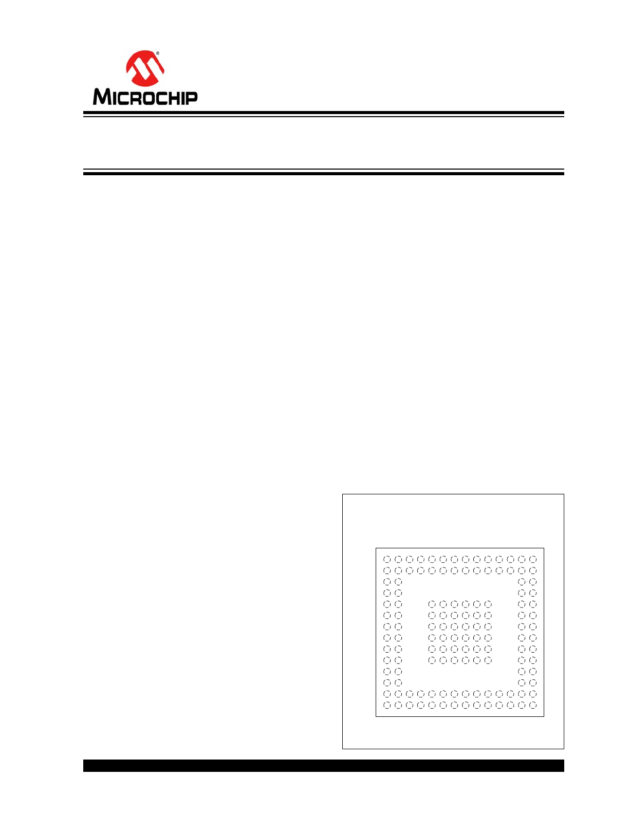
Package Type
1
2
3
4
5
6
7
8
9
10 11 12 13
A
B
C
D
E
F
G
H
P
J
K
L
M
14
N
HV2803/HV2903/HV2904
12 x 12 x 1.20 mm TFBGA
(Top View
*
)
* See
Section 2.0 “Package Pin Configuration
and Function Description”
.
No High-Voltage Bias, Low Harmonic Distortion,
32-Channel, High-Voltage Analog Switch
HV2803/HV2903/HV2904
DS20005721A-page 2
2017 Microchip Technology Inc.
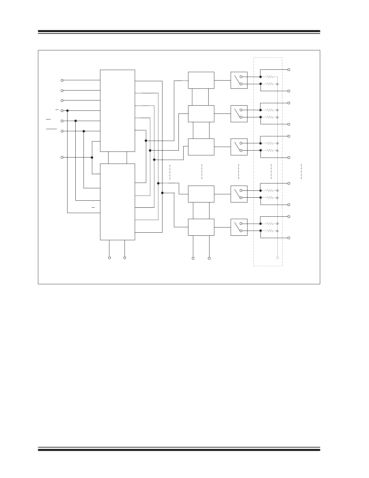
Block Diagram
Level
Shifters
V
DD
V
SS
Output
Switches
SW0A
SW0B
SW1A
SW1B
SW2A
SW2B
SW30A
SW30B
SW31A
SW31B
Bleed
Resistors
R
GND
HV2903 has bleed resistor at SWxA and SWxB
HV2904 has bleed resistor at SWxA only
GND
V
LL
CLR
LE/EN
CLK
D
IN
/AB
D
OUT
32-Bit
Shift
Register
and
Latches
(Mode = H,
Individual
Switching Logic)
Logic
Control
and
Latches
(Mode = L,
Bank Switching
Logic)
EN
A/B
MODE
STBY
2017 Microchip Technology Inc.
DS20005721A-page 3
HV2803/HV2903/HV2904
1.0
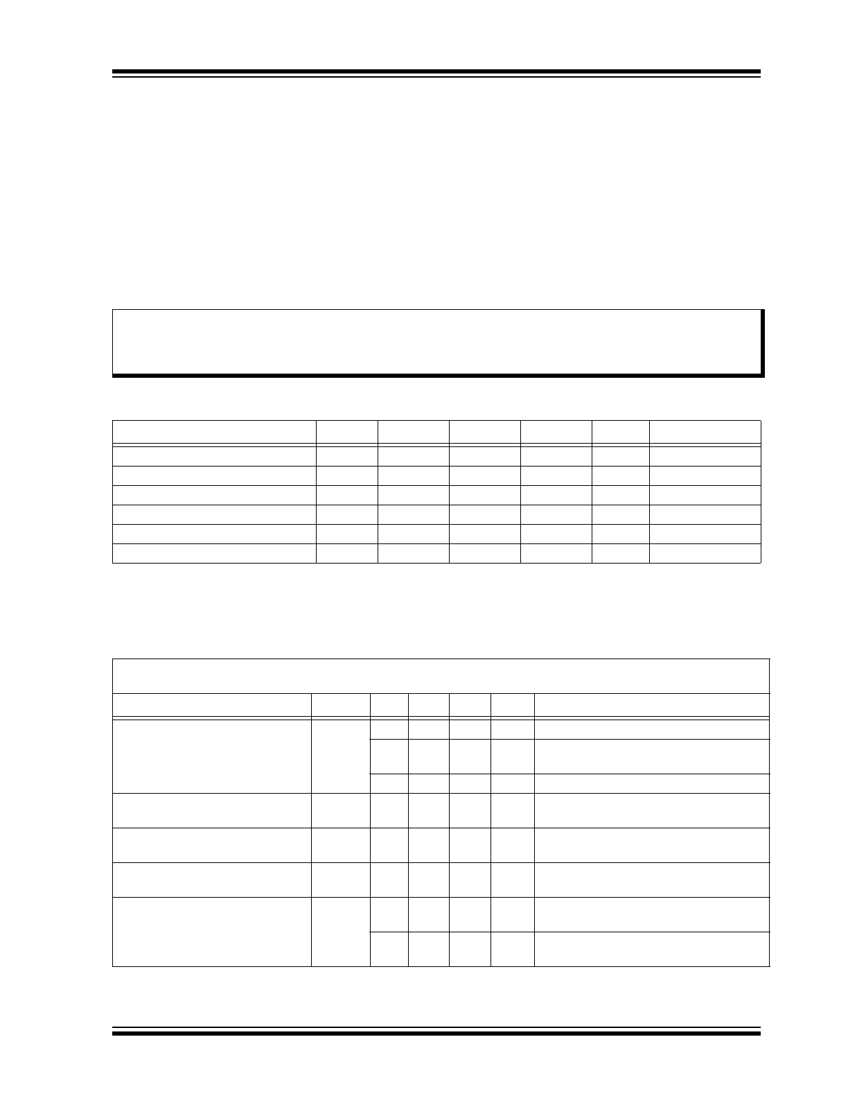
ELECTRICAL CHARACTERISTICS
Absolute Maximum Ratings†
Logic Supply Voltage (V
LL
)......................................................................................................................... -0.5V to +6.6V
Positive Supply Voltage (V
DD
).................................................................................................................... -0.5V to +6.6V
Negative Supply Voltage (V
SS
) .................................................................................................................. +0.5V to -6.6V
Logic Input Voltage (V
IN
).....................................................................................................................-0.5V to V
LL
+ 0.3V
DGND to GND ........................................................................................................................................... -0.3V to +0.3V
Analog Signal Range (V
SIG
)......................................................................................................................-110V to +110V
Peak Analog Signal Current/Channel (I
PK
) ...................................................................................................................3A
† Notice:
Stresses above those listed under “Maximum Ratings” may cause permanent damage to the device. This is
a stress rating only and functional operation of the device at those or any other conditions above those indicated in the
operational sections of this specification is not intended. Exposure to maximum rating conditions for extended periods
may affect device reliability.
RECOMMENDED OPERATING CONDITIONS
(
1
,
2
,
3
)
Parameters
Sym.
Min.
Typ.
Max.
Units
Conditions
Logic Supply Voltage
V
LL
3
—
3.6
V
Positive Supply Voltage
V
DD
4.5
—
6.3
V
Negative Supply Voltage
V
SS
-6.3
—
-4.5
V
High-Level Input Voltage
V
IH
0.9 V
LL
—
V
LL
V
Low-Level Input Voltage
V
IL
0
—
0.1 V
LL
V
Analog Signal Voltage Peak-to-Peak
V
SIG
-100
—
100
V
Note 1:
Power-up sequence is V
SS
, V
DD
and then V
LL
. Power-down sequence is the reverse of power-up.
2:
V
SIG
must be V
SS
≤ V
SIG
≤ V
DD
or floating during power-up/down transition.
3:
Rise and fall times of power supplies, V
LL
, V
DD
and V
SS
should be greater than 1.0 ms.
DC ELECTRICAL CHARACTERISTICS
Unless otherwise specified, V
DD
= 6.0V, V
SS
= -6.0V, V
LL
= 3.3V, T
AMB
= +25°C. Boldface specifications apply over
the full operating temperature range.
Parameters
Sym.
Min.
Typ.
Max.
Units
Conditions
Small-Signal Switch
On-Resistance
R
ONS
—
10
15
I
SIG
= 5 mA
—
10.4
—
V
DD
= +5V, V
SS
= -5V, I
SIG
= 5 mA
(
Note 1
)
—
10
15
I
SIG
= 200 mA
Small-Signal Switch
On-Resistance Matching
ΔR
ONS
—
5
20
%
I
SIG
= 5 mA
Large-Signal Switch
On-Resistance
R
ONL
—
9
—
V
SIG
= 90V, I
SIG
= 1A
(
Note 1
)
Value of Output Bleed Resistor
(HV2903/HV2904 only)
R
INT
20
35
50
k
Output switch to R
GND
,
I
RINT
= 0.1 mA
Switch Off Leakage per SW
I
SOL
—
—
3
µA
At 49 µs with V
SIG
= +100V,
50 μs pulse (see
Figure 3-1
)
—
—
3
µA
At 49 μs with V
SIG
= -100V,
50 μs pulse (see
Figure 3-1
)
Note 1:
Specification is obtained by characterization and is not 100% tested.
2:
Design guidance only.
HV2803/HV2903/HV2904
DS20005721A-page 4
2017 Microchip Technology Inc.
HV2803
Switch Off Bias per SW
I
SOB
—
—
3
μA
V
SIG
= +100V, 400 μs pulse
(see
Figure 3-2
)
—
—
4
mA
V
SIG
= -100V, 12 μs pulse
(see
Figure 3-2
) (
Note 1
)
HV2903
Switch Off Bias per SW
I
SOB
—
—
3
μA
V
SIG
= +100V, 400 μs pulse
(see
Figure 3-2
)
—
—
8
mA
V
SIG
= -100V, 12 μs pulse
(see
Figure 3-2
) (
Note 1
)
HV2904
Switch Off Bias per SWA
(with bleed resistor)
I
SOB
—
—
3
μA
V
SIG
= +100V, 400 μs pulse
(see
Figure 3-2
)
—
—
8
mA
V
SIG
= -100V, 12 μs pulse
(see
Figure 3-2
) (
Note 1
)
Switch Off Bias per SWB
(without bleed resistor)
—
—
3
μA
V
SIG
= +100V, 400 μs pulse
(see
Figure 3-2
)
—
—
4
mA
V
SIG
= -100V, 12 μs pulse
(see
Figure 3-2
) (
Note 1
)
Switch Off DC Offset
V
OS
—
1
10
mV
R
LOAD
= 25 k
(HV2803), 50 k(HV2904)
No load (HV2903) (see
Figure 3-3
)
Switch On DC offset
—
1
10
Quiescent V
DD
Supply Current
I
DDQ
—
—
7
mA
All switches off
Quiescent V
SS
Supply Current
I
SSQ
—
—
5
mA
Quiescent V
DD
Supply Current
I
DDQ
—
—
8
mA
All switches on, V
SW
= 1V
Quiescent V
SS
Supply Current
I
SSQ
—
—
8
mA
Quiescent V
LL
Supply Current
I
LLQ
—
1
10
μA
All logic inputs are static
Standby V
DD
Supply Current
I
DDS
—
63
150
µA
STBY = 0V
Standby V
SS
Supply Current
I
SSS
—
13
100
µA
Standby V
LL
Supply Current
I
LLS
—
—
2
μA
STBY = 0V
Switch Output Peak Current
I
SW
2
3
—
A
V
SIG
duty cycle < 0.1% (
Note 1
)
Output Switching Frequency
f
SW
—
—
50
kHz
Duty cycle = 50% (
Note 1
)
Average V
DD
Supply Current
I
DD
—
11
25
mA
All output switches are turning on and off
at 50 kHz with no load, V
SIG
= 0V
Average V
SS
Supply Current
I
SS
—
9
20
mA
Average V
LL
Supply Current
I
LL
—
3
6
mA
f
CLK
= 5.0 MHz
Data Out Source Current
I
SOR
10
—
—
mA
V
OUT
= V
LL
– 0.7V
Data Out Sink Current
I
SINK
10
—
—
mA
V
OUT
= 0.7V
Logic Input Capacitance
C
IN
—
8
—
pF
(
Note 2
)
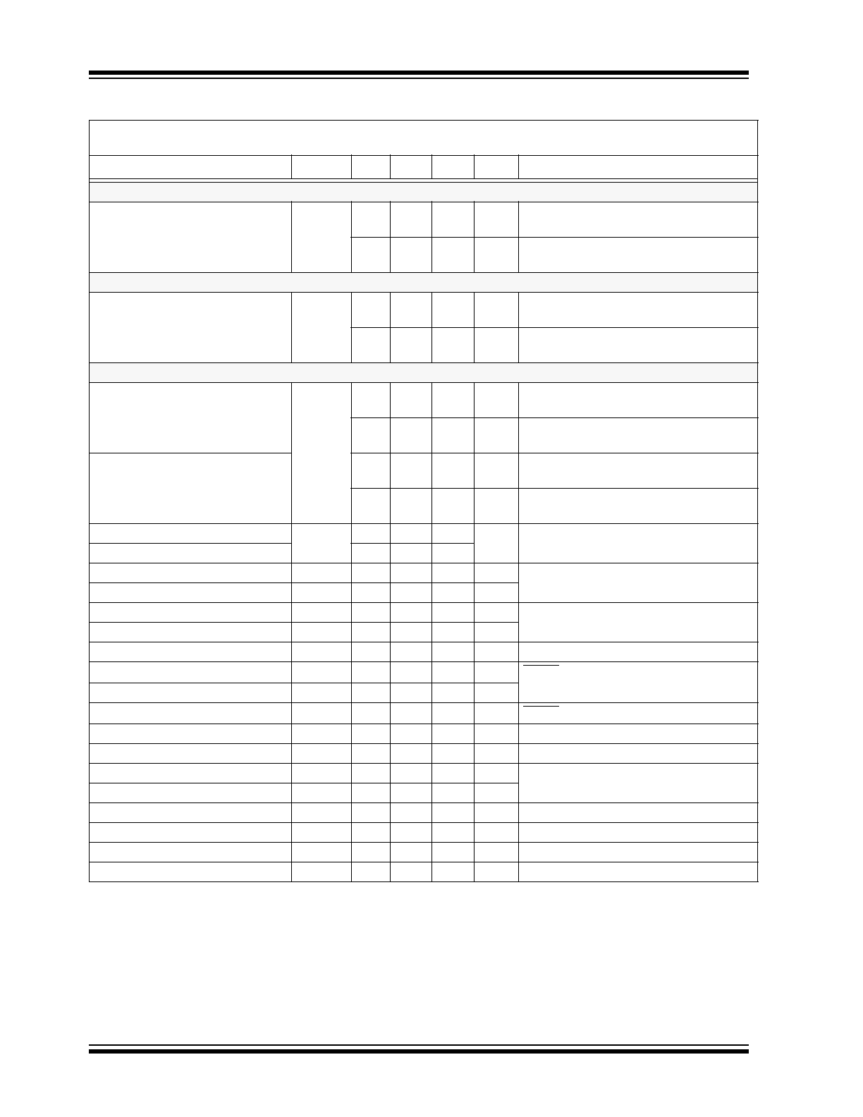
DC ELECTRICAL CHARACTERISTICS (CONTINUED)
Unless otherwise specified, V
DD
= 6.0V, V
SS
= -6.0V, V
LL
= 3.3V, T
AMB
= +25°C. Boldface specifications apply over
the full operating temperature range.
Parameters
Sym.
Min.
Typ.
Max.
Units
Conditions
Note 1:
Specification is obtained by characterization and is not 100% tested.
2:
Design guidance only.
2017 Microchip Technology Inc.
DS20005721A-page 5
HV2803/HV2903/HV2904
AC ELECTRICAL CHARACTERISTICS
Unless otherwise specified, V
DD
= 6.0V, V
SS
= -6.0V, V
LL
= 3.3V, T
AMB
= +25°C. Boldface specifications apply over
the full operating temperature range.
Parameters
Sym.
Min.
Typ.
Max.
Units
Conditions/Comments
Setup Time before LE/EN Rises
t
SD
25
—
—
ns
(
Note 1
)
Time Width of LE/EN t
WLE
12
—
—
ns
(
Note 1
)
Clock Delay Time to Data Out
t
DO
—
—
13.5
ns
Time Width of CLR
t
WCLR
55
—
—
ns
(
Note 1
)
Setup Time Data to Clock
t
SU
1.5
—
—
ns
(
Note 1
)
Hold Time Data from Clock
t
H
1.5
—
—
ns
(
Note 1
)
Clock Frequency
f
CLK
—
—
66
MHz
50% duty cycle, f
DIN
= (1/2)f
CLK
,
C
DOUT
= 20 pF (
Note 1
)
Clock Rise and Fall Times
t
R
, t
F
—
—
50
ns
Turn-On Time
t
ON
—
—
5
μs
V
SIG
= 5V, R
LOAD
= 550
(see
Figure 3-4
)
Turn-Off Time
t
OFF
—
—
5
Input Large-Signal Pulse Width
t
PW
—
—
2.5
μs
V
PULSE
= 0V to ±100V,
Measured at 90% amplitude
(see
Figure 3-5
) (
Note 1
)
Wake-up Time from Standby to
Digital Logic Normal Operation
t
WU
—
—
10
μs
Bank Switching mode (MODE = L)
—
—
10
μs
Individual Switching mode
(MODE = H) (
Note 1
)
Maximum V
SIG
Slew Rate
dv/dt
—
—
20
V/ns
(
Note 1
)
Analog Small-Signal Frequency
f
BWS
—
50
—
MHz
(
Note 1
)
Off Isolation
K
O
—
-57
-51
dB
f = 5.0 MHz,1.0 k
/15 pF load
(see
Figure 3-6
) (
Note 1
)
—
-70
-65
f = 5.0 MHz, 50
load
(see
Figure 3-6
) (
Note 1
)
Switch Crosstalk
K
CR
—
-70
-60
dB
f = 5.0 MHz, 50
load
(see
Figure 3-7
) (
Note 1
)
Off Capacitance SW to GND
C
SG(OFF)
—
9
—
pF
V
SIG
= 50 mV@1 MHz, no load
(
Note 1
)
On Capacitance SW to GND
C
SG(ON)
—
27
—
Output Voltage Spike at SWA,
SWB
+V
SPK
—
—
100
mV
R
LOAD
= 50
. (see
Figure 3-8
)
(
Note 1
)
-V
SPK
-150
—
—
Charge Injection
QC
—
200
—
pC
See
Figure 3-9
(
Note 1
)
Second Harmonic Distortion
HD2
—
-68
-60
dBc
V
SIG
= 1.5 V
PP
@ 5 MHz,
50Ω load (
Note 1
)
—
-65
-60
dBc
V
SIG
= 1.5 V
PP
@ 5 MHz,
1 k
/15 pF load (
Note 1
)
Note 1:
Specification is obtained by characterization and is not 100% tested.
TEMPERATURE SPECIFICATION
Parameters
Sym.
Min.
Typ.
Max.
Units
Conditions
Temperature Range
Operating Temperature Range
T
A
0
—
+70
°C
Storage Temperature Range
T
A
-65
—
+150
°C
Maximum Junction Temperature
T
J
—
—
+125
°C
Package Thermal Resistance
Thermal Resistance, 132-Ball TFBGA
JA
—
22
—
°C/W
HV2803/HV2903/HV2904
DS20005721A-page 6
2017 Microchip Technology Inc.
1.1
Logic Timing and Truth Table
Figure 1-1
shows the timing of the AC characteristic
parameters graphically.
FIGURE 1-1:
Logic Input Timing Diagram.
%
0
5
%
0
5
D
N+1
D
N
D
N-1
50%
50%
50%
50%
CLK
t
WLE
t
SD
t
H
t
SU
t
DO
50%
D
OUT
t
ON
t
OFF
V
OUT
(typ.)
CLR
50%
50%
t
WCLR
10%
90%
OFF
ON
V
LL
MODE
GND
LE/EN
D
IN
/AB
2017 Microchip Technology Inc.
DS20005721A-page 7
HV2803/HV2903/HV2904
TABLE 1-1:
TRUTH TABLE
(
1
,
2
,
3
,
4
,
5
,
6
)
STBY MODE D0 D1 ... D15 D16 ... D31 D
IN
/AB LE/EN CLR SW0 SW1 ...
SW15 SW16 ...
SW31
H
H
L
—
...
—
—
...
—
X
L
L
OFF
—
...
—
—
...
—
H
H
H —
—
—
—
X
L
L
ON
—
—
—
—
H
H
—
L
—
—
—
X
L
L
—
OFF
—
—
—
H
H
— H
—
—
—
X
L
L
—
ON
—
—
—
H
H
— —
—
—
—
X
L
L
—
—
—
—
—
H
H
— —
—
—
—
X
L
L
—
—
—
—
—
H
H
— —
L
—
—
X
L
L
—
—
OFF
—
—
H
H
— —
H
—
—
X
L
L
—
—
ON
—
—
H
H
— —
—
L
—
X
L
L
—
—
—
OFF
—
H
H
— —
—
H
—
X
L
L
—
—
—
ON
—
H
H
— —
—
—
—
X
L
L
—
—
—
—
—
H
H
— —
—
—
—
X
L
L
—
—
—
—
—
H
H
— —
—
—
L
X
L
L
—
—
—
—
OFF
H
H
— —
—
—
H
X
L
L
—
—
—
—
ON
H
H
X
X
X
X
X
X
X
X
H
L
HOLD PREVIOUS STATE
H
H
X
X
X
X
X
X
X
X
X
H
ALL SWITCHES OFF
H
L
X
X
X
X
X
X
X
L
H
X
EVEN SWITCHES OFF & ODD SWITCHES ON
H
L
X
X
X
X
X
X
X
H
H
X
EVEN SWITCHES ON & ODD SWITCHES OFF
H
L
X
X
X
X
X
X
X
X
L
X
ALL SWITCHES OFF
L
X
X
X
X
X
X
X
X
X
X
X
ALL SWITCHES OFF, STANBY STATE
Legend:
X = Don’t care; L = Low; H = High.
Note 1:
The 32 switches operate independently (when MODE = H).
2:
Serial data is clocked in on the L to H transition of the CLK (when MODE = H).
3:
All 32 switches go to a state retaining their latched condition at the rising edge of LE/EN. When LE/EN is
low, the shift registers’ data flows through the latch (when MODE = H).
4:
D
OUT
is high when data in Register 31 is high (when MODE = H).
5:
Shift register clocking has no effect on the switch states if LE/EN is high (when MODE = H).
6:
The CLR (clear) input overrides all the inputs (when MODE = H).
HV2803/HV2903/HV2904
DS20005721A-page 8
2017 Microchip Technology Inc.
2.0
PACKAGE PIN
CONFIGURATION AND
FUNCTION DESCRIPTION
This section details the pin designation for the 132-Ball
TFBGA package (
Figure 2-1
). The description of the
pins are listed in
Table 2-1
.
FIGURE 2-1:
132-Ball TFBGA Package – Top View.
10
11
12
13
A
B
C
D
E
F
G
H
P
J
K
L
M
14
N
D
OUT
CLK
GND
V
SS
SW9A
SW8A
SW7A
SW6A
V
SS
V
DD
V
LL
CLR
MODE
STBY
V
DD
V
DD
V
SS
V
DD
SW10A
SW5A
SW11A
SW4A
SW12A
SW3A
SW13A
SW2A
SW14A
SW1A
SW15A
SW0A
SW16A
SW31A
SW17A
SW30A
SW18A
SW29A
SW19A
SW28A
SW20A
V
DD
V
SS
V
SS
V
DD
SW27A
SW21A
V
DD
V
SS
SW22A
SW23A
SW24A
SW25A
V
SS
V
DD
SW26A
SW10B
SW11B
SW12B
SW13B
SW14B
SW15B
SW16B
SW17B
SW18B
SW19B
SW20B
SW21B
SW9B
SW8B
SW7B
SW6B
GND
GND
GND
GND
GND
GND
GND
GND
GND
GND
GND
GND
GND
GND
GND
GND
GND
GND
GND
GND
GND
GND
GND
GND
GND
GND
GND
GND
GND
GND
GND
GND
GND
GND
GND
GND
SW22B
SW23B
SW24B
SW25B
SW5B
SW4B
SW3B
SW2B
SW1B
SW0B
SW31B
SW30B
SW29B
SW28B
SW27B
SW26B
1
2
3
4
5
6
7
8
9
TOP VIEW
LE
EN
D
IN
AB
NC
R
GND
NC
R
GND
NC
R
GND
NC
R
GND
NC
R
GND
NC
R
GND
NC
R
GND
NC
R
GND
DGND
2017 Microchip Technology Inc.
DS20005721A-page 9
HV2803/HV2903/HV2904
TABLE 2-1:
PIN FUNCTION TABLE
Pin Number
Symbol
Description
HV2803
HV2903,
HV2904
A1
D
OUT
D
OUT
Data Out Logic Output
A2
V
LL
V
LL
Logic Supply Voltage
A3
SW10A
SW10A
Analog Switch 10 Terminal A
A4
SW11A
SW11A
Analog Switch 11 Terminal A
A5
SW12A
SW12A
Analog Switch 12 Terminal A
A6
SW13A
SW13A
Analog Switch 13 Terminal A
A7
SW14A
SW14A
Analog Switch 14 Terminal A
A8
SW15A
SW15A
Analog Switch 15 Terminal A
A9
SW16A
SW16A
Analog Switch 16 Terminal A
A10
SW17A
SW17A
Analog Switch 17 Terminal A
A11
SW18A
SW18A
Analog Switch 18 Terminal A
A12
SW19A
SW19A
Analog Switch 19 Terminal A
A13
SW20A
SW20A
Analog Switch 20 Terminal A
A14
SW21A
SW21A
Analog Switch 21 Terminal A
B1
CLK
CLK
Clock Logic Input for Shift Register
B2
CLR
CLR
Latch Clear Logic Input
B3
SW10B
SW10B
Analog Switch 10 Terminal B
B4
SW11B
SW11B
Analog Switch 11 Terminal B
B5
SW12B
SW12B
Analog Switch 12 Terminal B
B6
SW13B
SW13B
Analog Switch 13 Terminal B
B7
SW14B
SW14B
Analog Switch 14 Terminal B
B8
SW15B
SW15B
Analog Switch 15 Terminal B
B9
SW16B
SW16B
Analog Switch 16 Terminal B
B10
SW17B
SW17B
Analog Switch 17 Terminal B
B11
SW18B
SW18B
Analog Switch 18 Terminal B
B12
SW19B
SW19B
Analog Switch 19 Terminal B
B13
SW20B
SW20B
Analog Switch 20 Terminal B
B14
SW21B
SW21B
Analog Switch 21 Terminal B
C1
LE/EN
LE/EN
Latch Enable Logic Input, Low Active when in Individual Switching mode;
Enable Logic Input when in Bank Switching mode
C2
MODE
MODE
Logic Input to decide the Switching mode; L = Bank Switching,
H = Individual Switching
C13, C14
NC
R
GND
No Connect/Ground for Bleed Resistor
D1
D
IN
/AB
D
IN
/AB
Data in Logic Input when in Individual Switching mode; Logic Input to select
Even SWs Bank or Odd SWs Bank when in Bank Switching mode
D2
STBY
STBY
Logic Input for Standby State; L = Standby mode (default),
H = Normal Operation
D13, D14
V
DD
V
DD
Positive Supply Voltage
E1
DGND
DGND
Digital Ground
E2
V
DD
V
DD
Positive Supply Voltage
E5-E10
GND
GND
Ground
E13, E14
V
SS
V
SS
Negative Supply Voltage
HV2803/HV2903/HV2904
DS20005721A-page 10
2017 Microchip Technology Inc.
F1
V
SS
V
SS
Negative Supply Voltage
F2
V
DD
V
DD
Positive Supply Voltage
F5-F10
GND
GND
Ground
F13
SW22B
SW22B
Analog Switch 22 Terminal B
F14
SW22A
SW22A
Analog Switch 22 Terminal A
G1
SW9A
SW9A
Analog Switch 9 Terminal A
G2
SW9B
SW9B
Analog Switch 9 Terminal B
G5-G10
GND
GND
Ground
G13
SW23B
SW23B
Analog Switch 23 Terminal B
G14
SW23A
SW23A
Analog Switch 23 Terminal A
H1
SW8A
SW8A
Analog Switch 8 Terminal A
H2
SW8B
SW8B
Analog Switch 8 Terminal B
H5-H10
GND
GND
Ground
H13
SW24B
SW24B
Analog Switch 24 Terminal B
H14
SW24A
SW24A
Analog Switch 24 Terminal A
J1
SW7A
SW7A
Analog Switch 7 Terminal A
J2
SW7B
SW7B
Analog Switch 7 Terminal B
J5-J10
GND
GND
Ground
J13
SW25B
SW25B
Analog Switch 25 Terminal B
J14
SW25A
SW25A
Analog Switch 25 Terminal A
K1
SW6A
SW6A
Analog Switch 6 Terminal A
K2
SW6B
SW6B
Analog Switch 6 Terminal B
K5-K10
GND
GND
Ground
K13, K14
NC
R
GND
No Connect/Ground for Bleed Resistor
L1, L2
V
SS
V
SS
Negative Supply Voltage
L13, L14
V
SS
V
SS
Negative Supply Voltage
M1, M2
V
DD
V
DD
Positive Supply Voltage
M13, M14
V
DD
V
DD
Positive Supply Voltage
N1, N2
NC
R
GND
No Connect/Ground for Bleed Resistor
N3
SW5B
SW5B
Analog Switch 5 Terminal B
N4
SW4B
SW4B
Analog Switch 4 Terminal B
N5
SW3B
SW3B
Analog Switch 3 Terminal B
N6
SW2B
SW2B
Analog Switch 2 Terminal B
N7
SW1B
SW1B
Analog Switch 1 Terminal B
N8
SW0B
SW0B
Analog Switch 0 Terminal B
N9
SW31B
SW31B
Analog Switch 31 Terminal B
N10
SW30B
SW30B
Analog Switch 30 Terminal B
N11
SW29B
SW29B
Analog Switch 29 Terminal B
N12
SW28B
SW28B
Analog Switch 28 Terminal B
N13
SW27B
SW27B
Analog Switch 27 Terminal B
N14
SW26B
SW26B
Analog Switch 26 Terminal B
TABLE 2-1:
PIN FUNCTION TABLE (CONTINUED)
Pin Number
Symbol
Description
HV2803
HV2903,
HV2904