
2015 Microchip Technology Inc.
DS20005449A-page 1
HV2802/HV2902
Features
• 32-Channel SPST (Single-Pole, Single-Throw)
High-Voltage Analog Switch
• 3.3V or 5.0V CMOS Input Logic Level
• 20 MHz Data Shift Clock Frequency
• High-Voltage CMOS (HVCMOS) Technology for
High Performance
• Very Low Quiescent Power Dissipation (10 µA)
• Low Parasitic Capacitance
• DC to 50 MHz Analog Signal Frequency
• -60 dB Typical OFF-Isolation at 5.0 MHz
• CMOS Logic Circuitry for Low Power
• Excellent Noise Immunity
• Cascadable Serial Data Register with Latches
• Flexible Operating Supply Voltages
• Integrated Bleed Resistors on the Outputs
(HV2902 only)
Applications
• Medical Ultrasound Imaging
• Non-Destructive Testing (NDT) Metal Flaw
Detection
• Piezoelectric Transducer Drivers
• Inkjet Printer Heads
• Optical MEMS Modules
General Description
The HV2802 and HV2902 are low-charge injection,
32-channel, high-voltage analog switches intended for
use in applications requiring high-voltage switching
controlled by low-voltage control signals, such as
medical ultrasound imaging, driving piezoelectric
transducers and printers. The HV2902 has integrated
bleed resistors which eliminate voltage build-up on
capacitive loads such as piezoelectric transducers.
Input data are shifted into a 32-bit shift register that can
then be retained in a 32-bit latch. To reduce any
possible clock feedthrough noise, the latch enable bar
should be left high until all bits are clocked in. Data are
clocked in during the rising edge of the clock. Using the
HVCMOS technology, this device combines
high-voltage bilateral DMOS switches and low-power
CMOS logic to provide efficient control of high-voltage
analog signals.
The device is suitable for various combinations of
high-voltage supplies, e.g., V
PP
/V
NN
: +40V/-160V,
+100V/-100V and +160V/-40V.
Package Type
*
See
Section 2.0 “Package Pin Configurations and
Functions Description”
HV2802/HV2902
9x9x1.0 mm VFBGA*
Top View
13
12
11
10
9
8
7
6
5
4
3
2
1
A
B
C
D
E
F
G
H
J
K
L
M
N
Low Harmonic Distortion, 32-Channel SPST,
High-Voltage Analog Switch
HV2802/HV2902
DS20005449A-page 2
2015 Microchip Technology Inc.
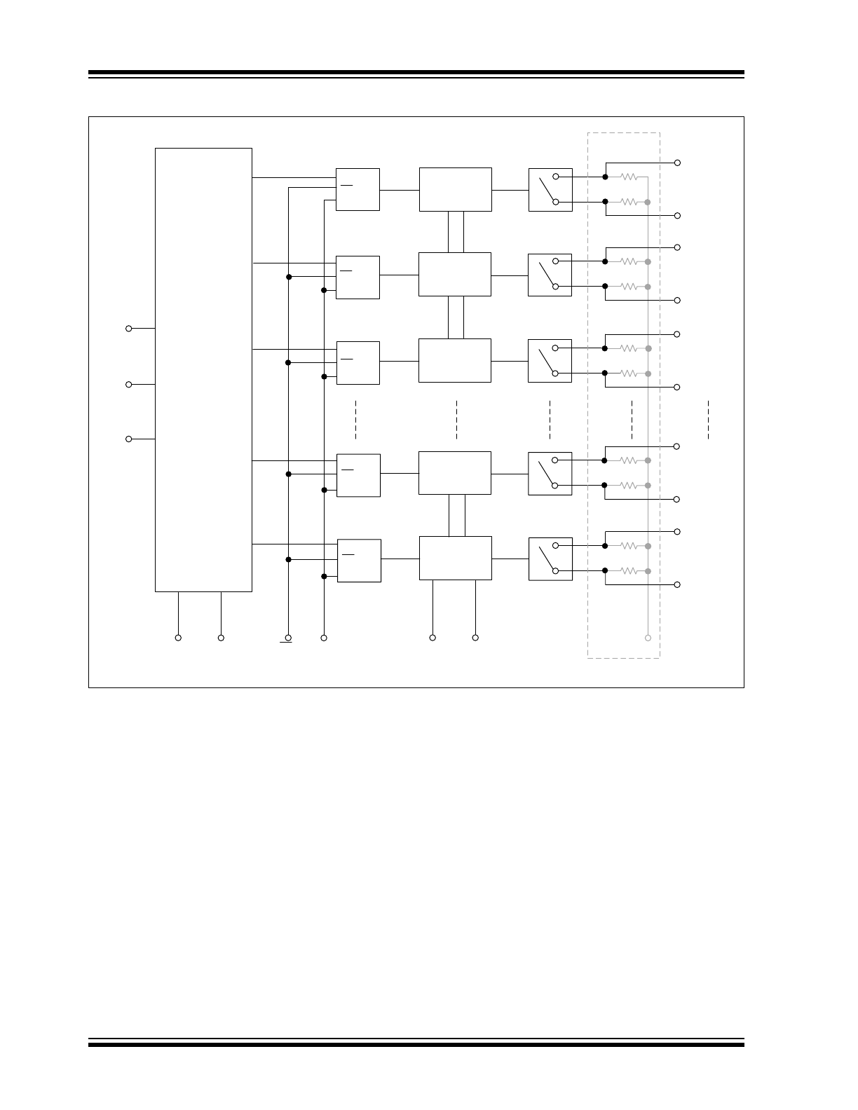
Block Diagram
Level
Shifters
V
PP
V
NN
Latches
CLR
LE
CLK
D
IN
GND
V
DD
Output
Switches
D
OUT
SW0A
SW0B
SW1A
SW1B
SW2A
SW2B
SW30A
SW30B
SW31A
SW31B
D
LE
CLR
32-Bit
Shift
Register
D
LE
CLR
D
LE
CLR
D
LE
CLR
D
LE
CLR
Bleed
Resistors
RGND
HV2902 only
2015 Microchip Technology Inc.
DS20005449A-page 3
HV2802/HV2902
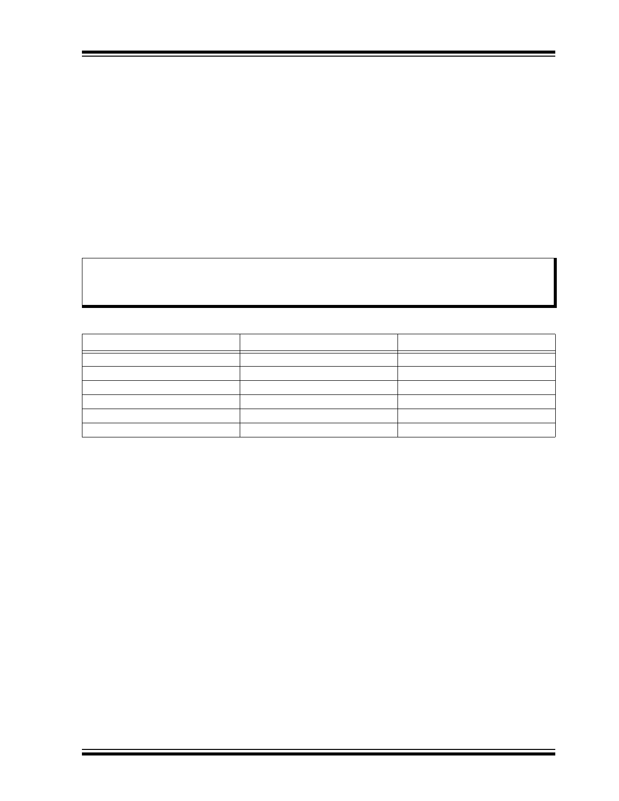
1.0
ELECTRICAL
CHARACTERISTICS
Absolute Maximum Ratings †
V
DD
Logic Supply Voltage .......................................................................................................................... -0.5V to +6.5V
V
PP
-V
NN
Differential Supply ......................................................................................................................................220V
V
PP
Positive Supply ...........................................................................................................................-0.5V to V
NN
+200V
V
NN
Negative Supply ................................................................................................................................ +0.5V to -200V
Logic Input Voltage..............................................................................................................................-0.5V to V
DD
+0.3V
Analog Signal Range .......................................................................................................................................V
NN
to V
PP
Peak Analog Signal Current/Channel ........................................................................................................................3.0A
Power Dissipation .................................................................................................................................................... 1.5W
† Notice:
Stresses above those listed under “Absolute Maximum Ratings” may cause permanent damage to the
device. This is a stress rating only and functional operation of the device at those or any other conditions above those
indicated in the operational listings of this specification is not implied. Exposure to maximum rating conditions for
extended periods may affect device reliability.
RECOMMENDED OPERATING CONDITIONS (
Note 1
—
3
)
Parameter
Symbol
Value
Logic Power Supply Voltage
V
DD
+3.0V to +5.5V
Positive Voltage Supply
V
PP
+40V to V
NN
+200V
Negative Voltage Supply
V
NN
-40V to -160V
High-Level Input Voltage
V
IH
0.9V
DD
to V
DD
Low-Level Input Voltage
V
IL
0V to 0.1V
DD
Analog Signal Voltage Peak-to-Peak
V
SIG
V
NN
+10V to V
PP
-10V
Note 1:
Power up/down sequence is arbitrary except GND must be powered-up first and powered-down last.
2:
V
SIG
must be V
NN
V
SIG
V
PP
or floating during power up/down transition.
3:
Rise and fall times of power supplies V
DD
, V
PP
, and V
NN
should not be less than 1.0 ms.
HV2802/HV2902
DS20005449A-page 4
2015 Microchip Technology Inc.
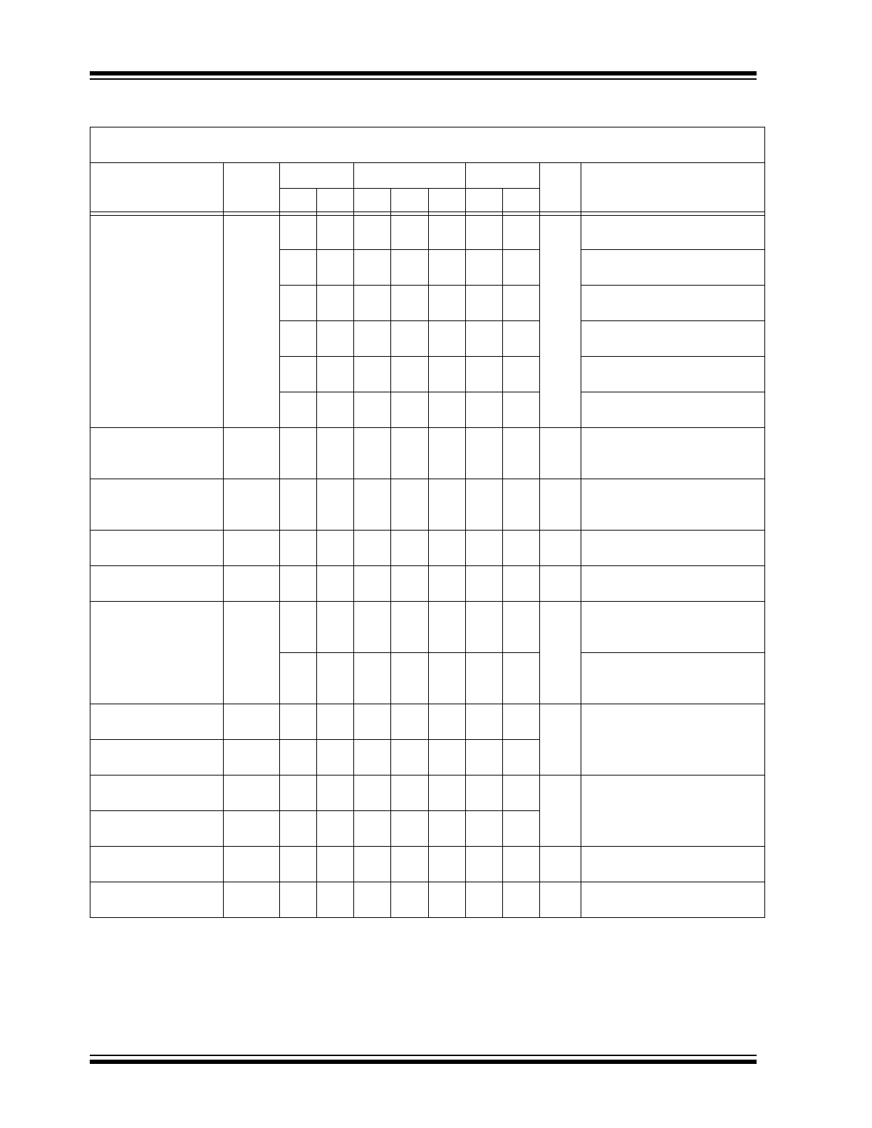
DC ELECTRICAL CHARACTERISTICS
Electrical Specifications:
Unless otherwise specified, V
DD
= 5.0V, V
PP
= +100V, V
NN
= -100V, Specification at 0°C
and 70°C based on characterization and not 100% tested.
Parameters
Symbol
0°C
+25°C
+70°C
Units
Conditions
Min. Max. Min. Typ. Max. Min. Max.
Small Signal Switch
ON-Resistance
R
ONS
—
30
—
26
38
—
48
I
SIG
= 5.0 mA,
V
PP
= +40V, V
NN
= -160V
—
25
—
22
27
—
32
I
SIG
= 200 mA,
V
PP
= +40V, V
NN
= -160V
—
25
—
22
27
—
30
I
SIG
= 5.0 mA,
V
PP
= +100V, V
NN
= -100V
—
18
—
18
24
—
27
I
SIG
= 200 mA,
V
PP
= +100V, V
NN
= -100V
—
23
—
20
25
—
30
I
SIG
= 5.0 mA,
V
PP
= +160V, V
NN
= -40V
—
22
—
16
25
—
27
I
SIG
= 200 mA,
V
PP
= +160V, V
NN
= -40V
Small Signal Switch
ON-Resistance
Matching
R
ONS
—
20
—
5
20
—
20
%
I
SIG
= 5.0 mA,
V
PP
= +100V, V
NN
= -100V
Large Signal Switch
ON-Resistance
(
Note 1
)
R
ONL
—
—
—
15
—
—
—
V
SIG
= V
PP
-10V, I
SIG
= 1A
Value of Output Bleed
Resistor
R
INT
—
—
20
35
50
—
—
k
Output switch to RGND
I
RINT
= 0.5 mA
Switch off Leakage
per Switch
I
SOL
—
5
—
1
10
—
15
µA
V
SIG
= V
PP
-10V, V
NN
+10V
Switch DC Offset
V
OS
—
300
—
100
300
—
300
mV
Switch OFF,
R
LOAD
= 100 k
for HV2802
No load for HV2902
—
500
—
100
500
—
500
Switch ON
R
LOAD
= 100 k
for HV2802
No load for HV2902
Quiescent V
PP
Supply
Current
I
PPQ
—
—
—
10
50
—
—
µA
All switches off
Quiescent V
NN
Supply
Current
I
NNQ
—
—
—
10
50
—
—
Quiescent V
PP
Supply
Current
I
PPQ
—
—
—
10
50
—
—
µA
All switches on,
I
SW
= 5.0 mA
Quiescent V
NN
Supply
Current
I
NNQ
—
—
—
10
50
—
—
Switch Output Peak
Current (
Note 1
)
I
SW
—
—
2
3
—
—
—
A
V
SIG
duty cycle < 0.1%
Output Switching
Frequency (
Note 1
)
f
SW
—
—
—
—
50
—
—
kHz Duty cycle = 50%
Note 1:
Specification is obtained by characterization and is not 100% tested.
2:
Design guidance only.
2015 Microchip Technology Inc.
DS20005449A-page 5
HV2802/HV2902
Average V
PP
Supply
Current
I
PP
—
14
—
—
14
—
14
mA
V
PP
= +40V, V
NN
= -160V
All output switches are turning
on and off at 50 kHz with no load
—
14
—
—
14
—
14
V
PP
= +100V, V
NN
= -100V
All output switches are turning
on and off at 50 kHz with no load
—
14
—
—
14
—
14
V
PP
= +160V, V
NN
= -40V
All output switches are turning
on and off at 50 kHz with no load
Average V
NN
Supply
Current
I
NN
—
14
—
—
14
—
14
mA
V
PP
= +40V, V
NN
= -160V
All output switches are turning
on and off at 50 kHz with no load
—
14
—
—
14
—
14
V
PP
= +100V, V
NN
= -100V
All output switches are turning
on and off at 50 kHz with no load
—
14
—
—
14
—
14
V
PP
= +160V, V
NN
= -40V
All output switches are turning
on and off at 50 kHz with no load
Average V
DD
Supply
Current
I
DD
—
8
—
—
8
—
8
mA
f
CLK
= 5.0 MHz, V
DD
= 5.0V
Quiescent V
DD
Supply Current
I
DDQ
—
10
—
—
10
—
10
µA
All logic inputs are static
Data Out Source
Current
I
SOR
0.45
—
0.45 0.70
—
0.40
—
mA
V
OUT
= V
DD
-0.7V
Data Out Sink Current
I
SINK
0.45
—
0.45 0.70
—
0.40
—
mA
V
OUT
= 0.7V
Logic Input
Capacitance (
Note 2
)
C
IN
—
10
—
—
10
—
10
pF
DC ELECTRICAL CHARACTERISTICS (CONTINUED)
Electrical Specifications:
Unless otherwise specified, V
DD
= 5.0V, V
PP
= +100V, V
NN
= -100V, Specification at 0°C
and 70°C based on characterization and not 100% tested.
Parameters
Symbol
0°C
+25°C
+70°C
Units
Conditions
Min. Max. Min. Typ. Max. Min. Max.
Note 1:
Specification is obtained by characterization and is not 100% tested.
2:
Design guidance only.
HV2802/HV2902
DS20005449A-page 6
2015 Microchip Technology Inc.
AC ELECTRICAL CHARACTERISTICS
Electrical Specifications
: Unless otherwise specified, V
DD
= 5.0V, V
PP
= +100V, V
NN
= -100V, Specification at 0°C and
70°C based on characterization and not 100% tested.
Parameters
Symbol
0°C
+25°C
+70°C
Units
Conditions
Min. Max. Min. Typ. Max. Min. Max.
Set Up Time Before LE Rises
(
Note 1
)
t
SD
25
—
25
—
—
25
—
ns
Time Width of LE (
Note 1
)
t
WLE
56
—
56
—
—
56
—
ns
V
DD
= 3.0V
12
—
12
—
—
12
—
V
DD
= 5.0V
Clock Delay Time to Data Out
(
Note 1
)
t
DO
8
40
8
19
40
8
40
ns
V
DD
= 3.0V
8
30
8
15
30
8
30
V
DD
= 5.0V
Time Width of CLR (
Note 1
)
t
WCLR
55
—
55
—
—
55
—
ns
Set Up Time Data to Clock
(
Note 1
)
t
SU
21
—
21
—
—
21
—
ns
V
DD
= 3.0V
7
—
7
—
—
7
—
V
DD
= 5.0V
Hold Time Data from Clock
(
Note 1
)
t
H
5
—
5
—
—
5
—
ns
V
DD
= 3.0V
7
—
7
—
—
7
—
V
DD
= 5.0V
Clock Frequency
f
CLK
—
8
—
—
8
—
8
MHz V
DD
= 3.0V
—
20
—
—
20
—
20
V
DD
= 5.0V
Clock Rise and Fall Times
t
R
, t
F
—
50
—
—
50
—
50
ns
Turn ON Time
t
ON
—
5
—
—
5
—
5
µs
V
SIG
= V
PP
-10V,
R
LOAD
= 10 k
Turn OFF Time
t
OFF
—
5
—
—
5
—
5
Maximum V
SIG
Slew Rate
(
Note 1
)
dv/dt
—
—
—
—
20
—
—
V/ns V
PP
= +40V, V
NN
= -160V
—
—
—
—
20
—
—
V
PP
= +100V, V
NN
= -100V
—
—
—
—
20
—
—
V
PP
= +160V, V
NN
= -40V
OFF Isolation (
Note 1
)
K
O
—
—
—
-33
-30
—
—
dB
f = 5.0 MHz,
1.0 k
ǁ
15 pF load
—
—
—
-60
-58
—
—
f = 5.0 MHz,
50
load
Switch Crosstalk (
Note 1
)
K
CR
—
—
—
-70
-60
—
—
dB
f = 5.0 MHz,
50
load
Output Switch Isolation Diode
Current (
Note 1
)
I
ID
—
—
—
—
300
—
—
mA
300 ns pulse width,
2.0% duty cycle
Off Capacitance SW to GND
(
Note 1
)
C
SG(OFF)
—
—
—
10
15
—
—
pF
0V, f = 1.0 MHz
On Capacitance SW to GND
(
Note 1
)
C
SG(ON)
—
—
—
13
18
—
—
Output Voltage Spike SWA,
SWB (
Note 1
)
+V
SPK
—
—
—
—
+150
—
—
mV
V
PP
= +40V, V
NN
= -160V
R
LOAD
= 50
-V
SPK
—
—
-150
—
—
—
—
+V
SPK
—
—
—
—
+150
—
—
V
PP
= +100V, V
NN
= -100V
R
LOAD
= 50
-V
SPK
—
—
-150
—
—
—
—
+V
SPK
—
—
—
—
+150
—
—
V
PP
= +160V, V
NN
= -40V
R
LOAD
= 50
-V
SPK
—
—
-150
—
—
—
—
Charge Injection
(per switch) (
Note 1
)
QC
—
—
—
820
—
—
—
pC
V
PP
= +40V, V
NN
= -160V
—
—
—
600
—
—
—
V
PP
= +100V, V
NN
= -100V
—
—
—
350
—
—
—
V
PP
= +160V, V
NN
= -40V
Note 1:
Specification is obtained by characterization and is not 100% tested.
2015 Microchip Technology Inc.
DS20005449A-page 7
HV2802/HV2902
TEMPERATURE SPECIFICATIONS
Parameters
Sym.
Min.
Typ.
Max.
Units
Conditions
Temperature Ranges
Operating Temperature
T
A
0
—
+70
°C
Storage Temperature
T
A
-65
—
+150
°C
Package Thermal Resistance
Thermal Resistance, 78-Ball VFBGA
JA
—
32.2
—
°C/W
HV2802/HV2902
DS20005449A-page 8
2015 Microchip Technology Inc.
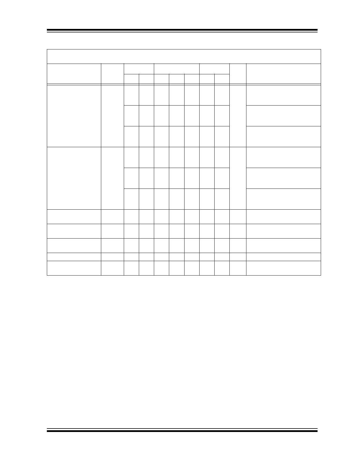
1.1
Logic Timing and Truth Table
FIGURE 1-1:
Logic Timing Waveforms.
TABLE 1-1:
TRUTH TABLE (
Notes 1
—
6
)
D0
D1
•••
D15
D16
•••
D31
LE
CLR
SW0
SW1
•••
SW15 SW16
•••
SW31
L
—
•••
—
—
•••
—
L
L
OFF
—
•••
—
—
•••
—
H
—
—
—
—
L
L
ON
—
—
—
—
—
L
—
—
—
L
L
—
OFF
—
—
—
—
H
—
—
—
L
L
—
ON
—
—
—
—
—
—
—
—
L
L
—
—
—
—
—
—
—
—
—
—
L
L
—
—
—
—
—
—
—
L
—
—
L
L
—
—
OFF
—
—
—
—
H
—
—
L
L
—
—
ON
—
—
—
—
—
L
—
L
L
—
—
—
OFF
—
—
—
—
H
—
L
L
—
—
—
ON
—
—
—
—
—
—
L
L
—
—
—
—
—
—
—
—
—
—
L
L
—
—
—
—
—
—
—
—
—
—
L
L
—
—
—
—
—
—
—
—
—
—
L
L
—
—
—
—
—
—
—
—
—
L
L
L
—
—
—
—
OFF
—
—
—
—
H
L
L
—
—
—
—
ON
X
X
X
X
X
X
X
H
L
HOLD PREVIOUS STATE
X
X
X
X
X
X
X
X
H
ALL SWITCHES OFF
Legend:
X = Do not care; L = Low; H = High.
Note 1:
The 32 switches operate independently.
2:
Serial data is clocked in on the L to H transition of the CLK.
3:
All 32 switches go to a state retaining their latched condition at the rising edge of LE. When LE is low, the
shift register’s data flow through the latch.
4:
D
OUT
is high when data in register 31 is high.
5:
Shift register’s clocking has no effect on the switch states if LE is high.
6:
The CLR clear input overrides all other inputs.
50%
D
N
D
N-1
D
N+1
50%
50%
50%
50%
50%
50%
50%
10%
50%
10%
DATA
IN
LE
CLOCK
DATA
OUT
OFF
ON
CLR
V
OUT
(typical)
t
WCL
t
OFF
t
WLE
t
SU
t
ON
t
DO
t
h
t
SD
50%
2015 Microchip Technology Inc.
DS20005449A-page 9
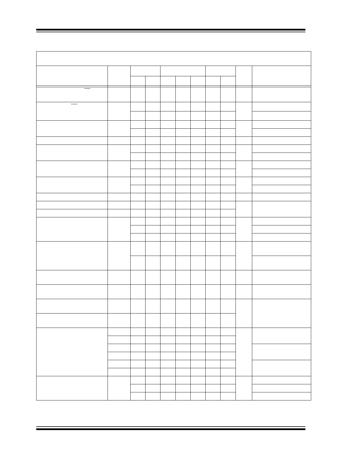
HV2802/HV2902
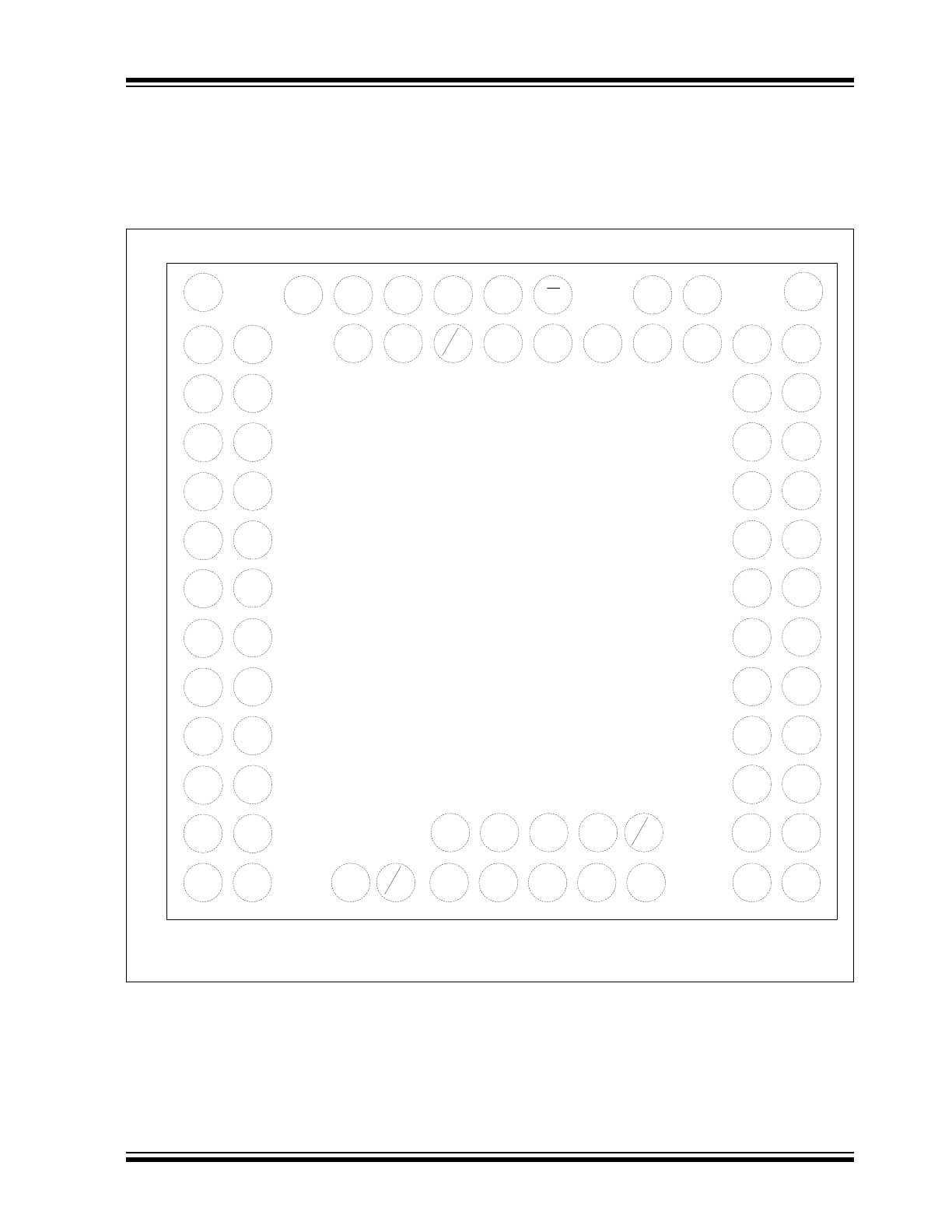
2.0
PACKAGE PIN CONFIGURATIONS
AND FUNCTIONS DESCRIPTION
This section details the pin designation for the 78-Ball
VFBGA package (
Figure 2-1
). The descriptions of the
pins are listed in
Table 2-1
.
FIGURE 2-1:
78-Ball VFBGA Package - Top View.
1
2
3
4
5
6
7
8
9
10
11
12
13
A
B
C
D
E
F
G
H
J
K
L
M
N
SW2B
SW3A
SW4A
SW5A
SW6A
SW7A
SW8A
SW9A
SW10A
SW11A
SW12A
SW13A
SW12B
SW8B
SW24B
SW25B
SW26A
SW27A
SW26B
SW28A
SW29A
SW29B
SW28B
SW27B
SW30A
SW30B
SW31B
SW31A
CLR
CLK
D
IN
SW1A
SW0A
V
DD
LE
GND
D
OUT
SW0B
SW1B
SW11B
SW10B
SW9B
SW2A
SW3B
SW7B
SW6B
SW5B
SW4B
SW25A
SW24A
SW23B
SW22B
SW18B
V
NN
V
PP
SW17B
SW16B
SW15B
SW14B
SW13B
V
NN
V
PP
SW14A
SW15A
SW16A
SW17A
SW18A
SW19A
SW19B
SW20A
SW21A
SW20B
SW22A
SW21B
SW23A
NC
RGND
NC
RGND
NC
RGND
Note:
On pins B6, M10 and N5 the NC pin is available for
HV2802
only, while RGND pin is available for HV2902.
HV2802/HV2902
DS20005449A-page 10
2015 Microchip Technology Inc.
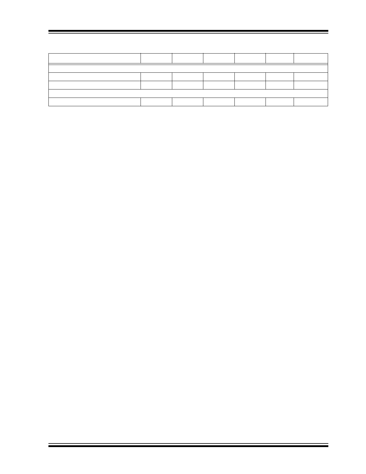
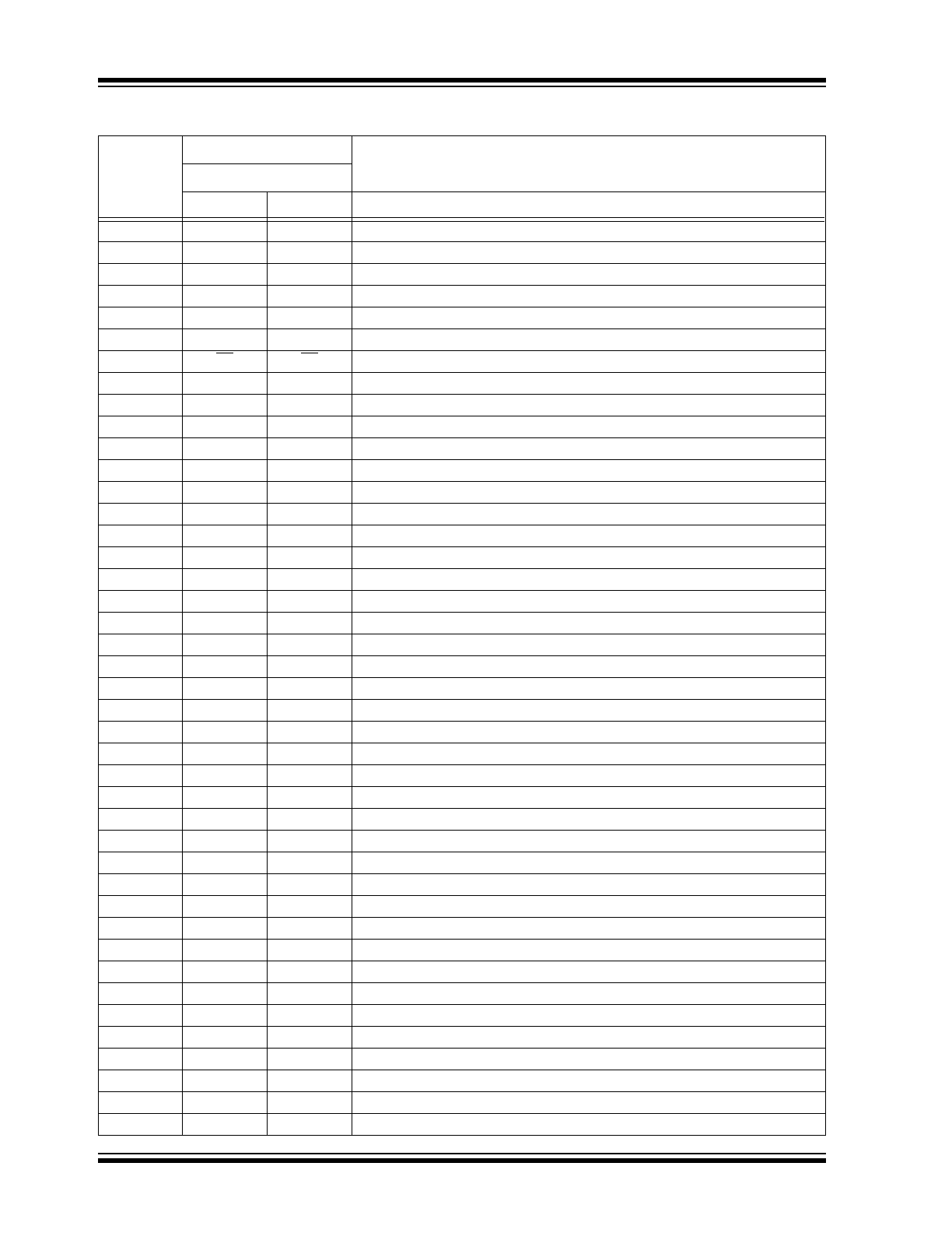
TABLE 2-1:
PIN FUNCTION TABLE
Pin
Number
Symbol
Description
9x9x1.0 VFBGA
HV2802
HV2902
A1
SW2B
SW2B
Analog switch 2 terminal B
A3
SW1B
SW1B
Analog switch 1 terminal B
A4
SW0B
SW0B
Analog switch 0 terminal B
A5
D
OUT
D
OUT
Data out logic output
A6
GND
GND
Ground
A7
V
DD
V
DD
Logic supply voltage
A8
LE
LE
Latch enable logic input, low active
A10
SW31A
SW31A
Analog switch 31 terminal A
A11
SW30A
SW30A
Analog switch 30 terminal A
A13
SW29B
SW29B
Analog switch 29 terminal B
B1
SW3A
SW3A
Analog switch 3 terminal A
B2
SW2A
SW2A
Analog switch 2 terminal A
B4
SW1A
SW1A
Analog switch 1 terminal A
B5
SW0A
SW0A
Analog switch 0 terminal A
B6
NC
RGND
No connect / Ground for bleed resistor
B7
D
IN
D
IN
Data in logic input
B8
CLK
CLK
Clock logic input for shift register
B9
CLR
CLR
Latch clear logic input
B10
SW31B
SW31B
Analog switch 31 terminal B
B11
SW30B
SW30B
Analog switch 30 terminal B
B12
SW28B
SW28B
Analog switch 28 terminal B
B13
SW29A
SW29A
Analog switch 29 terminal A
C1
SW4A
SW4A
Analog switch 4 terminal A
C2
SW3B
SW3B
Analog switch 3 terminal B
C12
SW27B
SW27B
Analog switch 27 terminal B
C13
SW28A
SW28A
Analog switch 28 terminal A
D1
SW5A
SW5A
Analog switch 5 terminal A
D2
SW4B
SW4B
Analog switch 4 terminal B
D12
SW26B
SW26B
Analog switch 26 terminal B
D13
SW27A
SW27A
Analog switch 27 terminal A
E1
SW6A
SW6A
Analog switch 6 terminal A
E2
SW5B
SW5B
Analog switch 5 terminal B
E12
SW25B
SW25B
Analog switch 25 terminal B
E13
SW26A
SW26A
Analog switch 26 terminal A
F1
SW7A
SW7A
Analog switch 7 terminal A
F2
SW6B
SW6B
Analog switch 6 terminal B
F12
SW24B
SW24B
Analog switch 24 terminal B
F13
SW25A
SW25A
Analog switch 25 terminal A
G1
SW8A
SW8A
Analog switch 8 terminal A
G2
SW7B
SW7B
Analog switch 7 terminal B
G12
SW23B
SW23B
Analog switch 23 terminal B
G13
SW24A
SW24A
Analog switch 24 terminal A