
2016 Microchip Technology Inc.
DS20005628A-page 1
HT0740
Features
• ±400V Input to Output Isolation
• Low Input Logic Current, 500 µA (Maximum)
• No External Voltage Supply Required
• Floating Isolated Output Drivers
• 5V Logic Compatible
Applications
• Telecommunications
• Modems
• Solid State Relays
• High-side Switches
• High-end Audio Switches
• Avionics
• Automatic Test Equipment
General Description
The HT0740 is a single-channel high-voltage low input
current isolated driver that uses the HVCMOS
®
technology. It is designed to drive discrete MOSFETs
configured as high-side switches up to 400V. The
HT0740 generates an independent DC-isolated
voltage across +V
OUT
and –V
OUT
when the logic input
is at a logic high. The HT0740 does not require any
external power supplies. The internal supply voltage is
provided by the logic input when it is in high state.
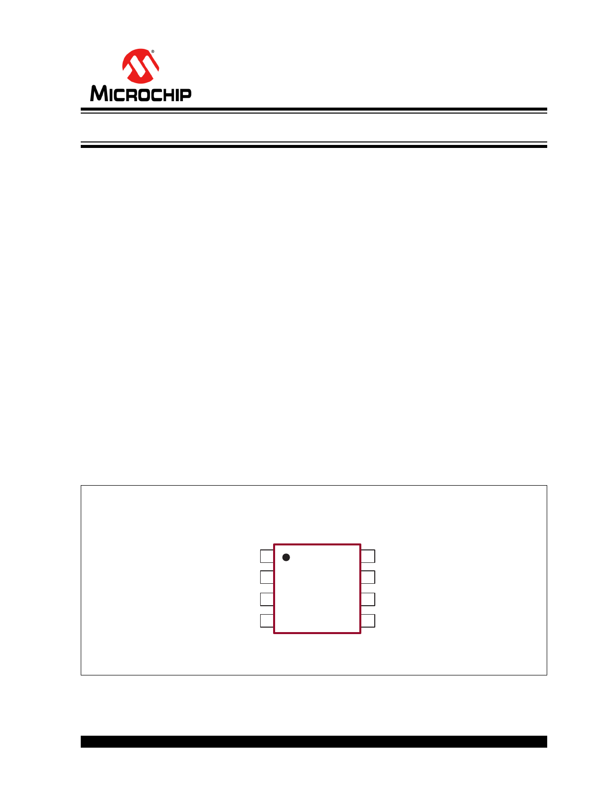
Package Type
8-lead SOIC
(Top view)
VIN
NC
-VOUT
+VOUT
1
2
3
4
8
7
6
5
NC
GND
NC
NC
See
Table 2-1
for pin information.
High-Voltage Isolated MOSFET Driver
V
ISO
R = 158kΩ ± 47%
Logic
&
Internal
Clock
Driver
+
VOUT
-
Isolation Barrier
10R
R
R
4
3
1
7
VIN
GND
HT0740
DS20005628A-page 2
2016 Microchip Technology Inc.
Functional Block Diagram
2016 Microchip Technology Inc.
DS20005628A-page 3
HT0740
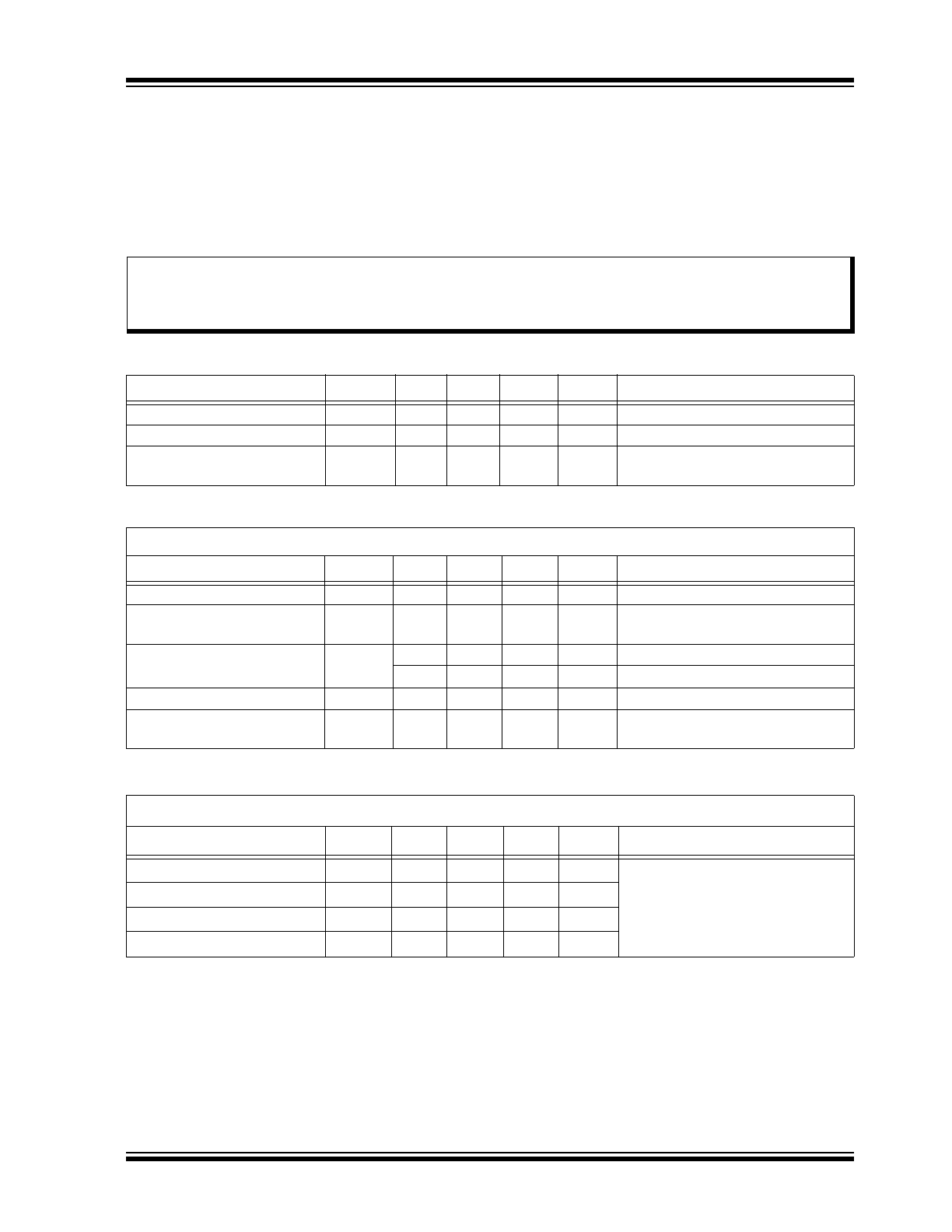
1.0
ELECTRICAL CHARACTERISTICS
Absolute Maximum Ratings†
Input to Output Isolation Voltage, V
ISO
................................................................................................................. ±400V
Logic Input Voltage, V
IN
..............................................................................................................................–0.5V to +7V
Operating Ambient Temperature, T
A
......................................................................................................–40°C to +85°C
Storage Temperature, T
S
......................................................................................................................–55°C to +150°C
† Notice: Stresses above those listed under “Absolute Maximum Ratings” may cause permanent damage to the
device. This is a stress rating only, and functional operation of the device at those or any other conditions above those
indicated in the operational sections of this specification is not intended. Exposure to maximum rating conditions for
extended periods may affect device reliability.
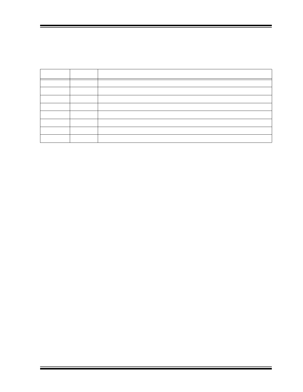
RECOMMENDED OPERATING CONDITIONS
Parameter
Sym.
Min.
Typ.
Max.
Unit
Conditions
Logic Input High Voltage
V
IH
3.15
—
5.5
V
Logic Input Low Voltage
V
IL
0
—
0.5
V
Operating Ambient
Temperature
T
A
–40
—
+85
°C
DC ELECTRICAL CHARACTERISTICS
Electrical Specifications: T
A
= 25°C unless otherwise indicated.
Parameter
Sym.
Min.
Typ.
Max.
Unit
Conditions
Logic High Input Current
I
H
—
—
500
µA
V
IN
= 5V
Logic Low Input Current
(Quiescent)
I
L
—
—
10
µA
V
IN
= 0.5V
Output Voltage Across Output
Terminals
V
OUT
4.5
—
—
V
V
IN
= 3.15V, no load
8.5
—
—
V
V
IN
= 4.5V, no load
Input Voltage for Zero Output
V
IN
—
—
0.8
V
No load
Input to Output Isolation
Voltage
V
ISO
±400
—
—
V
AC ELECTRICAL CHARACTERISTICS
Electrical Specifications: T
A
= 25°C unless otherwise indicated.
Parameter
Sym.
Min.
Typ.
Max.
Unit
Conditions
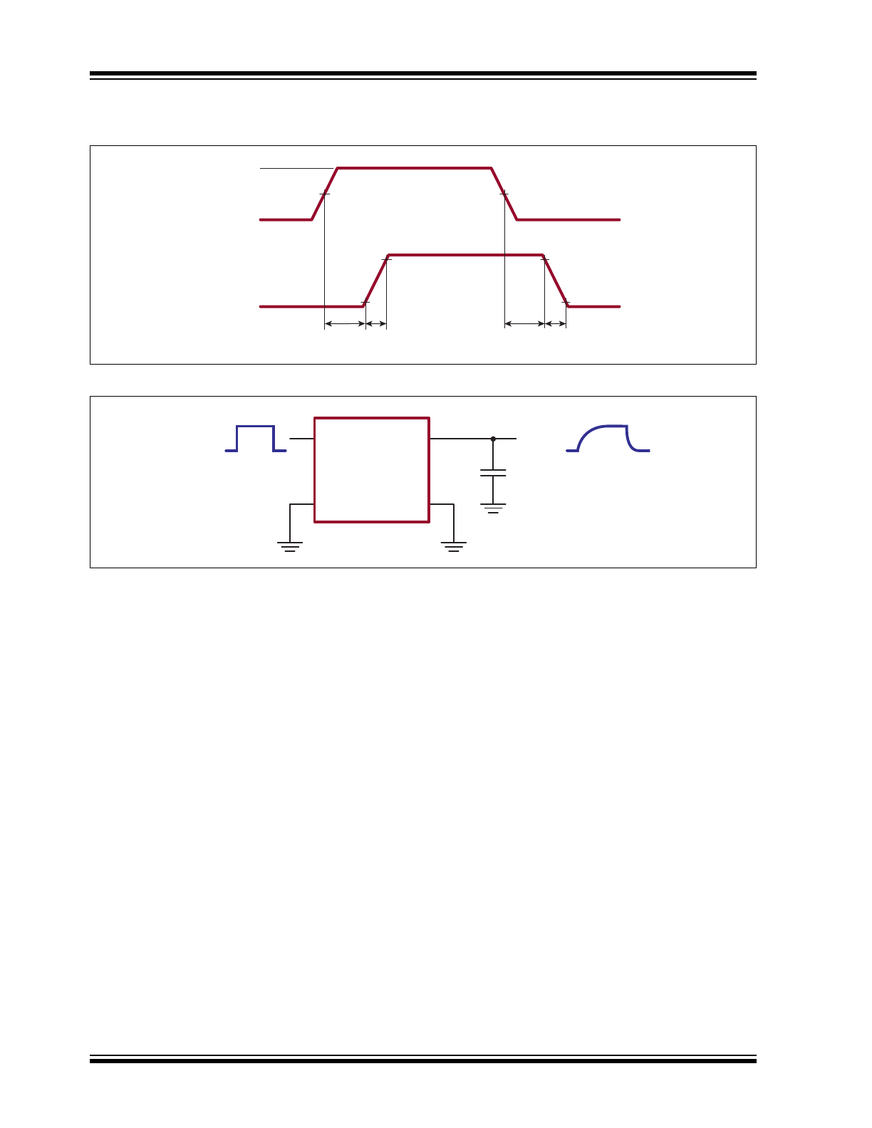
Turn-on Delay Time
t
d(ON)
—
—
50
µs
See
Figure 3-1
and
Figure 3-2
.
C
L
= 600 pF, T
A
= 25 °C
Rise Time
t
r
—
—
650
µs
Turn-off Delay Time
t
d(OFF)
—
—
150
µs
Fall Time
t
f
—
—
3
ms
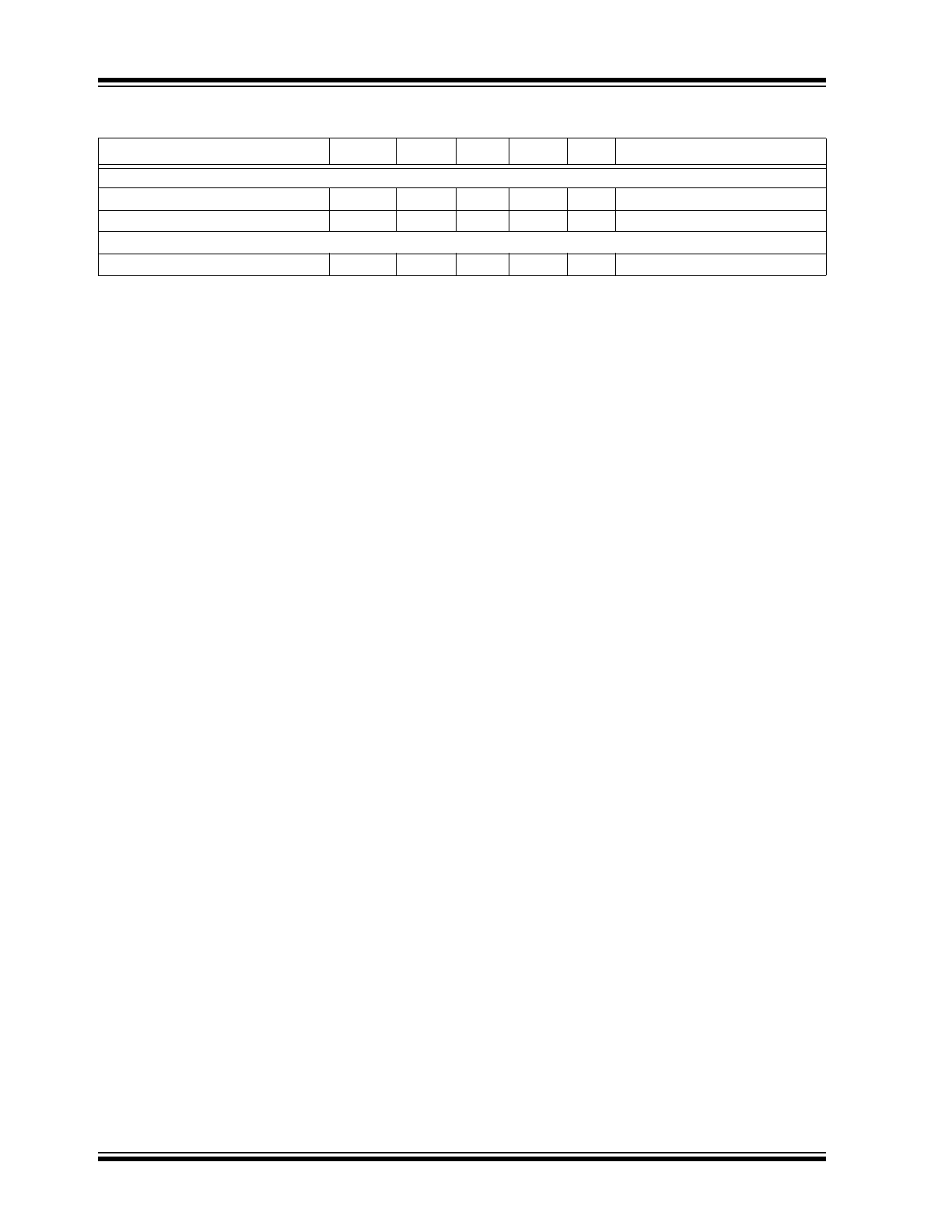
TEMPERATURE SPECIFICATIONS
Parameter
Sym.
Min.
Typ.
Max.
Unit
Conditions
TEMPERATURE RANGE
Operating Ambient Temperature
T
A
–40
—
+85
°C
Storage Temperature
T
S
–55
—
+150
°C
PACKAGE THERMAL RESISTANCE
8-lead SOIC
JA
—
101
—
°C/W
HT0740
DS20005628A-page 4
2016 Microchip Technology Inc.
2016 Microchip Technology Inc.
DS20005628A-page 5
HT0740
2.0
PIN DESCRIPTION
The details on the pins of HT0740 are listed on
Table 2-1
. Refer to
Package Type
for the location of
pins.
TABLE 2-1:
PIN FUNCTION TABLE
Pin Number
Pin Name
Description
1
VIN
Logic input
2
NC
No connect
3
–VOUT
Negative output
4
+VOUT
Positive output
5
NC
No connect
6
NC
No connect
7
GND
Ground
8
NC
No connect
HT0740
DS20005628A-page 6
2016 Microchip Technology Inc.
3.0
FUNCTIONAL DESCRIPTION
90%
10%
50%
50%
90%
10%
4.5V
0V
V
OUT
t
d(ON)
t
r
t
d(OFF)
t
f
V
IN
FIGURE 3-1:
Timing Waveforms.
HT0740
1
7
VIN
GND
+
VOUT
-
C
L
= 600pF
4
3
V
OUT
4.5V
0V
FIGURE 3-2:
Test Circuit.
2016 Microchip Technology Inc.
DS20005628A-page 7
HT0740
4.0
PACKAGING INFORMATION
4.1
Package Marking Information
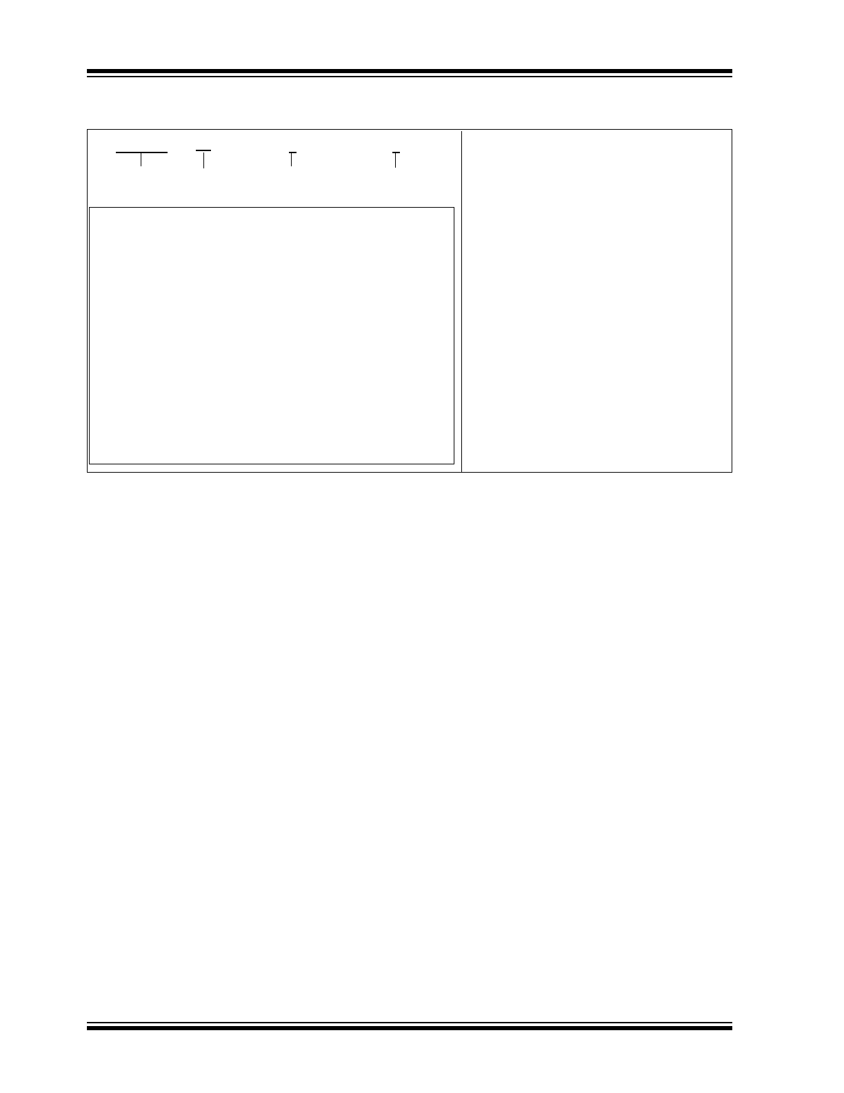
Legend: XX...X
Product Code or Customer-specific information
Y
Year code (last digit of calendar year)
YY
Year code (last 2 digits of calendar year)
WW
Week code (week of January 1 is week ‘01’)
NNN
Alphanumeric traceability code
Pb-free JEDEC
®
designator for Matte Tin (Sn)
*
This package is Pb-free. The Pb-free JEDEC designator ( )
can be found on the outer packaging for this package.
Note:
In the event the full Microchip part number cannot be marked on one line, it will
be carried over to the next line, thus limiting the number of available
characters for product code or customer-specific information. Package may or
not include the corporate logo.
3
e
3
e
8-lead SOIC
Example
NNN
XXXXXXXX
YYWW
e3
789
HT0740LG
1620
e3
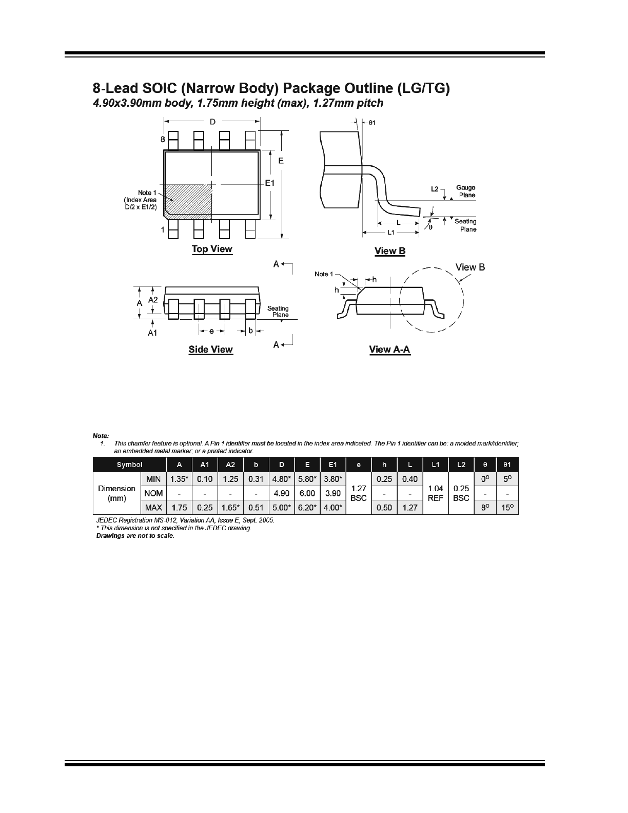
Note: For the most current package drawings, see the Microchip Packaging Specification at www.microchip.com/packaging.
HT0740
DS20005628A-page 8
2016 Microchip Technology Inc.

2016 Microchip Technology Inc.
DS20005628A-page 9
HT0740
APPENDIX A: REVISION HISTORY
Revision A (October 2016)
• Converted Supertex Doc# DSFP-HT0740 to
Microchip DS20005628A
• Changed the packaging quantity of the 8-lead
SOIC LG from 2500/Reel to 3300/Reel
• Made minor text changes throughout the docu-
ment
HT0740
DS20005628A-page 10
2016 Microchip Technology Inc.
PRODUCT IDENTIFICATION SYSTEM
To order or obtain information, e.g., on pricing or delivery, contact your local Microchip representative or sales office
.
Example:
a)
HT0740LG-G: High-Voltage Isolated MOSFET
Driver, 8-lead SOIC Package,
3300/Reel
PART NO.
Device
Device:
HT0740 =
High-Voltage Isolated MOSFET
Driver
Package:
LG
=
8-lead SOIC
Environmental:
G
=
Lead (Pb)-free/RoHS-compliant Package
Media Type:
(blank)
=
3300/Reel for an LG Package
XX
Package
-
X - X
Environmental Media Type
Options