
2016 Microchip Technology Inc.
DS20005598A-page 1
PL130-07
Features
• LVCMOS Output
• Selectable Drive Capability
- Drive 15 pF or 30 pF Output Load
• Single AC-Coupled Input (Min. 100 mV Swing)
• Accepts LVCMOS or Sine Wave Inputs
• Input Range from 10 MHz to 200 MHz
• OE High (PL130-07) or OE Low (PL130-07A)
Enable
• 2.5V to 3.3V Operation
• Available in 8-Pin SOIC, 8-Pin TSSOP and 3 mm
x 3 mm 16-Pin QFN
General Description
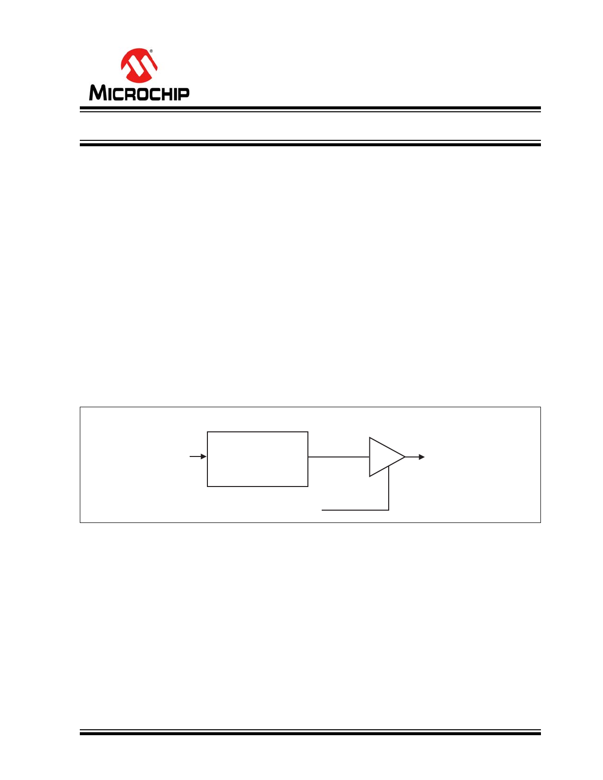
The PL130-07 is a low cost, high performance, high
speed, buffer that reproduces any input frequency from
10 MHz to 200 MHz. It provides an LVCMOS output
with 15 pF output load drive capability. Any input signal
with at least 100 mV swing can be used as reference
signal. This chip is ideal for conversion from sine wave
to LVCMOS.
Block Diagram
PL130-07
INPUT
AMPLIFIER
CLK_IN
CLK_OUT
OE
High Speed Translator Buffer to LVCMOS

PL130-07
DS20005598A-page 2
2016 Microchip Technology Inc.
1.0
ELECTRICAL CHARACTERISTICS
Absolute Maximum Ratings †
Supply Voltage (V
DD
) ...............................................................................................................................................+4.6V
Input Voltage (DC).............................................................................................................................–0.5V to V
DD
+ 0.5V
Output Voltage (DC) ..........................................................................................................................–0.5V to V
DD
+ 0.5V
HBM ESD Rating........................................................................................................................................................2 kV
† Notice: Stresses above those listed under “Absolute Maximum Ratings” may cause permanent damage to the device.
This is a stress rating only and functional operation of the device at those or any other conditions above those indicated
in the operational sections of this specification is not intended. Exposure to maximum rating conditions for extended
periods may affect device reliability.
2016 Microchip Technology Inc.
DS20005598A-page 3
PL130-07
TABLE 1-1:
AC ELECTRICAL CHARACTERISTICS
Parameters
Sym.
Min.
Typ.
Max.
Units
Conditions
Input Frequency
—
10
—
200
MHz
—
Input Signal Swing
—
100
—
—
mV
CLK_IN Input
Output Frequency
—
10
—
200
MHz
—
TABLE 1-2:
CMOS OUTPUT ELECTRICAL CHARACTERISTICS
Parameters
Sym.
Min.
Typ.
Max.
Units
Conditions
Output High Voltage
V
OH
2.4
—
—
V
I
OH
= 12 mA
Output Low Voltage
V
OL
—
—
0.4
V
I
OL
= 12 mA
Output High Voltage at CMOS Level
V
OHC
V
DD
–
0.4
—
—
V
I
OH
= –4 mA
Output Drive Current
—
36
51
—
mA
At TTL Level (High Drive,
Note 1
)
12
17
—
mA
At TTL Level (Standard Drive)
Quiescent Supply Current
I
DD
—
5.9
—
mA
No input signal, V
DD
= 2.5V
—
12.7
—
mA
No input signal, V
DD
= 3.3V
Note 1:
High Drive CMOS is selectable through DRIV_SEL selector input on pin 8(SOIC) or 13(QFN).
TABLE 1-3:
CMOS SWITCHING CHARACTERISTICS
Parameters
Sym.
Min.
Typ.
Max.
Units
Conditions
Output Clock Rise/Fall Time
t
r
/t
f
—
1.15
—
ns
0.8V ~ 2.0V with 10 pF load
—
3.7
—
ns
0.8V ~ 3.0V with 15 pF load
Output Clock Rise/Fall Time (High
Drive,
Note 1
)
t
r
/t
f
—
0.5
—
ns
0.8V ~ 2.0V with 10 pF load
—
1.5
—
ns
0.8V ~ 3.0V with 15 pF load
Note 1:
High Drive CMOS is selectable through DRIV_SEL selector input on pin 8(SOIC) or 13(QFN).

PL130-07
DS20005598A-page 4
2016 Microchip Technology Inc.
TEMPERATURE SPECIFICATIONS (
Note 1
)
Parameters
Sym.
Min.
Typ.
Max.
Units
Conditions
Temperature Ranges
Storage Temperature Range
T
S
–65
—
+150
°C
—
Ambient Operating Temperature
T
A
–40
—
+85
°C
Note 2
Junction Temperature
T
J
—
—
+125
°C
—
Lead Temperature
—
—
—
+260
°C
Soldering, 10 seconds
Note 1:
The maximum allowable power dissipation is a function of ambient temperature, the maximum allowable
junction temperature and the thermal resistance from junction to air (i.e., T
A
, T
J
,
JA
). Exceeding the
maximum allowable power dissipation will cause the device operating junction temperature to exceed the
maximum +125°C rating. Sustained junction temperatures above +125°C can impact the device reliability.
2:
Operating Temperature is guaranteed by design for all parts (COMMERCIAL and INDUSTRIAL), but
tested for COMMERCIAL grade only.
2016 Microchip Technology Inc.
DS20005598A-page 5
PL130-07
2.0
PIN DESCRIPTIONS
The descriptions of the pins are listed in
Table 2-1
.
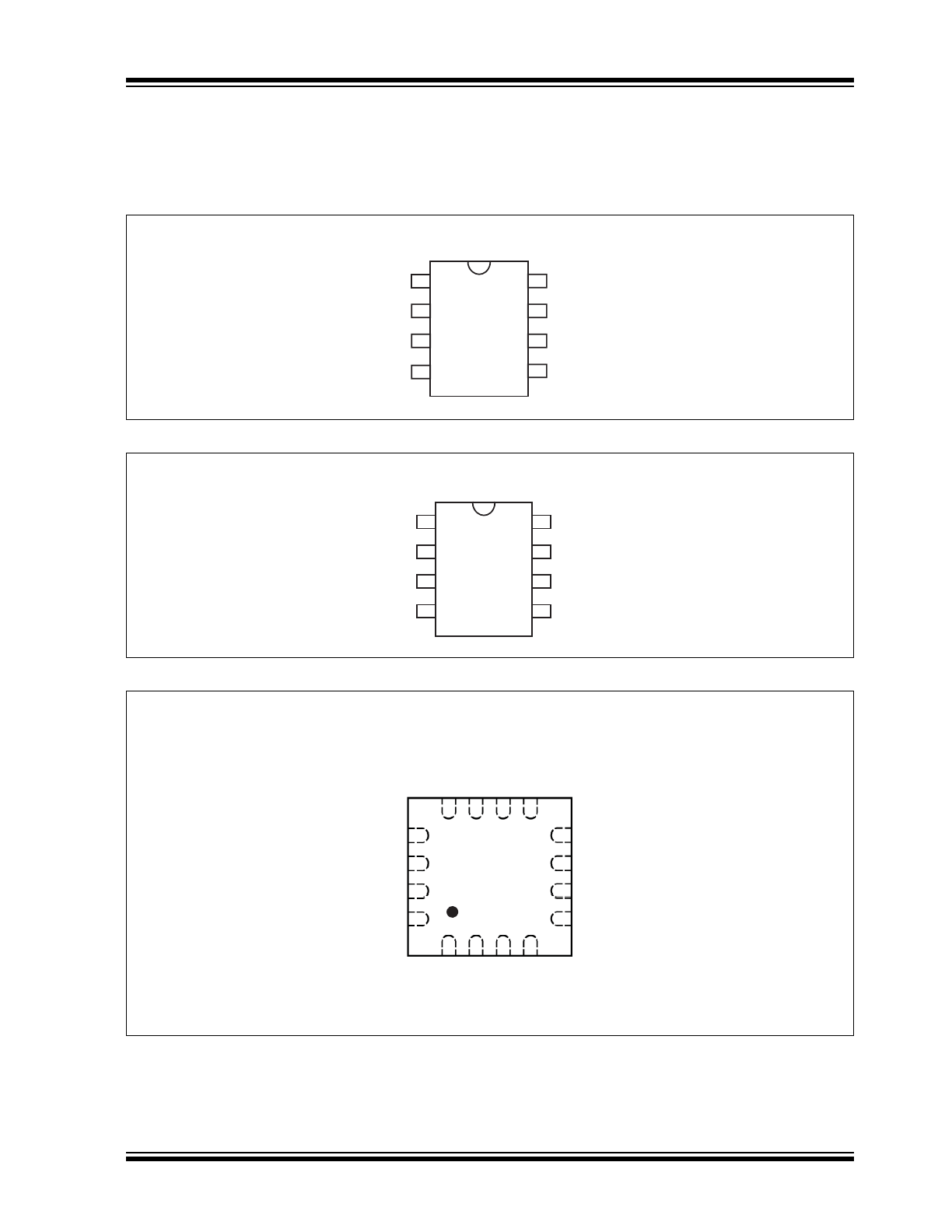
Pin Configurations
PL130-07
(Top View)
PL
130-07
1
2
3
4
5
6
7
8
GND
CLK_IN
GND
VDD
DRV_SEL^
GND
CLK_OUT
VDD
SOIC-8L
PL130-07(A)
(Top View)
PL13
0-
07
(A)
1
2
3
4
5
6
7
8
VDD
DRV_SEL
GND
OE
CLK_OUT
DNC
CLK_IN
VDD
TSSOP-8L
PL130-07(A)
(Top View)
PL130-07(A)
CLK_OUT
N/C
GND
VDD
1
2
3
4
12
11
10
9
13
14
15
16
8
7
6
5
VDD
VD
D
GND
VD
D
GND
DRV_SEL
GND
OE
GN
D
GN
D
CLK_IN
GN
D
QFN-16
PL130-07
DS20005598A-page 6
2016 Microchip Technology Inc.
TABLE 2-1:
PIN FUNCTION TABLE
Pin Name
SOIC-8L
TSSOP-8L
QFN-16L
Type
Description
GND
1, 3, 6
3
1, 2, 4, 5,
9, 14, 15
P
Ground.
V
DD
4, 7
1, 7
7, 10,
11, 12
P
Power supply.
DRV_SEL
8
2
13
I
Drive Select input: ‘1’ for standard drive,
‘0’ for high drive output. Internal pull-up
(default is ‘1’).
CLK_IN
2
5
3
I
Clock input signal. The frequency of this
signal will be reproduced at the output
(after translation to CMOS level).
CLK_OUT
5
8
8
O
CMOS clock output.
OE
N/A
4
16
I
Output Enable. See
Table 2-2
.
TABLE 2-2:
OE LOGIC TABLE
Part Number
OE State
Output Buffer State
PL130-07
0
Tri-State
1 (default)
Active
PL130-07A
0 (default)
Active
1
Tri-State
2016 Microchip Technology Inc.
DS20005598A-page 7
PL130-07
3.0
PACKAGING INFORMATION
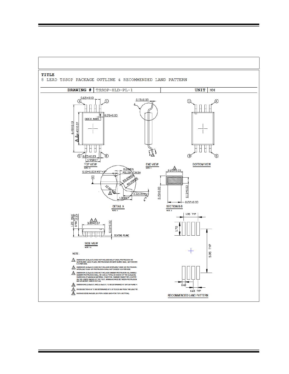
8 Lead TSSOP Package Outline and Recommended Land Pattern
Note:
For the most current package drawings, please see the Microchip Packaging Specification located at
http://www.microchip.com/packaging
PL130-07
DS20005598A-page 8
2016 Microchip Technology Inc.
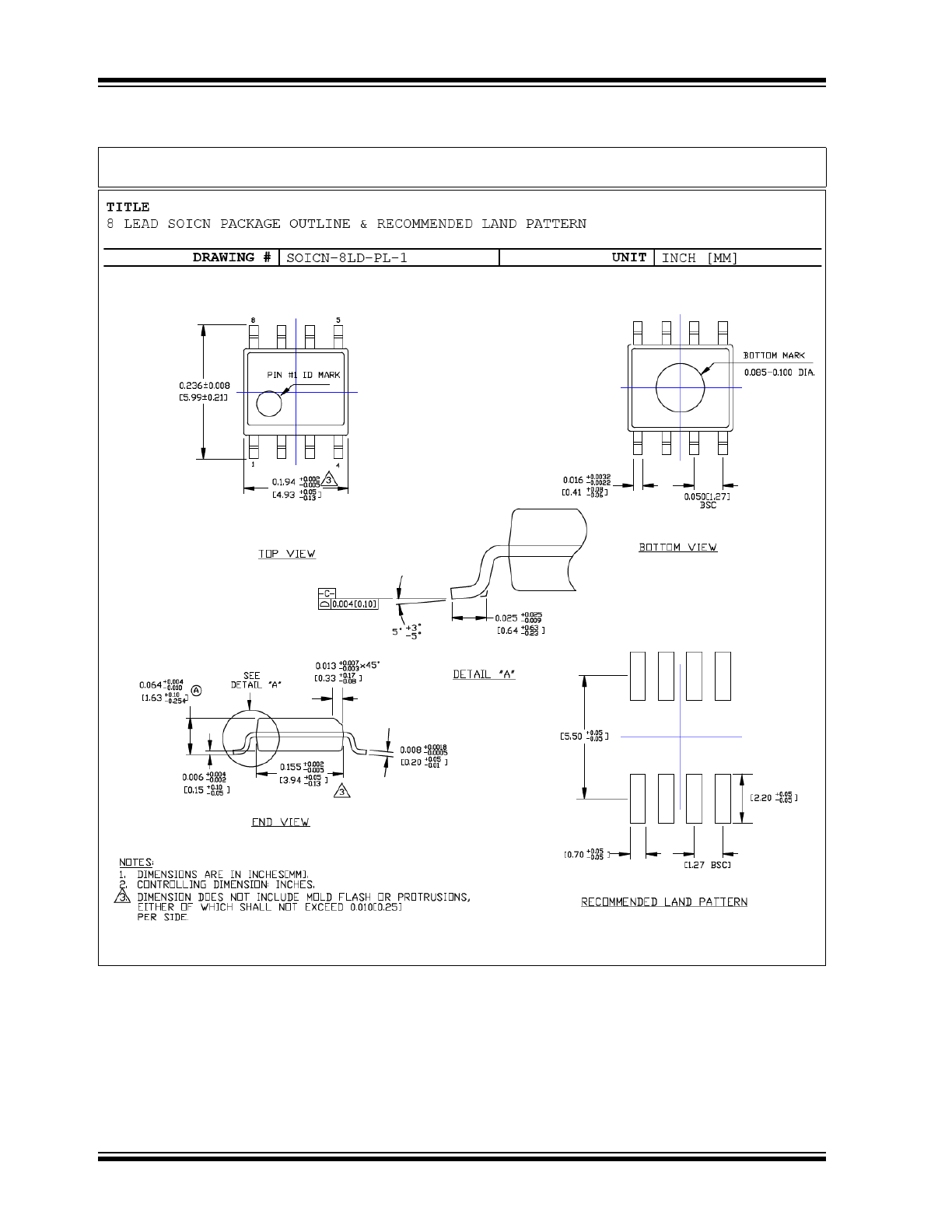
8-Lead SOIC Package Outline and Recommended Land Pattern
Note:
For the most current package drawings, please see the Microchip Packaging Specification located at
http://www.microchip.com/packaging
2016 Microchip Technology Inc.
DS20005598A-page 9
PL130-07
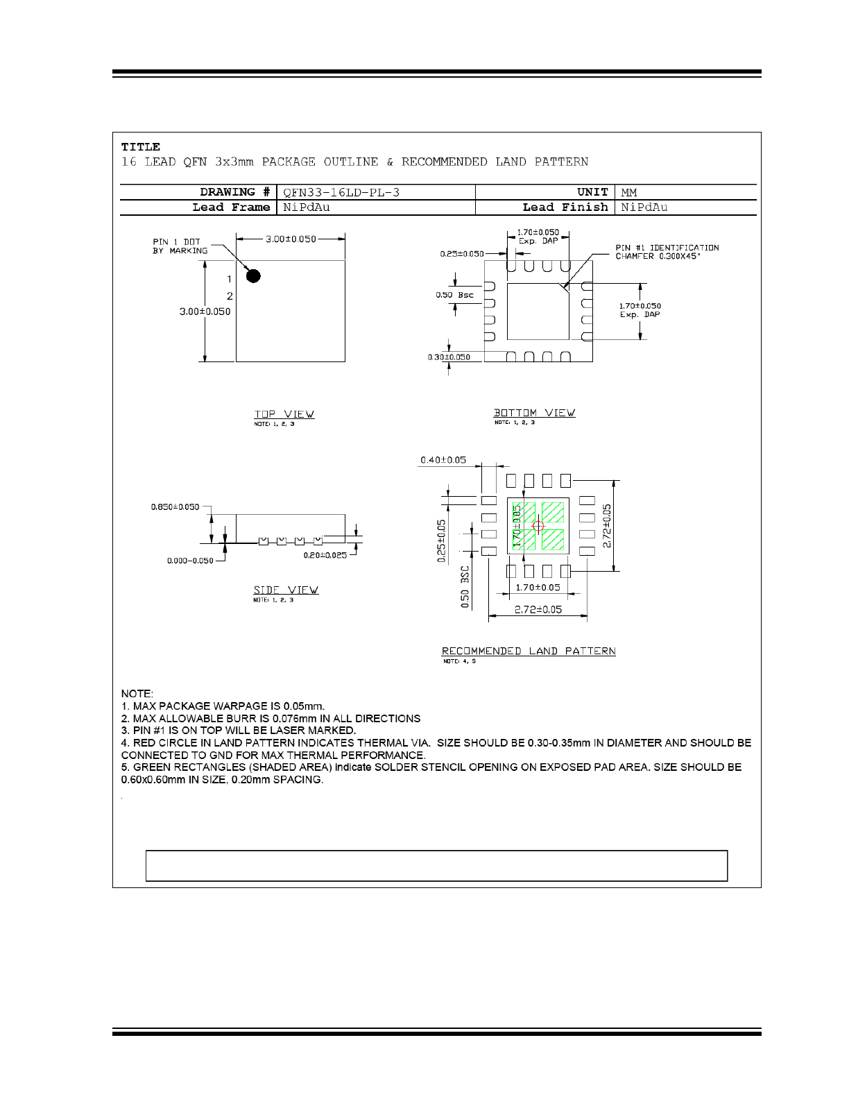
16-Lead QFN 3 mm x 3 mm Package Outline and Recommended Land Pattern
Note: For the most current package drawings, please see the Microchip Packaging Specification located at
http://www.microchip.com/packaging.

PL130-07
DS20005598A-page 10
2016 Microchip Technology Inc.
NOTES: