

© 2008 Microchip Technology Inc.
DS22063B-page 1
MCP1631/HV/MCP1631V/VHV
Features
• Programmable Switching Battery Charger
Designs
• High-Speed Analog PWM Controller
(2 MHz Operation)
• Combine with Microcontroller for “Intelligent”
Power System Development
• Peak Current Mode Control (MCP1631)
• Voltage Mode Control (MCP1631V)
• High Voltage Options Operate to +16V Input:
- MCP1631HV Current Mode
- MCP1631VHV Voltage Mode
• Regulated Output Voltage Options:
- +5.0V or +3.3V
- 250 mA maximum current
• External Oscillator Input sets Switching
Frequency and Maximum Duty Cycle Limit
• External Reference Input Sets Regulation Voltage
or Current
• Error Amplifier, Battery Current I
SNS
Amplifier,
Battery Voltage V
SNS
Amplifier Integrated
• Integrated Overvoltage Comparator
• Integrated High Current Low Side MOSFET
Driver (1A Peak)
• Shutdown mode reduces IQ to 2.4 µA (typical)
• Internal Overtemperature Protection
• Undervoltage Lockout (UVLO)
• Package Options:
- 4 mm x 4 mm 20-Lead QFN
(MCP1631/MCP1631V only)
- 20-Lead TSSOP (All Devices)
- 20-Lead SSOP (All Devices)
Applications
• High Input Voltage Programmable Switching
Battery Chargers
• Supports Multiple Chemistries Li-Ion, NiMH, NiCd
Intelligent and Pb-Acid
• LED Lighting Applications
• Constant Current SEPIC Power Train Design
• USB Input Programmable Switching Battery
Chargers
General Description
The MCP1631/MCP1631V is a high-speed
analog pulse width modulator (PWM) used to develop
intelligent power systems. When combined with a
microcontroller, the MCP1631/MCP1631V will control
the power system duty cycle providing output voltage
or current regulation. The microcontroller can be used
to adjust output voltage or current, switching frequency
and maximum duty cycle while providing additional
features making the power system more intelligent,
robust and adaptable.
Typical applications for the MCP1631/MCP1631V
include programmable switch mode battery chargers
capable of charging multiple chemistries, like Li-Ion,
NiMH, NiCd and Pb-Acid configured as single or
m u l t i p l e c e l l s . B y c o m b i n i n g w i t h a s m a l l
microcontroller, intelligent LED lighting designs and
programmable SEPIC topology voltage and current
sources can also be developed.
The MCP1631/MCP1631V inputs were developed to
be attached to the I/O pins of a microcontroller for
design flexibility. Additional features integrated into the
MCP1631HV/MCP1631VHV provide signal condition-
ing and protection features for battery charger or
constant current source applications.
For applications that operate from a high voltage input,
the MCP1631HV and MCP1631VHV device options
can be used to operate directly from a +3.5V to +16V
input. For these applications, an additional low drop out
+5V or +3.3V regulated output is available and can
provide current up to 250 mA to power a microcontroller
and auxiliary circuits.
High-Speed, Pulse Width Modulator
MCP1631/HV/MCP1631V/VHV
DS22063B-page 2
© 2008 Microchip Technology Inc.
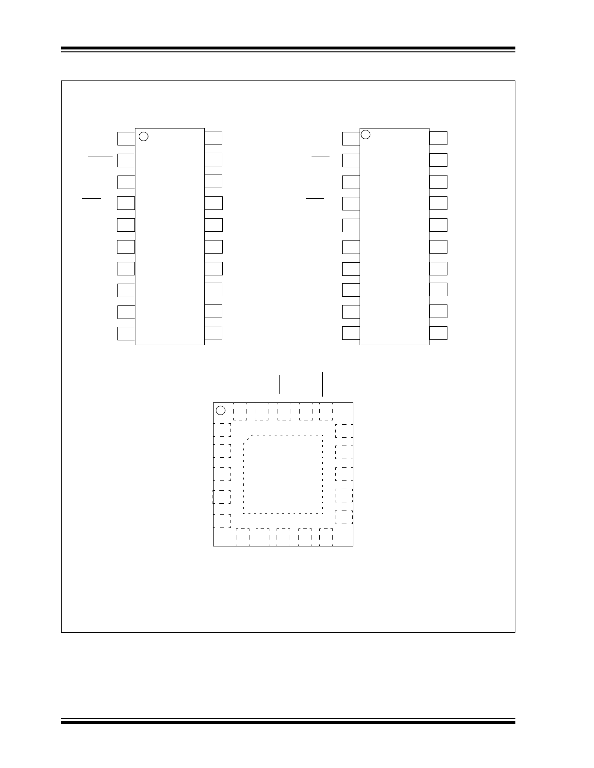
Package Types
1
2
3
COMP
PGND
4
5
6
7
8
9
10
20
19
18
17
16
15
14
13
12
11
20-Lead SSOP and TSSOP
MCP1631/MCP1631V
SHDN
OSC
IN
OSC
DIS
OV
IN
V
REF
A
GND
NC
NC
NC
A
VDD_IN
VS
IN
IS
IN
VS
OUT
IS
OUT
FB
CS/V
RAMP
P
VDD
V
EXT
1
2
3
COMP
PGND
4
5
6
7
8
9
10
20
19
18
17
16
15
14
13
12
11
20-Lead SSOP and TSSOP
MCP1631HV/MCP1631VHV
SHDN
OSC
IN
OSC
DIS
OV
IN
V
REF
A
GND
NC
NC
A
VDD_OUT
VS
IN
IS
IN
VS
OUT
IS
OUT
FB
CS/V
RAMP
P
VDD
V
EXT
V
IN
COMP
P
GND
SHDN
A
GND
NC
NC
VS
IN
IS
IN
VS
OU
T
IS
OU
T
FB
CS/V
RAMP
P
VDD
V
EXT
A
VDD_IN
1
2
3
4
5
6
7
8
9
10
15
14
13
12
11
20
19
1 8
17
16
NC
OSC
IN
OSC
DI
S
OV
IN
V
REF
EP
20 Lead 4x4 QFN
MCP1631/MCP1631V
21
© 2008 Microchip Technology Inc.
DS22063B-page 3
MCP1631/HV/MCP1631V/VHV
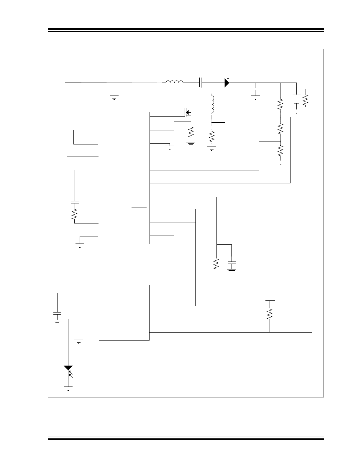
Typical Application Diagram
COMP
P
GND
SHDN
OSC
IN
OSC
DIS
OV
IN
V
REF
A
GND
NC
NC
A
VDD_OUT
VS
IN
IS
IN
VS
OUT
IS
OUT
FB
CS
P
VDD
V
EXT
L1A
C
IN
SCHOTTKY
DIODE
C
OUT
L1B
C
C
MCP1631HV
V
IN
R
THERM
A
VDD_OUT
GP0/C
C
GP5
GP3
GP1/C
PIC12F683
LED
R
GND
GP4
CCP1
V
DD
V
IN
Range +5.5V to +16V
Multi-cell, Multi-Chemistry Charger
MCP1631/HV/MCP1631V/VHV
DS22063B-page 4
© 2008 Microchip Technology Inc.
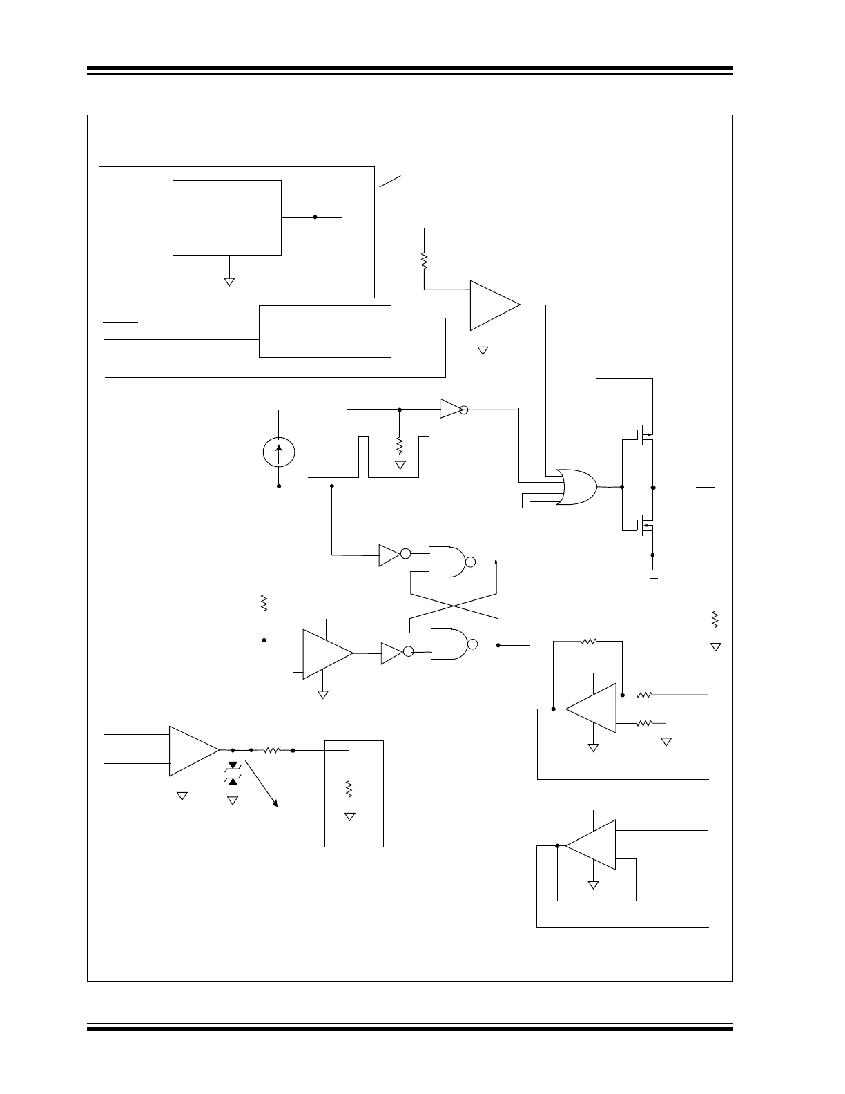
Functional Block Diagram
(1)
MCP1631HV/VHV High Speed PIC PWM
R
S
Q
Q
A1
+
-
V
REF
FB
C1
+
-
CS/VR
AMP
OSC
IN
P
VDD
COMP
P
GND
V
EXT
2R
2.7V Clamp
OT
UVLO
100 kΩ
0.1 µA
V
DD
R
+
-
R
R
10R
+
-
A2
A3
+3.3V or +5.0V
LDO
250 mA
V
IN
A
VDD_OUT
/ A
VDD_IN
V
DD
Shutdown Control
A3 Remains On
SHDN
IS
IN
IS
OUT
VS
IN
VS
OUT
C2
+
-
V
DD
A
GND
OV
IN
Overvoltage Comp
w/ Hysteresis
Internal
1.2V V
REF
OSC
DIS
100 kΩ
Remove for MCP1631V
and MCP1631VHV Options
Internal Regulator for MCP1631HV and MCP1631VHV
Options Only; For MCP1631 and MCP1631V AV
DD_IN
is input
V
DD
V
DD
V
DD
V
DD
V
DD
Note 1: For Shutdown control, amplifier A3 remains functional so
battery voltage can be sensed during discharge phase.
2: For HV options, internal Low Drop Out Regulator provides
+3.3V or +5.0V bias to V
DD
.
© 2008 Microchip Technology Inc.
DS22063B-page 5
MCP1631/HV/MCP1631V/VHV
1.0
ELECTRICAL
CHARACTERISTICS
Absolute Maximum Ratings †
V
IN
- GND (MCP1631/V)................................................+6.5V
V
IN
- GND (MCP1631HV/VHV)....................................+18.0V
All Other I/O ..............................(GND - 0.3V) to (V
DD
+ 0.3V)
LX to GND............................................. -0.3V to (V
DD
+ 0.3V)
V
EXT
Output Short Circuit Current ........................ Continuous
Storage temperature .....................................-65°C to +150°C
Maximum Junction Temperature...................-40°C to +150°C
Operating Junction Temperature...................-40°C to +125°C
ESD Protection On All Pins:
HBM ................................................................................. 4 kV
MM ..................................................................................400V
† Notice: Stresses above those listed under "Maximum
Ratings" may cause permanent damage to the device. This is
a stress rating only and functional operation of the device at
those or any other conditions above those indicated in the
operational sections of this specification is not intended.
Exposure to maximum rating conditions for extended periods
may affect device reliability.
DC CHARACTERISTICS
Electrical Specifications: Unless otherwise noted, V
IN
= 3.0V to 5.5V, F
OSC
= 1 MHz with 10% Duty Cycle, C
IN
= 0.1 µF,
V
DD
for typical values = 5.0V, T
A
for typical values
= +25°C, T
A
= -40°C to +125°C for all minimum and maximums.
Parameters
Sym
Min
Typ
Max
Units
Conditions
Input Characteristics
Input Voltage (MCP1631/V)
V
DD
3.0
—
5.5
V
Non-HV Options
Input Voltage
(MCP1631HV/VHV)
V
DD
3.5
—
16.0
V
HV Options (Note 2)
Undervoltage Lockout
(MCP1631/V)
UVLO
2.7
2.8
3.0
V
V
IN
Falling, V
EXT
low when input
below UVLO threshold
Undervoltage Lockout Hysteresis
(MCP1631/MCP1631V)
UVLO
_HYS
40
64
100
mV
UVLO Hysteresis
Input Quiescent Current
(MCP1631/V, MCP1631HV,VHV)
I(V
IN
)
—
3.7
5
mA
SHDN = V
DD
=OSC
DIS
Shutdown Current
I_AVDD for MCP1631/V
I_VIN for MCP1631HV/VHV
I
IN_SHDN
—
2.4
4.4
12
17
µA
µA
SHDN = GND =OSC
DIS
,
Note: Amplifier A3 remains
powered during Shutdown.
OSC
IN
, OSC
DIS
and SHDN Input Levels
Low Level Input Voltage
V
IL
—
—
0.8
V
High Level Input Voltage
V
IH
2.0
—
—
V
Input Leakage Current
I
LEAK
0.005
1
µA
External Oscillator Range
F
OSC
—
—
2
MHz
Maximum operating frequency is
dependent upon circuit topology
and duty cycle.
Minimum Oscillator High Time
Minimum Oscillator Low Time
T
OH
_MIN.
T
OL
_MIN.
—
10
—
ns
Oscillator Rise and Fall Time
T
R
and T
F
0.01
—
10
µs
Note 1
Oscillator Input Capacitance
C
OSC
—
5
—
pf
Note 1:
External Oscillator Input (OSC
IN
) rise and fall times between 10 ns and 10 µs were determined during device
characterization testing. Signal levels between 0.8V and 2.0V with rise and fall times measured between 10% and 90%
of maximum and minimum values. Not production tested. Additional timing specifications were fully characterized and
specified that are not production tested.
2:
The minimum V
IN
must meet two conditions: V
IN
≥ 3.5V and V
IN
≥ (V
OUT(MAX)
+ V
DROPOUT(MAX)
).
3:
TCV
OUT
= (V
OUT-HIGH
- V
OUT-LOW
) *10
6
/ (V
R
*
ΔTemperature), V
OUT-HIGH
= highest voltage measured over the
temperature range. V
OUT-LOW
= lowest voltage measured over the temperature range.
4:
Load regulation is measured at a constant junction temperature using low duty cycle pulse testing. Changes in output
voltage due to heating effects are determined using thermal regulation specification TCV
OUT
.
5:
Dropout voltage is defined as the input to output differential at which the output voltage drops 2% below its measured
value with an applied input voltage of V
OUT(MAX)
+ V
DROPOUT(MAX)
or 3.5V, whichever is greater.
MCP1631/HV/MCP1631V/VHV
DS22063B-page 6
© 2008 Microchip Technology Inc.
External Reference Input
Reference Voltage Input
V
REF
0
—
AV
DD
V
The reference input is capable of
rail-to-rail operation.
Internal Driver)
R
DSON
P-channel
R
DSon_P
—
7.2
15
Ω
R
DSON
N-channel
R
DSon_N
—
3.8
15
Ω
V
EXT
Rise Time
T
RISE
—
2.5
18
ns
C
L
= 100 pF
Typical for V
IN
= 5V (Note 1)
V
EXT
Fall Time
T
FALL
—
2.7
18
ns
C
L
= 100 pF
Typical for V
IN
= 5V (Note 1)
Error Amplifier (A1)
Input Offset Voltage
V
OS
-5
-0.6
+5
mV
A1 Input Bias Current
I
BIAS
—
0.05
1
µA
Error Amplifier PSRR
PSRR
—
85.4
—
dB
V
IN
= 3.0V to 5.0V, V
CM
= 1.2V
Common Mode Input Range
V
CM
GND - 0.3
—
V
IN
V
Common Mode Rejection Ratio
—
90
—
dB
V
IN
= 5V, V
CM
= 0V to 2.5V
Open-loop Voltage Gain
A
VOL
80
95
—
dB
R
L
= 5 kΩ to V
IN
/2,
100 mV < V
EAOUT
< V
IN
- 100 mV,
V
CM
= 1.2V
Low-level Output
V
OL
—
25
GND + 65
mV
RL = 5 kΩ to V
IN
/2
Gain Bandwidth Product
GBWP
—
3.5
—
MHz
V
IN
= 5V
Error Amplifier Sink Current
I
SINK
4
12
—
mA
V
IN
= 5V, V
REF
= 1.2V,
V
FB
= 1.4V, V
COMP
= 2.0V
Error Amplifier Source Current
I
SOURCE
-2
-9.8
—
mA
V
IN
= 5V, V
REF
= 1.2V,
V
FB
= 1.0V, V
COMP
= 2.0V,
Absolute Value
Current Sense (CS) Amplifier (A2)
Input Offset Voltage
V
OS
-3.0
1.2
+3.0
mV
CS Input Bias Current
I
BIAS
—
0.13
1
µA
CS Amplifier PSRR
PSRR
—
65
—
dB
V
IN
= 3.0V to 5.0V, V
CM
= 0.12V,
GAIN = 10
Closed-loop Voltage Gain
A2
VCL
—
10
—
V/V
R
L
= 5 kΩ to V
IN
/2,
100 mV < V
OUT
< V
IN
- 100 mV,
V
CM
= +0.12V
Low-level Output
V
OL
5
11
GND + 50
mV
RL = 5 kΩ to V
IN
/2
CS Sink Current
I
SINK
5
17.7
—
mA
CS Amplifier Source Current
I
SOURCE
-5
-19.5
—
mA
Voltage Sense (VS) Amplifier (A3)
Input Offset Voltage
V
OS
-5
0.9
+5
mV
VS Input Bias Current
I
BIAS
—
0.001
1
µA
DC CHARACTERISTICS (CONTINUED)
Electrical Specifications: Unless otherwise noted, V
IN
= 3.0V to 5.5V, F
OSC
= 1 MHz with 10% Duty Cycle, C
IN
= 0.1 µF,
V
DD
for typical values = 5.0V, T
A
for typical values
= +25°C, T
A
= -40°C to +125°C for all minimum and maximums.
Parameters
Sym
Min
Typ
Max
Units
Conditions
Note 1:
External Oscillator Input (OSC
IN
) rise and fall times between 10 ns and 10 µs were determined during device
characterization testing. Signal levels between 0.8V and 2.0V with rise and fall times measured between 10% and 90%
of maximum and minimum values. Not production tested. Additional timing specifications were fully characterized and
specified that are not production tested.
2:
The minimum V
IN
must meet two conditions: V
IN
≥ 3.5V and V
IN
≥ (V
OUT(MAX)
+ V
DROPOUT(MAX)
).
3:
TCV
OUT
= (V
OUT-HIGH
- V
OUT-LOW
) *10
6
/ (V
R
*
ΔTemperature), V
OUT-HIGH
= highest voltage measured over the
temperature range. V
OUT-LOW
= lowest voltage measured over the temperature range.
4:
Load regulation is measured at a constant junction temperature using low duty cycle pulse testing. Changes in output
voltage due to heating effects are determined using thermal regulation specification TCV
OUT
.
5:
Dropout voltage is defined as the input to output differential at which the output voltage drops 2% below its measured
value with an applied input voltage of V
OUT(MAX)
+ V
DROPOUT(MAX)
or 3.5V, whichever is greater.
© 2008 Microchip Technology Inc.
DS22063B-page 7
MCP1631/HV/MCP1631V/VHV
VS Amplifier PSRR
PSRR
—
65
—
dB
V
IN
= 3.0V to 5.0V, V
CM
= 1.2V
Common Mode Input Range
V
CM
GND
—
AV
DD
V
Rail to Rail Input
Closed-loop Voltage Gain
A3
VCL
—
1
—
V/V
R
L
= 5 kΩ to V
IN
/2,
100 mV < V
EAOUT
< V
IN
- 100 mV,
V
CM
= 1.2V
Low-level Output
V
OL
—
38
GND + 85
mV
RL = 5 kΩ to V
IN
/2
VS Amplifier Sink Current
I
SINK
1
5
—
mA
VS Amplifier Source Current
I
SOURCE
-2
-5
—
mA
Peak Current Sense Input (C1)
Maximum Current Sense Signal
MCP1631/MCP1631HV
V
CS_MAX
0.85
0.9
0.98
V
Maximum Ramp Signal
MCP1631V/MCP1631VHV
V
RAMP
2.7
2.78
2.9
V
V
IN
> 4V
Maximum CS input range limited
by comparator input common
mode range. V
CS_MAX
= V
IN
-1.4V
Current Sense Input Bias Current
I
CS_B
—
-0.1
—
µA
V
IN
= 5V
Delay From CS to V
EXT
MCP1631
T
CS_VEXT
—
8.5
25
ns
Note 1
Minimum Duty Cycle
DC
MIN
—
—
0
%
V
FB
= V
REF
+ 0.1V,
V
CS
= GND
Overvoltage Sense Comparator (C2)
OV Reference Voltage High
OV
_VREF_H
—
1.23
—
V
OV Reference Voltage Low
OV
_VREF_L
1.15
1.18
1.23
V
OV Hysteresis
OV_HYS
—
50
—
mV
Overvoltage Comparator
Hysteresis
OV_IN Bias Current
OV_
IBIAS
—
0.001
1
µA
Delay From OV to V
EXT
T
OV_VEXT
—
63
150
ns
Delay from OV detection to PWM
termination (Note 1)
OV Input Capacitance
C_
OV
—
5
—
pF
Internal Regulator HV Options Input / Output Characteristics
Input Operating Voltage
V
IN
3.5
—
16.0
V
Note 2
Maximum Output Current
I
OUT_mA
250
—
—
mA
Output Short Circuit Current
I
OUT_SC
—
400
—
mA
V
IN
= V
IN(MIN)
(Note 2),
V
OUT
= GND,
Current (average current)
measured 10 ms after short is
applied.
Output Voltage Regulation
V
OUT
V
R
-3.0%
V
R
±0.4%
V
R
+3.0%
V
V
R
= 3.3V or 5.0V
V
OUT
Temperature Coefficient
TCV
OUT
—
50
150
ppm/
°C
Note 3
DC CHARACTERISTICS (CONTINUED)
Electrical Specifications: Unless otherwise noted, V
IN
= 3.0V to 5.5V, F
OSC
= 1 MHz with 10% Duty Cycle, C
IN
= 0.1 µF,
V
DD
for typical values = 5.0V, T
A
for typical values
= +25°C, T
A
= -40°C to +125°C for all minimum and maximums.
Parameters
Sym
Min
Typ
Max
Units
Conditions
Note 1:
External Oscillator Input (OSC
IN
) rise and fall times between 10 ns and 10 µs were determined during device
characterization testing. Signal levels between 0.8V and 2.0V with rise and fall times measured between 10% and 90%
of maximum and minimum values. Not production tested. Additional timing specifications were fully characterized and
specified that are not production tested.
2:
The minimum V
IN
must meet two conditions: V
IN
≥ 3.5V and V
IN
≥ (V
OUT(MAX)
+ V
DROPOUT(MAX)
).
3:
TCV
OUT
= (V
OUT-HIGH
- V
OUT-LOW
) *10
6
/ (V
R
*
ΔTemperature), V
OUT-HIGH
= highest voltage measured over the
temperature range. V
OUT-LOW
= lowest voltage measured over the temperature range.
4:
Load regulation is measured at a constant junction temperature using low duty cycle pulse testing. Changes in output
voltage due to heating effects are determined using thermal regulation specification TCV
OUT
.
5:
Dropout voltage is defined as the input to output differential at which the output voltage drops 2% below its measured
value with an applied input voltage of V
OUT(MAX)
+ V
DROPOUT(MAX)
or 3.5V, whichever is greater.
MCP1631/HV/MCP1631V/VHV
DS22063B-page 8
© 2008 Microchip Technology Inc.
TEMPERATURE SPECIFICATIONS
Line Regulation
ΔV
OUT
/
(V
OUT
X
Δ
V
IN
)
-0.3
±0.1
+0.3
%/V
(V
OUT(MAX)
+ V
DROPOUT(MAX)
)
≤
V
IN
≤ 16V Note 2
Load Regulation
ΔV
OUT
/
V
OUT
-2.5
±1.0
+2.5
%
I
L
= 1.0 mA to 250 mA, Note 4
Dropout Voltage
Note 2, Note 5
V
DROPOUT
—
330
650
mV
I
L
= 250 mA, V
R
= 5.0V
—
525
725
mV
I
L
= 250 mA, V
R
= 3.3V
Output Delay Time
T
DELAY
—
1000
—
µs
V
IN
= 0V to 6V, V
OUT
= 90% V
R
,
R
L
= 50Ω resistive
Output Noise
e
N
—
8
—
µV/
(Hz)
1/2
I
L
= 50 mA, f = 1 kHz, C
OUT
=
1 µF
Power Supply Ripple Rejection
Ratio
PSRR
—
44
—
dB
f = 100 Hz, C
OUT
= 1 µF,
I
L
= 100 µA,
V
INAC
=100 mV pk-pk,
C
IN
= 0 µF, V
R
= 1.2V
Protection Features
Thermal Shutdown
T
SHD
—
150
—
°C
Thermal Shutdown Hysteresis
T
SHD_HYS
—
18
—
°C
Electrical Specifications: Unless otherwise indicated, all limits are specified for: V
IN
+ 3.0V to 5.5V
Parameters
Sym
Min
Typ
Max
Units
Conditions
Temperature Ranges
Operating Junction Temperature
Range
T
J
-40
—
+125
°C
Steady State
Storage Temperature Range
T
A
-65
—
+150
°C
Maximum Junction Temperature
T
J
—
—
+150
°C
Transient
Package Thermal Resistances
Thermal Resistance, 20L-TSSOP
θ
JA
—
90
—
°C/W
Typical 4 Layer board with
interconnecting vias
Thermal Resistance, 20L-SSOP
θ
JA
—
89.3
—
°C/W
Typical 4 Layer board with
interconnecting vias
Thermal Resistance, 20L-QFN
θ
JA
—
43
—
°C/W
Typical 4 Layer board with
interconnecting vias
DC CHARACTERISTICS (CONTINUED)
Electrical Specifications: Unless otherwise noted, V
IN
= 3.0V to 5.5V, F
OSC
= 1 MHz with 10% Duty Cycle, C
IN
= 0.1 µF,
V
DD
for typical values = 5.0V, T
A
for typical values
= +25°C, T
A
= -40°C to +125°C for all minimum and maximums.
Parameters
Sym
Min
Typ
Max
Units
Conditions
Note 1:
External Oscillator Input (OSC
IN
) rise and fall times between 10 ns and 10 µs were determined during device
characterization testing. Signal levels between 0.8V and 2.0V with rise and fall times measured between 10% and 90%
of maximum and minimum values. Not production tested. Additional timing specifications were fully characterized and
specified that are not production tested.
2:
The minimum V
IN
must meet two conditions: V
IN
≥ 3.5V and V
IN
≥ (V
OUT(MAX)
+ V
DROPOUT(MAX)
).
3:
TCV
OUT
= (V
OUT-HIGH
- V
OUT-LOW
) *10
6
/ (V
R
*
ΔTemperature), V
OUT-HIGH
= highest voltage measured over the
temperature range. V
OUT-LOW
= lowest voltage measured over the temperature range.
4:
Load regulation is measured at a constant junction temperature using low duty cycle pulse testing. Changes in output
voltage due to heating effects are determined using thermal regulation specification TCV
OUT
.
5:
Dropout voltage is defined as the input to output differential at which the output voltage drops 2% below its measured
value with an applied input voltage of V
OUT(MAX)
+ V
DROPOUT(MAX)
or 3.5V, whichever is greater.
© 2008 Microchip Technology Inc.
DS22063B-page 9
MCP1631/HV/MCP1631V/VHV
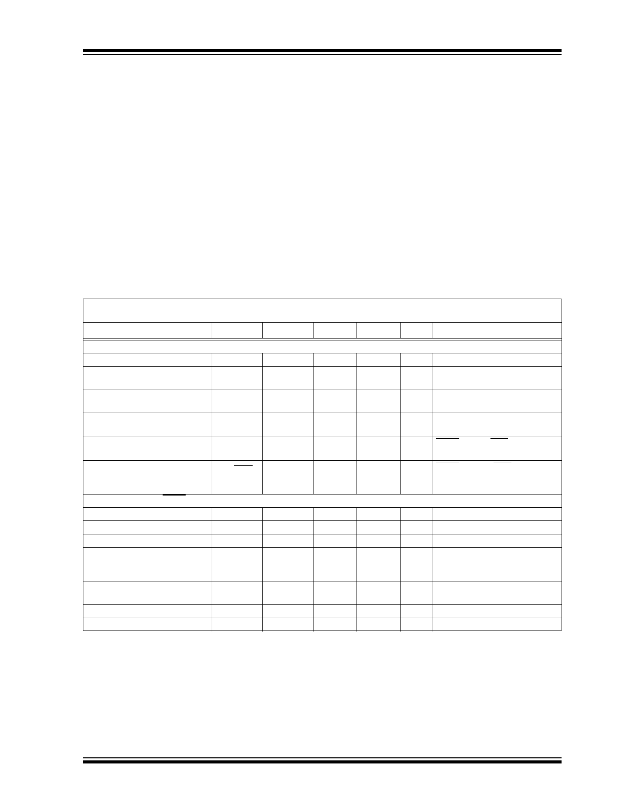
2.0
TYPICAL PERFORMANCE CURVES
Note:
Unless otherwise noted, V
IN
= 3.0V to 5.5V, F
OSC
= 1 MHz with 10% Duty Cycle, C
IN
= 0.1 µF, V
IN
for typical values = 5.0V, T
A
for typical values
= +25°C.
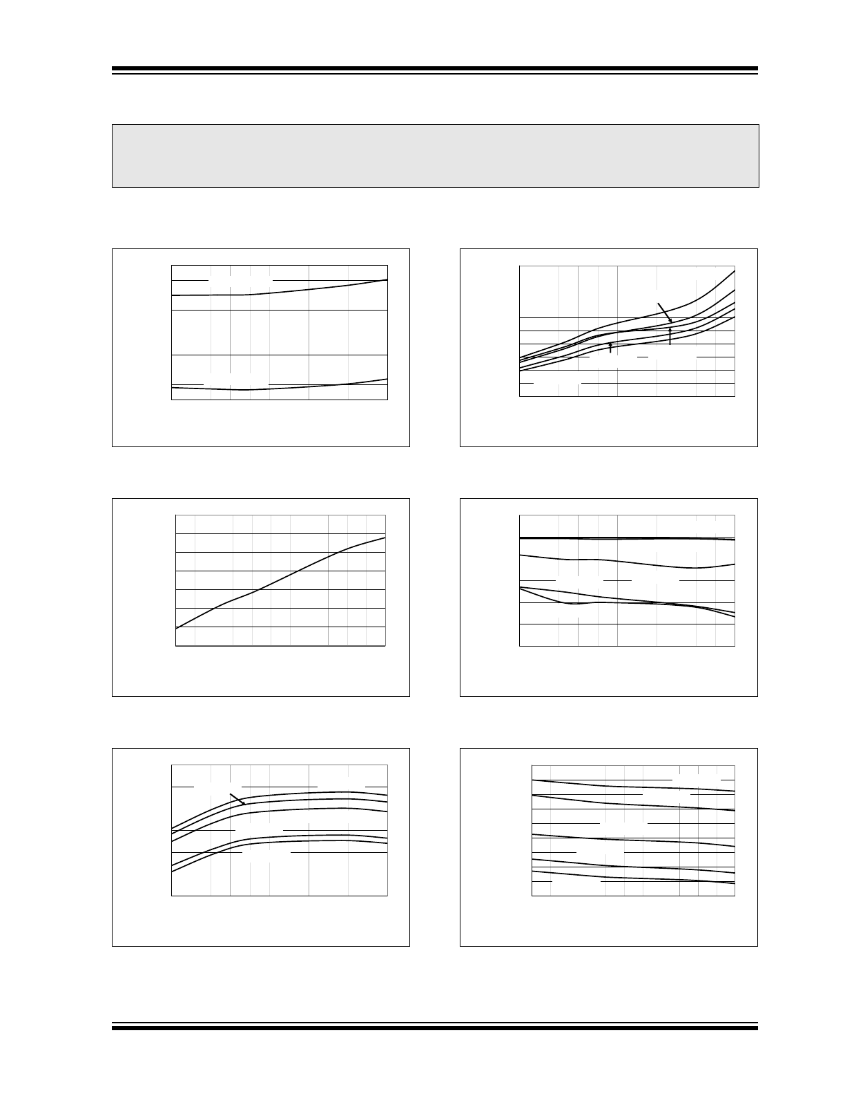
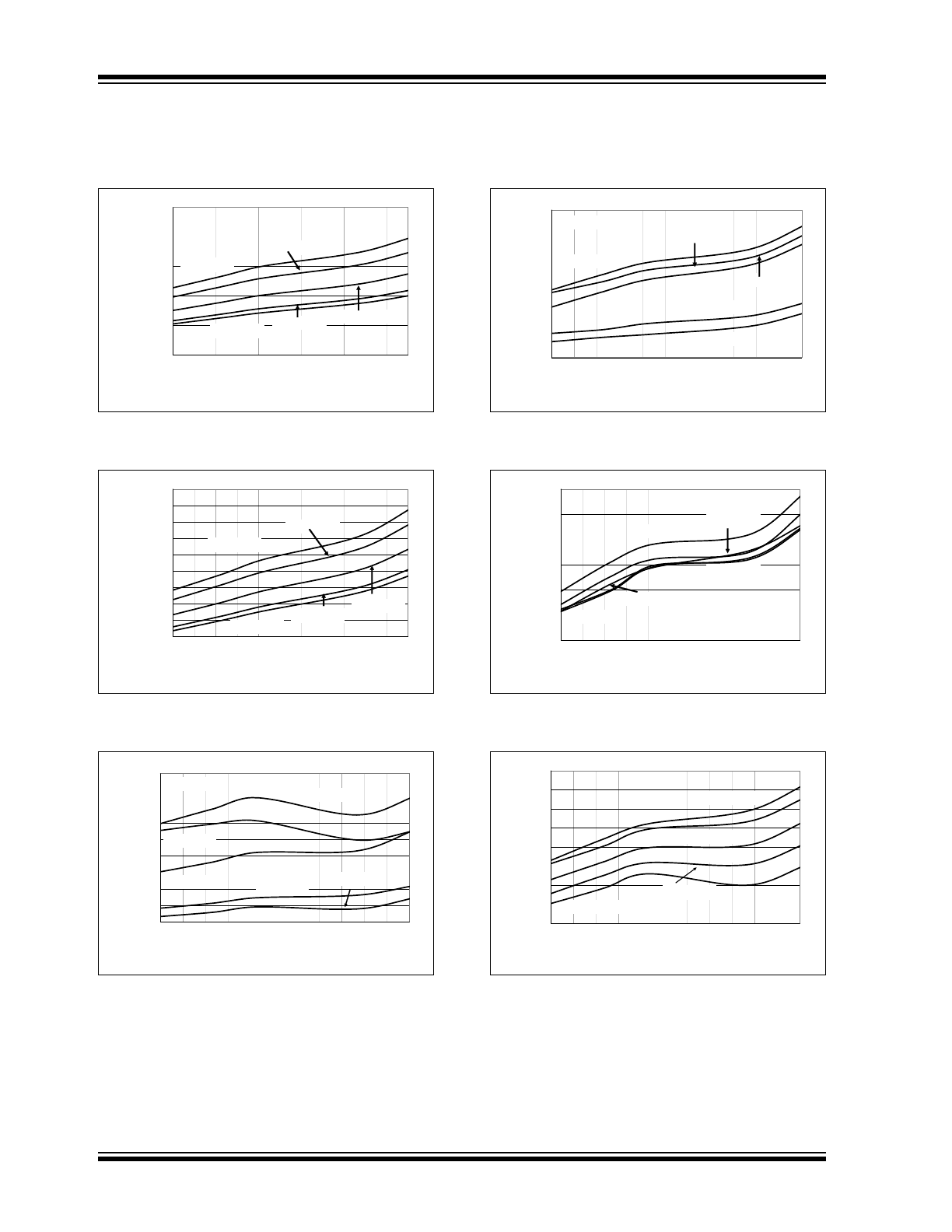
FIGURE 2-1:
Undervoltage Lockout vs.
Temperature.
FIGURE 2-2:
Undervoltage Lockout
Hysteresis vs. Temperature.
FIGURE 2-3:
Input Quiescent Current vs.
Temperature.
FIGURE 2-4:
Shutdown Current vs.
Temperature (MCP1631/MCP1631V).
FIGURE 2-5:
Oscillator Input Threshold
vs. Temperature.
FIGURE 2-6:
Oscillator Disable Input
Threshold vs. Temperature.
Note:
The graphs and tables provided following this note are a statistical summary based on a limited number of
samples and are provided for informational purposes only. The performance characteristics listed herein are
not tested or guaranteed. In some graphs or tables, the data presented may be outside the specified
operating range (e.g., outside specified power supply range) and therefore outside the warranted range.
2.8
2.81
2.82
2.83
2.84
2.85
2.86
2.87
2.88
2.89
-4
0
-2
5
-1
0
5
20
35
50
65
80
95
11
0
12
5
Ambient Temperature (°C)
Undervoltage Lockout
(V)
Device Turn On
Device Turn Off
0.061
0.062
0.063
0.064
0.065
0.066
0.067
0.068
-4
0
-2
5
-1
0
5
20
35
50
65
80
95
11
0
12
5
Ambient Temperature (°C)
UVLO Hyst
(V)
2.80
3.00
3.20
3.40
3.60
3.80
4.00
-4
0
-2
5
-1
0
5
20
35
50
65
80
95
11
0
12
5
Ambient Temperature (°C)
Input
Quiescent
Curr
ent (
m
A)
V
DD
= +3.0V
V
DD
= +3.3V
V
DD
= +4.0V
V
DD
= +5.0V
V
DD
= +5.5V
1.00
1.30
1.60
1.90
2.20
2.50
2.80
3.10
3.40
3.70
4.00
-4
0
-2
5
-1
0
5
20
35
50
65
80
95
11
0
12
5
Ambient Temperature (°C)
S
hut
down Current
(µA)
V
DD
= +3.0V
V
DD
= +3.3V
V
DD
= +4.0V
V
DD
= +5.0V
V
DD
= +5.5V
1.00
1.10
1.20
1.30
1.40
1.50
1.60
-4
0
-2
5
-1
0
5
20
35
50
65
80
95
11
0
12
5
Ambient Temperature (°C)
OSC_IN Input Threshold (V)
V
DD
= +3.0V
V
DD
= +3.3V
V
DD
= +4.0V
V
DD
= +5.0V
V
DD
= +5.5V
0.80
0.90
1.00
1.10
1.20
1.30
1.40
1.50
1.60
1.70
-4
0
-2
5
-1
0
5
20
35
50
65
80
95
11
0
12
5
Ambient Temperature (°C)
OSC_DIS
Input
Th
reshold
Vol
tage (
V
)
V
DD
= +3.0V
V
DD
= +3.3V
V
DD
= +4.0V
V
DD
= +5.0V
V
DD
= +5.5V
MCP1631/HV/MCP1631V/VHV
DS22063B-page 10
© 2008 Microchip Technology Inc.
Typical Performance Curves (Continued)
Note: Unless otherwise noted, V
IN
= 3.0V to 5.5V, F
OSC
= 1 MHz with 10% Duty Cycle, C
IN
= 0.1 µF,
V
IN
for typical values = 5.0V, T
A
for typical values = +25°C.
FIGURE 2-7:
V
EXT
P-Channel Driver
R
DSON
vs. Temperature.
FIGURE 2-8:
V
EXT
N-Channel Driver
R
DSON
vs. Temperature.
FIGURE 2-9:
V
EXT
Rise Time vs.
Temperature.
FIGURE 2-10:
V
EXT
Fall Time vs.
Temperature.
FIGURE 2-11:
Amplifier A1 Offset Voltage
vs. Temperature.
FIGURE 2-12:
Amplifier A1 Output Voltage
Low vs. Temperature.
4
6
8
10
12
14
-4
0
-2
5
-1
0
5
20
35
50
65
80
95
11
0
12
5
Ambient Temperature (°C)
E
X
T Output P-Chan
nel R
DS
ON
(ohms)
V
DD
= +3.0V
V
DD
= +3.3V
V
DD
= +4.0V
V
DD
= +5.0V
V
DD
= +5.5V
3.0
3.4
3.8
4.2
4.6
5.0
5.4
5.8
6.2
6.6
-4
0
-2
5
-1
0
5
20
35
50
65
80
95
11
0
12
5
Ambient Temperature (°C)
E
X
T Output N-
Channel
RD
SON (ohms)
V
DD
= +3.0V
V
DD
= +3.3V
V
DD
= +4.0V
V
DD
= +5.0V
V
DD
= +5.5V
2.0
2.3
2.6
2.9
3.2
3.5
3.8
4.1
4.4
4.7
-40
-25
-10
5
20
35
50
65
80
95
11
0
12
5
Ambient Temperature (°C)
V
EX
T
Rise
Time
(ns)
V
DD
= +3.0V
V
DD
= +3.3V
V
DD
= +4.0V
V
DD
= +5.0V
V
DD
= +5.5V
C
L
= 100 pF
2.0
2.3
2.6
2.9
3.2
3.5
3.8
4.1
4.4
4.7
5.0
-4
0
-2
5
-1
0
5
20
35
50
65
80
95
11
0
12
5
Ambient Temperature (°C)
V
EX
T
Fa
ll Time (ns)
V
DD
= +3.0V
V
DD
= +3.3V
V
DD
= +4.0V
V
DD
= +5.0V
V
DD
= +5.5V
C
L
= 100 pF
-0.80
-0.75
-0.70
-0.65
-0.60
-0.55
-0.50
-4
0
-2
5
-1
0
5
20
35
50
65
80
95
11
0
12
5
Ambient Temperature (°C)
A1
O
ff
set
Vol
tage
(m
V)
V
DD
= +3.0V
V
DD
= +3.3V
V
DD
= +4.0V
V
DD
= +5.0V
V
DD
= +5.5V
0
5
10
15
20
25
30
35
40
-4
0
-2
5
-1
0
5
20
35
50
65
80
95
11
0
12
5
Ambient Temperature (°C)
A1 V
OU
T
Low (
m
V
)
V
DD
= +3.0V
V
DD
= +3.3V
V
DD
= +4.0V
V
DD
= +5.0V
V
DD
= +5.5V