
2012-2016 Microchip Technology Inc.
DS20005293D-page 1
PAC1921
Features
• Configurable Measurement Type Output: Power,
Current or Bus Voltage
• Configurable Voltage Output (3V, 2V, 1.5V, 1V)
- All output values also available over SMBus
• New Device Topology
- Provides integrated average power
measurement
- Power measurements provided to
microcontroller with ADC inputs
- Unique lossless integrating architecture
allows operation at low sense voltages
- Output voltage proportional to selected
measurement
• High-Side Current Sensor
- 100 mV full-scale current sense voltage range
- Second-order delta-sigma ADC with 11-bit or
14-bit resolution
- Selectable current binary gain ranges: 1x
through 128x
• 1% Power Measurement Accuracy
• Auto-Zero Offset
• Auto Sleep State
- Automatically shifts to low-power state
(3.5 µA)
• Power Supply
- V
DD
= 3.3V nominal (operational range 3.0V
to 5.5V)
• Bus Range 0V to 32V
• No Input Filters Required
• Available in a 10-pin 3 mm x 3 mm VDFN RoHS
Compliant Package
Applications
• Diagnostic Equipment
• Servers
• Power Supplies
• Industrial and Power Management Systems
• Notebook and Desktop Computers
Description
The PAC1921 is a dedicated power-monitoring device
with a configurable analog output that can present
power, current or voltage. The PAC1921 is designed for
power measurement and diagnostic systems that
cannot allow for latency when performing high-speed
power management. Measurements are accumulated
in large lossless registers, allowing for integration
periods of 500 µs to 2.9 seconds. The measurement is
averaged and presented on the analog output with a
full scale range of 3V, 2V, 1.5V or 1.0V.
The PAC1921 has a READ/INT pin for host control of the
measurement integration period. This pin can be used to
synchronize readings of multiple buses between several
devices. Alternatively, PAC1921 is able to provide
outputs in a free-running mode. Information is provided
on the OUT pin and is available via SMBus if desired.
Data sampling and output attributes, such as the internal
ADC resolution (11-bit or 14-bit) and sample rate, are
configurable. The SMBus interface has more selections
for user-configurable options.
The PAC1921 is a 1% accurate power measurement
device that measures and cancels the zero offset from
the input pins. The PAC1921 was designed to monitor
power rails from 0-32V with a full-scale capability of
100 mV across the sense resistor. No input filters are
required for this device.
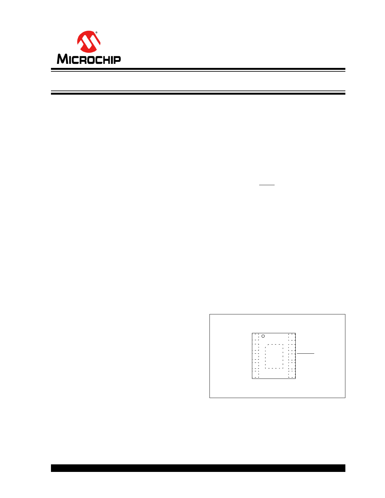
Package Types
SENSE -
SENSE +
OUT
SM_DATA
READ/INT
1
2
3
4
10
9
8
7 RESERVED
SM_CLK
V
DD
EP
11
6
5
ADDR_SEL
GND
PAC1921
3x3 VDFN*
*Includes Exposed Thermal Pad (EP), see
Table 3-1
High-Side Power/Current Monitor with Analog Output
PAC1921
DS20005293D-page 2
2012-2016 Microchip Technology Inc.
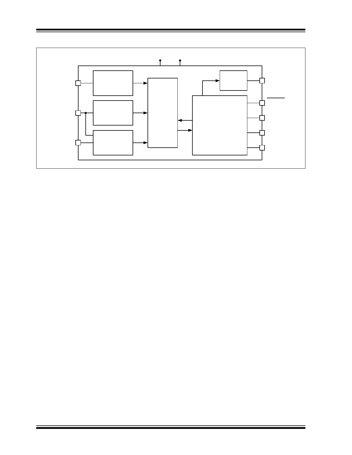
Device Block Diagram
Diff Current
Amplifier
V Buffer/
Divider
Digital Control
V
DD
GND
SENSE+
SENSE-
OUT
READ/INT
ADDR_SEL
11-bit or
14-bit
ADC
and
MUX
10-bit
DAC
SM_CLK
SM_DATA
Resistor
Decoder
RESERVED

2012-2016 Microchip Technology Inc.
DS20005293D-page 3
PAC1921
1.0
ELECTRICAL CHARACTERISTICS
1.1
Electrical Specifications
Absolute Maximum Ratings
(†)
V
DD
pin............................................................................................................................................................-0.3 to 6.0V
Voltage on SENSE- and SENSE+ pins............................................................................................................-0.3 to 42V
Voltage on ADDR_SEL pin .............................................................................................................................-0.3 to 2.6V
Voltage on any other pin to GND ....................................................................................................................-0.3 to 6.0V
Voltage between Sense pins (|(SENSE+ – SENSE-)|) ...............................................................................................40V
Input current to any pin except V
DD
......................................................................................................................±10 mA
Output short circuit current.............................................................................................................................. Continuous
Package Power Dissipation (
Note
) ...............................................................................................0.5W up to T
A
= +85°C
Junction to Ambient (
JA
)....................................................................................................................................+78°C/W
Operating Ambient Temperature Range .......................................................................................................-40 to +85°C
Storage Temperature Range.......................................................................................................................-55 to +150°C
ESD Rating - All pins - HBM ...................................................................................................................................2000V
† Notice: Stresses above those listed under “Absolute Maximum Ratings” may cause permanent damage to the device.
This is a stress rating only and functional operation of the device at those or any other conditions above those indicated
in the operation listings of this specification is not implied. Exposure above maximum rating conditions for extended
periods may affect device reliability.
Note:
The Package Power Dissipation specification assumes a recommended thermal via design consisting of a
2 x 2 matrix of 0.3 mm (12 mil) vias at 1.0 mm pitch connected to the ground plane with a 1.6 mm x 2.3 mm
thermal landing

PAC1921
DS20005293D-page 4
2012-2016 Microchip Technology Inc.
TABLE 1-1:
ELECTRICAL CHARACTERISTICS
Electrical Characteristics: Unless otherwise specified, maximum values are at T
A
= -40°C to +85°C, V
DD
= 3V to 5.5V,
V
BUS
= 0V to 32V; typical values are at T
A
= +25°C, V
DD
= 3.3V, V
BUS
= 24V, V
SENSE
= (SENSE+ – SENSE-) = 0V
Characteristic
Sym.
Min.
Typ.
Max.
Unit
Conditions
Power Supply
V
DD
Range
V
DD
3.0
—
5.5
V
V
DD
Integrate Current
I
DD
—
450
900
µA
Output unloaded
V
DD
Read Current
I
READ
—
300
450
µA
Output unloaded
V
DD
Sleep Current
I
SLEEP
—
3.5
15
µA
V
DD
Rise Rate
V
DD_RISE
0.05
—
1000
V/ms
0 to 3V in 60 ms
Analog Input Characteristics
Bus Voltage Range
V
BUS
0
—
32
V
Common-mode voltage on
SENSE pins, referenced to
ground
V
SENSE
Differential
Input Voltage Range
V
SENSE_DIF
0
—
100
mV
ADC Data Resolution
ADC_RES
—
—
14
bits
V
SENSE
LSB Step Size
V
SENSE_
LSB
—
6.1
—
µV
14-bit resolution
—
48.8
—
µV
11-bit resolution
V
BUS
LSB Step Size
V
BUS_
LSB
—
1.95
—
mV
14-bit resolution
—
15.6
—
mV
11-bit resolution
V
SENSE
Gain Accuracy
V
SENSE_ GAIN_ERR
—
±0.2
±0.4
%
Gain = 1
V
SENSE
Offset Accuracy,
Referenced to Input
V
SENSE_ OFFSET_ERR
—
±25
±100
µV
14-bit resolution
V
BUS
Gain Accuracy
V
BUS_GAIN_ERR
—
—
±0.4
%
Measured at ADC output,
Gain = 1
SENSE+, SENSE-
Pin Leakage
Current
I
SENSE +,
I
SENSE-
—
—
1.0
µA
V
BUS
= 24V, V
SENSE
= 0V
Sleep state
SENSE+, SENSE-
Pin Leakage Current
I
SENSE +,
I
SENSE-
—
—
1.0
µA
V
DD
= 0V
SENSE+ Pin Bias
Current
I
SENSE+_BIAS
—
34
—
µA
V
BUS
= 24V,
V
SENSE
= 100 mV
Integrate state,
Power measurement
SENSE- Pin Bias
Current
I
SENSE-_BIAS
—
—
1.0
µA
V
BUS
= 24V,
V
SENSE
= 0 to 100 mV
Integrate state

2012-2016 Microchip Technology Inc.
DS20005293D-page 5
PAC1921
DAC and OUT Amplifier Characteristics
Output Voltage
Swing
V
OUT
0
3.0
V
DD
-0.15
V
3V FSR maximum
equation in effect when V
DD
falls below 3.15V
Output Gain Error
OUT
GAIN_ERR
—
—
±0.2
%
Output Offset Error,
Referenced to
Output
OUT
OFFSET_ ERR
—
±3
±6
mV
3V FSR
Output Settling Time
t
SETTLE
—
—
42
µs
Output swing from 0V to
3.0V driving up to 50 pF
Output Load
C
OUT
—
—
50
pF
Output Current Drive
I
OUT
—
—
±3
mA
DC
OUT Short Circuit
I
OUT_SHORT
—
—
20
mA
Device cannot be
damaged when OUT pin is
short circuited to GND
OUT Power Supply
Rejection Ratio, DC,
Referenced to Input
OUT
PSRR_DC
—
69
—
dB
Integration and Read Timing
Time to First
Communications
t
INT_T
—
14.25
20
ms
Time after power-up before
ready to begin
communications and
measurement
Update Pulse
t
UPDATE
1.25
—
9.2
µs
READ/INT pin low pulse width
range to guarantee transfer of
digital value to DAC and not
enter Read state
Read Pulse
t
READ
9.8
—
—
µs
READ/INT pin minimum low
pulse width to guarantee
entry into Read state
Read State Time for
Auto-Sleep State
t
SLEEP
1.088
1.14
1.203
s
Transition From
Sleep State to Start
of Integration Period
t
SLEEP_TO_INT
—
—
86
µs
Transition From
Read State to Start
of Integration Period
t
READ_TO_INT
—
—
30
µs
TABLE 1-1:
ELECTRICAL CHARACTERISTICS (CONTINUED)
Electrical Characteristics: Unless otherwise specified, maximum values are at T
A
= -40°C to +85°C, V
DD
= 3V to 5.5V,
V
BUS
= 0V to 32V; typical values are at T
A
= +25°C, V
DD
= 3.3V, V
BUS
= 24V, V
SENSE
= (SENSE+ – SENSE-) = 0V
Characteristic
Sym.
Min.
Typ.
Max.
Unit
Conditions

PAC1921
DS20005293D-page 6
2012-2016 Microchip Technology Inc.
Digital I/O Pins (READ/INT, SMBus pins)
Output Low Voltage
V
OL
—
—
0.4
V
Sinking 8 mA
Input High Voltage
V
IH
2.0
—
—
V
Input Low Voltage
V
IL
—
—
0.8
V
Leakage Current
I
LEAK
-5
—
5
µA
Powered or unpowered,
T
A
< +85°C maximum
TABLE 1-2:
SMBUS MODULE SPECIFICATIONS
Electrical Characteristics: Unless otherwise specified, maximum values are at T
A
= -40°C to +85°C, V
DD
= 3V to 5.5V,
V
BUS
= 0V to 32V; typical values are at T
A
= +25°C, V
DD
= 3.3V, V
BUS
= 24V, V
SENSE
= (SENSE+ – SENSE-) = 0V
Characteristic
Sym.
Min.
Typ.
Max.
Units
Conditions
SMBus Interface
Input Capacitance
C
IN
—
4
10
pF
SMBus Timing
Clock Frequency
f
SMB
10
—
400
kHz
Spike Suppression
t
SP
0
—
50
ns
Pulse width of spikes that
must be suppressed by the
input filter
Bus Free Time
Stop to Start
t
BUF
1.3
—
—
µs
Start Setup Time
t
SU:STA
0.6
—
—
µs
Start Hold Time
t
HD:STA
0.6
—
—
µs
Stop Setup Time
t
SU:STO
0.6
—
—
µs
Data Hold Time
t
HD:DAT
0
—
—
µs
When transmitting to the
master
Data Hold Time
t
HD:DAT
0.3
—
—
µs
When receiving from the
master
Data Setup Time
t
SU:DAT
0.6
—
—
µs
Clock Low Period
t
LOW
1.3
—
—
µs
Clock High Period
t
HIGH
0.6
—
—
µs
Clock/Data Fall Time
t
FALL
—
—
300
ns
Minimum = 20 + 0.1 C
LOAD
ns
Clock/Data Rise Time
t
RISE
—
—
300
ns
Minimum = 20 + 0.1 C
LOAD
ns
Capacitive Load
C
LOAD
—
—
400
pF
Total per bus line
Time Out
t
TIMEOUT
25
—
35
ms
Disabled by default
Idle Reset
t
IDLE_RESET
350
—
—
µs
Disabled by default (see
Section 5.2 “SMBus
Timeout”
)
TABLE 1-1:
ELECTRICAL CHARACTERISTICS (CONTINUED)
Electrical Characteristics: Unless otherwise specified, maximum values are at T
A
= -40°C to +85°C, V
DD
= 3V to 5.5V,
V
BUS
= 0V to 32V; typical values are at T
A
= +25°C, V
DD
= 3.3V, V
BUS
= 24V, V
SENSE
= (SENSE+ – SENSE-) = 0V
Characteristic
Sym.
Min.
Typ.
Max.
Unit
Conditions
2012-2016 Microchip Technology Inc.
DS20005293D-page 7
PAC1921
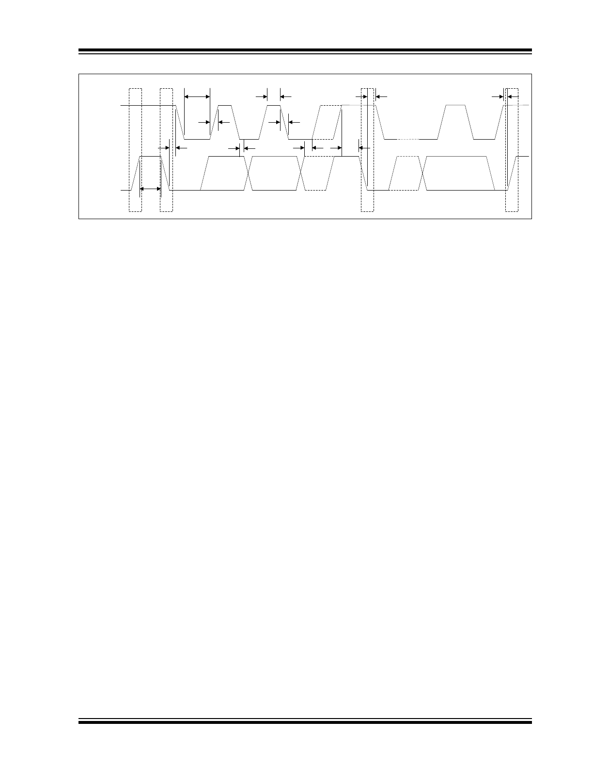
FIGURE 1-1:
SMBus Timing.
SMDATA
SMCLK
T
LOW
T
RISE
T
HIGH
T
FALL
T
BUF
T
HD:STA
P
S
S - Start Condition
P - Stop Condition
T
HD:DAT
T
SU:DA
T
T
SU:STA
T
HD:STA
P
T
SU:STO
S

PAC1921
DS20005293D-page 8
2012-2016 Microchip Technology Inc.
NOTES:
2012-2016 Microchip Technology Inc.
DS20005293D-page 9
PAC1921
2.0
TYPICAL OPERATING CURVES
Note: Unless otherwise specified, maximum values are at T
A
= -40°C to 85°C, V
DD
= 3V to 5.5V, V
BUS
= 0V to 32V;
typical values are at T
A
= 25°C, V
DD
= 3.3V, V
BUS
= 24V, V
SENSE
= (SENSE+ - SENSE-) = 0V
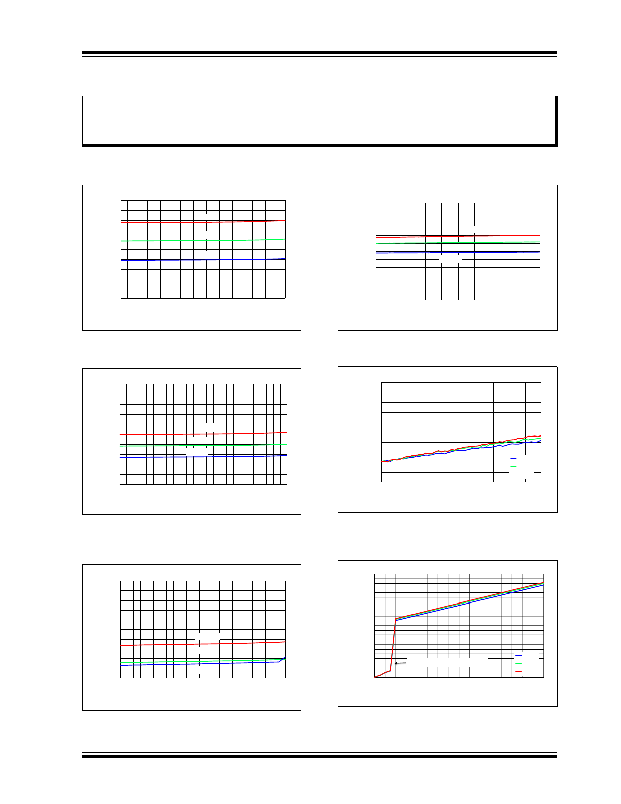
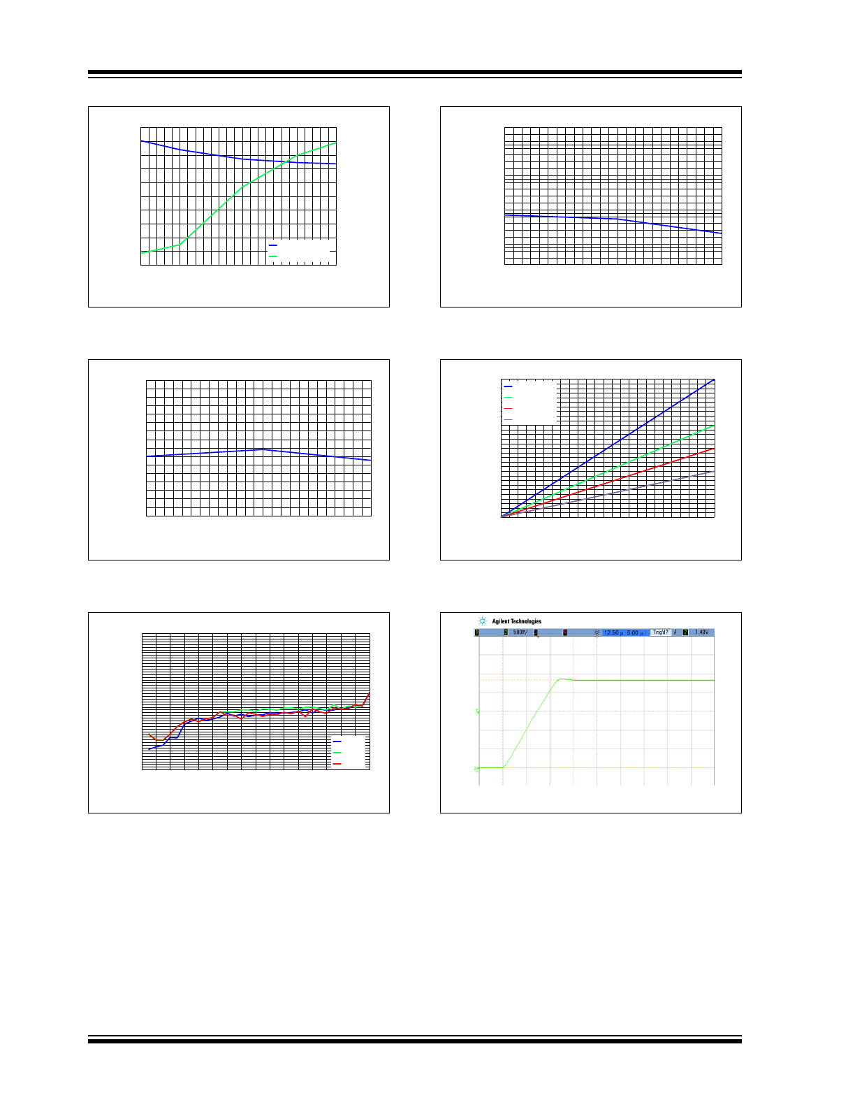
FIGURE 2-1:
Integrate State I
DD
vs. V
DD
(V
BUS
= 24V, V
SENSE
= 0V).
FIGURE 2-2:
Read State I
DD
vs. V
DD
(V
BUS
= 24, V
SENSE
= 0V).
FIGURE 2-3:
Sleep State I
DD
vs. V
DD
(V
BUS
= 24, V
SENSE
= 0V).
FIGURE 2-4:
I
SENSE+
Input Current vs.
V
SENSE
- Integrate State.
FIGURE 2-5:
I
SENSE-
Input Current vs.
V
SENSE
- Integrate State (V
BUS
= 24V, V
SENSE
=
100 mV).
FIGURE 2-6:
I
SENSE+
Input Current vs.
Common-Mode Voltage (V
BUS
) Integrate State
(V
DD
= 3.3V, V
SENSE
= 100 mV).
Note:
The graphs and tables provided following this note are a statistical summary based on a limited number of
samples and are provided for informational purposes only. The performance characteristics listed herein
are not tested or guaranteed. In some graphs or tables, the data presented may be outside the specified
operating range (e.g., outside specified power supply range) and therefore outside the warranted range.
300
320
340
360
380
400
420
440
460
480
500
3.0
3.5
4.0
4.5
5.0
5.5
I
DD
(
μ
A)
V
DD
(V)
+85
°C
+25
°C
-40
°C
200
220
240
260
280
300
320
340
360
380
400
3.0
3.5
4.0
4.5
5.0
5.5
I
DD
(
μ
A)
V
DD
(V)
+85
° C
+25
° C
-40
° C
0
2
4
6
8
10
12
14
16
18
20
3.0
3.5
4.0
4.5
5.0
5.5
I
DD
(
μ
A)
V
DD
(V)
+85
° C
+25
° C
-40
° C
32
33
34
35
36
37
38
0
20
40
60
80
100
I
SENSE+
(
μ
A)
V
SENSE
FSR (%)
+85
°C
+25
°C
-40
°C
0.00
0.10
0.20
0.30
0.40
0.50
0
20
40
60
80
100
I
SENSE
- (
μ
A)
V
SENSE
FSR (%)
-40°C
+25°C
+85°C
0
4
8
12
16
20
24
28
32
36
40
44
0
4
8
12
16
20
24
28
32
I
SENSE
+ (
μ
A)
V
BUS
(V)
-40°C
+25°C
+85°C
V
DD
= 3.3V Crossover Point
PAC1921
DS20005293D-page 10
2012-2016 Microchip Technology Inc.
FIGURE 2-7:
Current Sense Offset vs.
Temperature (V
BUS
= 24V, V
SENSE
= 100 mV).
FIGURE 2-8:
Current Sense Gain Error
vs. Temperature (V
BUS
= 24V, V
SENSE
= 98 mV).
FIGURE 2-9:
V
BUS
Voltage Measurement
Accuracy vs. Temperature (V
DD
= 3.3V, V
SENSE
= 98 mV).
FIGURE 2-10:
Current Sense Offset vs.
Temperature (V
BUS
= 32V, V
SENSE
= 98 mV).
FIGURE 2-11:
V
OUT
vs. V
SENSE
(V
DD
=
3.3V, V
BUS
= 24V).
FIGURE 2-12:
DAC Setting Time.
-30
-25
-20
-15
-10
-5
0
5
10
0.0
0.2
0.4
0.6
0.8
1.0
1.2
1.4
1.6
1.8
2.0
-40
-25
-10
5
20
35
50
65
80
Input V
OFFSET
(μ
V)
Output V
OFFSET
(mV)
Temperature (
°C)
Output Offset
Input Offset
-0.40
-0.30
-0.20
-0.10
0.00
0.10
0.20
0.30
0.40
-40
-15
10
35
60
85
Gain Error (%
)
Temperature (
°C)
-0.5
-0.4
-0.3
-0.2
-0.1
0.0
0.1
0.2
0.3
0.4
0.5
0
4
8
12
16
20
24
28
32
V
BUS
Error (%
)
V
BUS
(V)
-40°C
+25°C
+85°C
-0.20
-0.15
-0.10
-0.05
0.00
0.05
0.10
0.15
0.20
-40
-15
10
35
60
85
Error (%
)
Temperature (
°C)
0
500
1,000
1,500
2,000
2,500
3,000
0.000
0.020
0.040
0.060
0.080
0.100
V
OUT
(mV)
V
SENSE
(V)
3V Range
2V Range
1.5V Range
1V Range