
2016 Microchip Technology Inc.
DS20005685A-page 1
MIC2915X/30X/50X/75X
Features
• High Current Capability:
- MIC29150/29151/29152/29153: 1.5A
- MIC29300/29301/29302/29303: 3A
- MIC29500/29501/29502/29503: 5A
- MIC29751/29752: 7.5A
• Low Dropout Voltage
• Low Ground Current
• Accurate 1% Guaranteed Tolerance
• Extremely Fast Transient Response
• Reverse-Battery and “Load Dump” Protection
• Zero-Current Shutdown Mode (5-Pin Versions)
• Error Flag Signals Output Out-of-Regulation
(5-Pin Versions)
• Also Characterized for Smaller Loads with
Industry-Leading Performance Specifications
• Fixed-Voltage and Adjustable Versions
Applications
• Battery-Powered Equipment
• High-Efficiency Green Computer Systems
• Automotive Electronics
• High-Efficiency Linear Power Supplies
• High-Efficiency Post-Regulator for Switching
Supply
General Description
The MIC2915x/2930x/2950x/2975x are high current,
high accuracy, low dropout voltage regulators. Using
Microchip’s proprietary Super βeta PNP process with a
PNP pass element, these regulators feature 350 mV to
425 mV (full load) typical dropout voltages and very low
ground current. Designed for high current loads, these
devices also find applications in lower current,
extremely low dropout-critical systems, where their tiny
dropout voltage and ground current values are
important attributes.
The MIC2915x/2930x/2950x/2975x are fully protected
against overcurrent faults, reversed input polarity,
reversed lead insertion, overtemperature operation,
and positive and negative transient voltage spikes. Five
pin fixed-voltage versions feature logic level ON/OFF
control and an error flag that signals whenever the
output falls out of regulation. Flagged states include
low input voltage (dropout), output current limit,
overtemperature shutdown, and extremely high voltage
spikes on the input.
On the MIC29xx1 and MIC29xx2, the ENABLE pin may
be tied to V
IN
if it is not required for ON/OFF control.
The MIC2915x/2930x/2950x are available in 3-pin and
5-pin TO-220 and surface mount TO-263 (D
2
Pak)
packages. The MIC2975x 7.5A regulators are available
in a 5-pin TO-247 package. The 1.5A, adjustable output
MIC29152 is available in a 5-pin power D-Pak
(TO-252) package.
For applications with input voltage 6V or below, see
MIC37xxx LDOs.
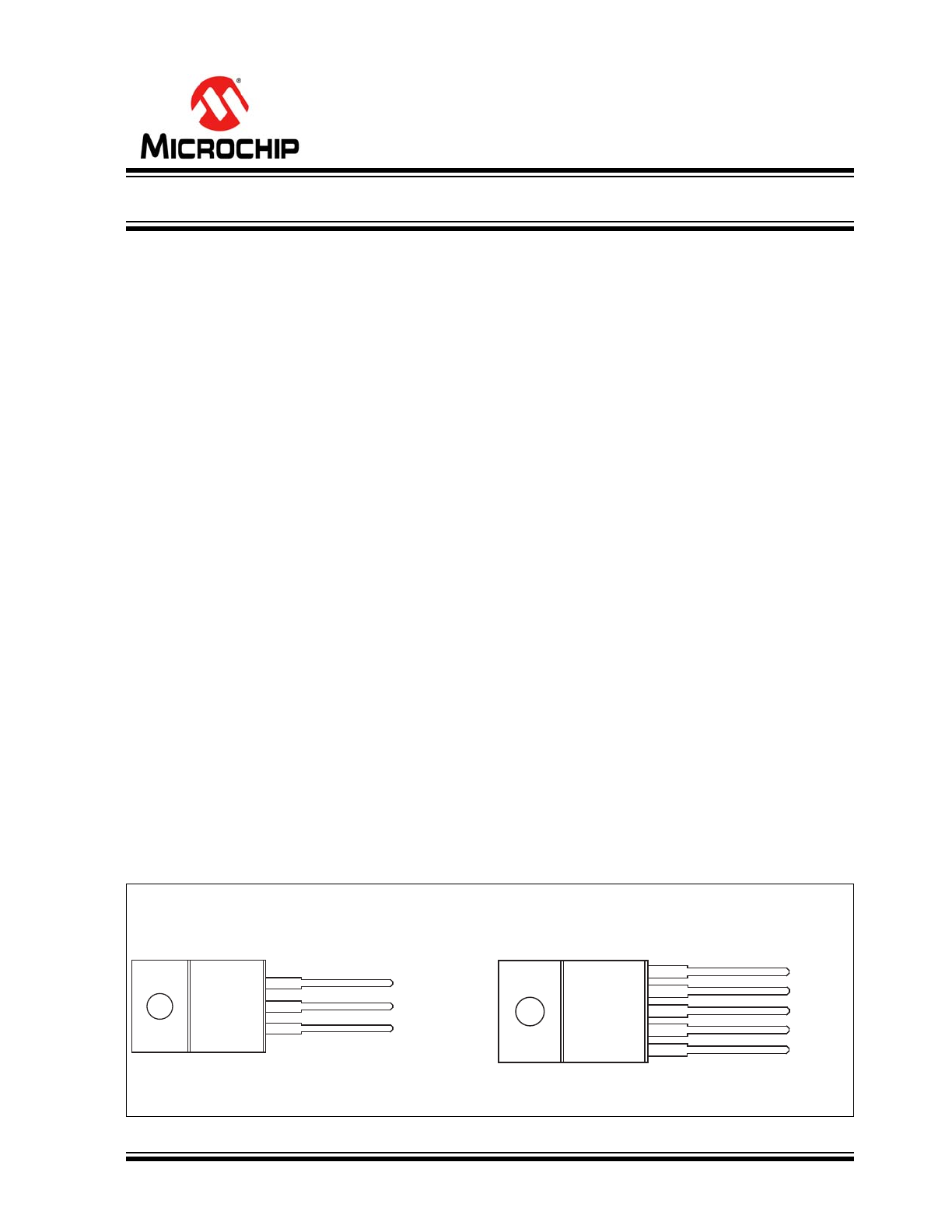
Package Types
MIC29150/300/500
3-Lead TO-220 (T)
(Top View)
TA
B
3 OUT
2 GND
1 IN
TA
B
3 GND
4 OUT
5 FLG
2 IN
1 EN
MIC29151/301/501/751
5-Lead TO-220 Fixed Voltage (T)
(Top View)
High-Current Low Dropout Regulators
MIC2915X/30X/50X/75X
DS20005685A-page 2
2016 Microchip Technology Inc.
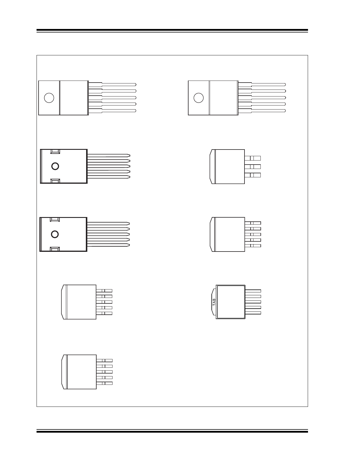
Package Types (Continued)
MIC29152/302/502
5-Lead TO-220 Adjustable Voltage (T)
(Top View)
TA
B
3 GND
4 OUT
5 ADJ
2 IN
1 EN
TA
B
3 GND
4 OUT
5 ADJ
2 IN
1 FLG
MIC29153/303/503
5-Lead TO-220 Adjustable with Flag (T)
(Top View)
1
2
3
4
5
EN
IN
GND
OUT
FLG
MIC29751
5-Lead TO-247 Fixed Voltage (WT)
(Top View)
1
2
3
4
5
EN
IN
GND
OUT
ADJ
MIC29752
5-Lead TO-247 Adjustable Voltage (WT)
(Top View)
TA
B
3 OUT
2 GND
1 IN
MIC29150/300
3-Lead TO-263 (D
2
Pak) (UT)
(Top View)
TA
B
5 FLG
4 OUT
3 GND
2 IN
1 EN
MIC29151/301/501
5-Lead TO-263 (D
2
Pak) Fixed Voltage (U)
(Top View)
TA
B
5 ADJ
4 OUT
3 GND
2 IN
1 EN
MIC29302/502
5-Lead TO-263 (D
2
Pak) Adj. Voltage (U)
(Top View)
TA
B
5 ADJ
4 OUT
3 GND
2 IN
1 FLG
MIC29153/303/503
5-Lead TO-263 (D
2
Pak) Adj. with Flag (U)
(Top View)
1 EN
2 IN
3 GND
4 OUT
5 ADJ
MIC29152
5-Lead TO-252 (D-Pak) Adjustable Voltage (D)
(Top View)
2016 Microchip Technology Inc.
DS20005685A-page 3
MIC2915X/30X/50X/75X
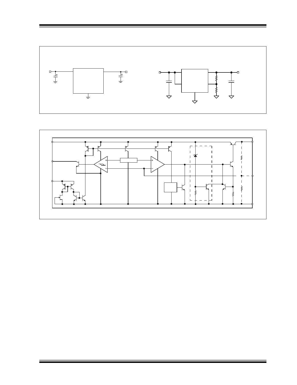
Typical Application Circuits
Functional Diagram
MIC29300-3.3
10μF Tantalum
3.3V @ 3A
IN
OUT
GND
C
IN
5V
OUT
IN
ADJ
GND
EN
10μF Tantalum
*R1
ȍ
*R2
ȍ
2.5VOUT@1.5A
MIC29152WD
3.3V
IN
C
IN
+
MIC29300
Fixed Output Version
MIC29152
Adjustable Output Version
* See Minimum Load Current Section
1.180V
1.240V
REFERENCE
IN
FLAG
EN
THERMAL
SHUT-
DOWN
OUT
ADJ†
GND
R1*
R2*
O.V.
I
LIMIT
32V
* FEEDBACK NETWORK IN FIXED VERSIONS ONLY
† ADJUSTABLE VERSION ONLY

MIC2915X/30X/50X/75X
DS20005685A-page 4
2016 Microchip Technology Inc.
1.0
ELECTRICAL CHARACTERISTICS
Absolute Maximum Ratings † (
Note 1
)
Input Supply Voltage (V
IN
) (
Note 1
)............................................................................................................. –20V to +60V
Enable Input Voltage (V
EN
) ........................................................................................................................... –0.3V to V
IN
Power Dissipation...................................................................................................................................Internally Limited
ESD Rating ............................................................................................................................................................
Note 2
Operating Ratings‡
Maximum Operating Input Voltage ............................................................................................................................+26V
†
Notice: Stresses above those listed under “Absolute Maximum Ratings” may cause permanent damage to the device.
This is a stress rating only and functional operation of the device at those or any other conditions above those indicated
in the operational sections of this specification is not intended. Exposure to maximum rating conditions for extended
periods may affect device reliability.
‡ Notice:
The device is not guaranteed to function outside its operating ratings.
Note 1:
Maximum positive supply voltage of 60V must be of limited duration (<100 ms) and duty cycle (≤1%). The
maximum continuous supply voltage is 26V. Exceeding the absolute maximum rating may damage the
device.
2:
Devices are ESD sensitive. Handling precautions recommended.
2016 Microchip Technology Inc.
DS20005685A-page 5
MIC2915X/30X/50X/75X
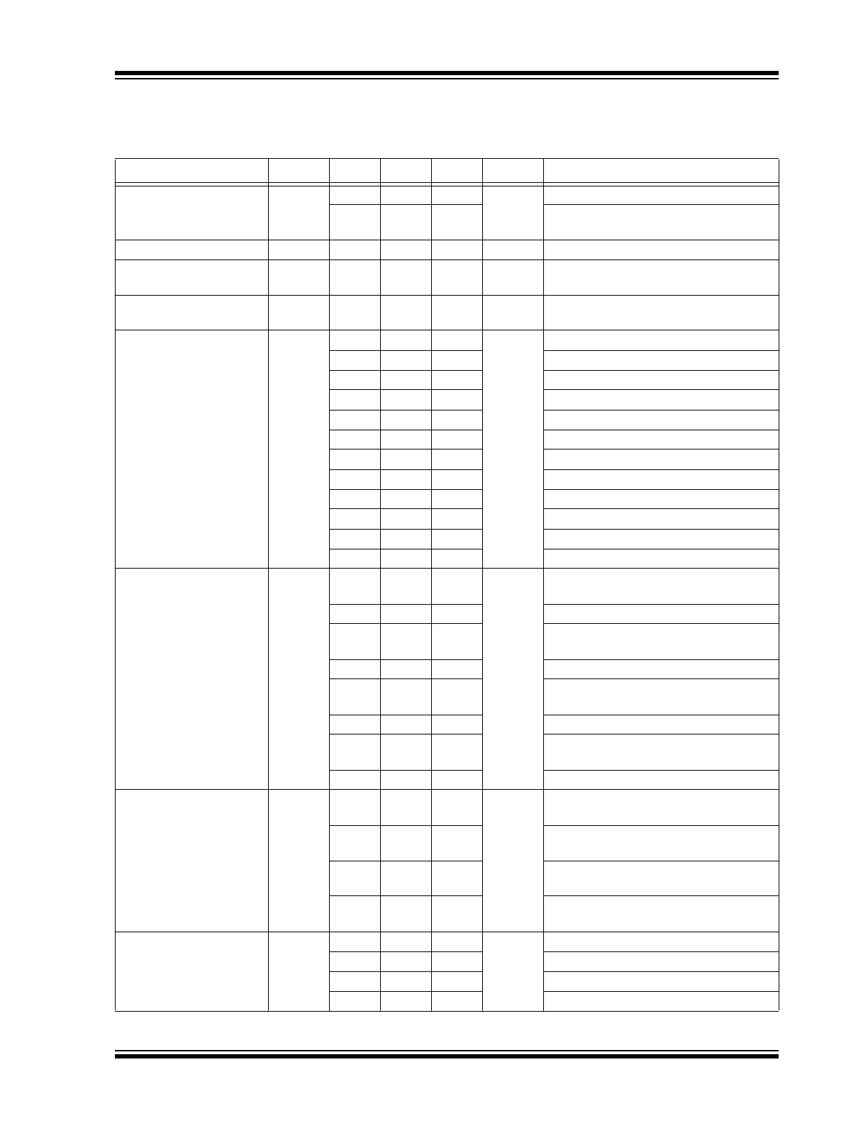
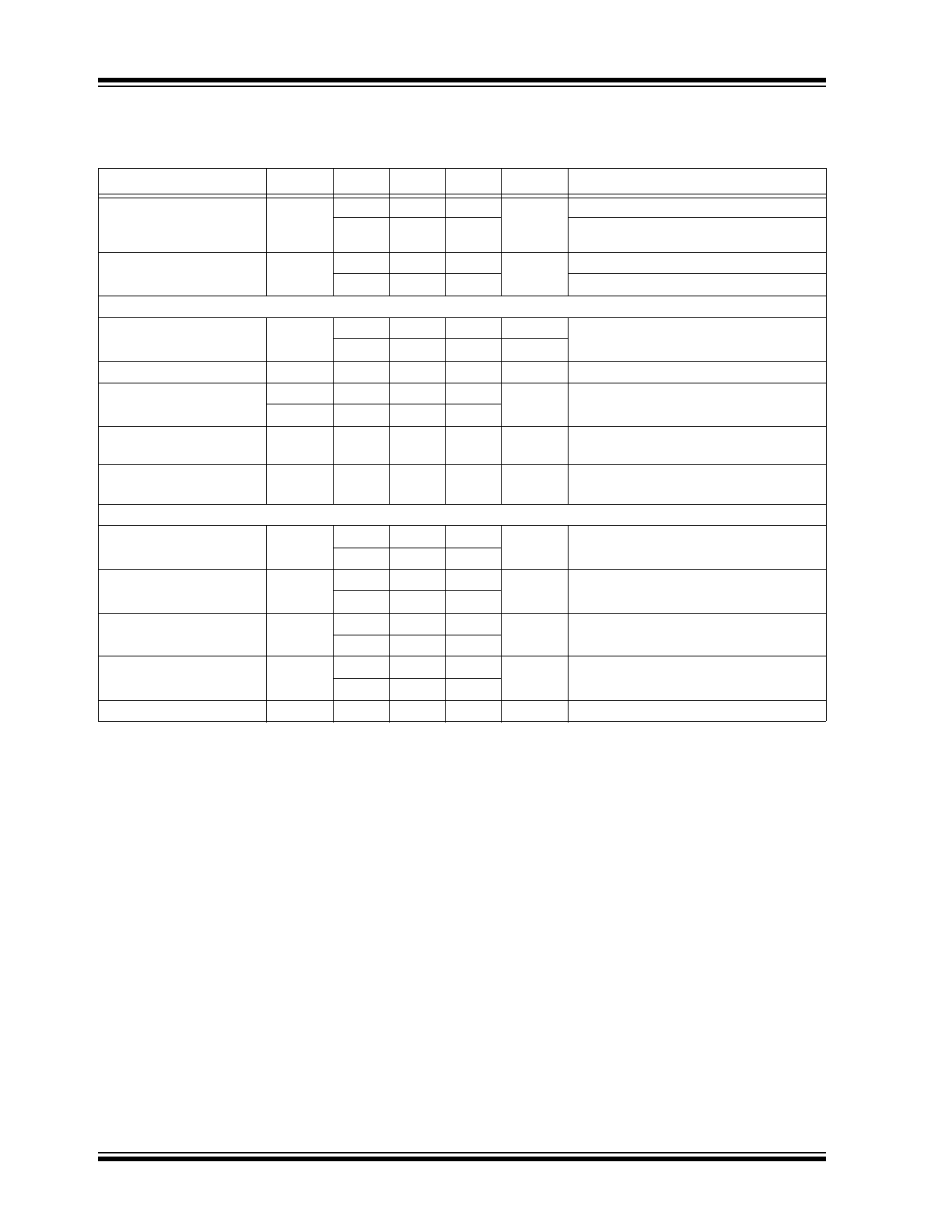
TABLE 1-1:
ELECTRICAL CHARACTERISTICS (
Note 1
,
Note 2
)
Electrical Characteristics:
V
IN
= V
OUT
+ 1V; I
OUT
= 10 mA; T
J
= +25°C. Bold values indicate –40°C ≤ T
J
≤ +125°C,
unless noted.
Parameter
Symbol
Min.
Typ.
Max.
Units
Conditions
Output Voltage
V
OUT
–1
—
1
%
I
OUT
= 10 mA
–2
—
2
10 mA ≤ I
OUT
≤ I
FL
, (V
OUT
+ 1V) ≤ V
IN
≤26V (
Note 3
)
Line Regulation
—
0.06
0.5
%
I
OUT
= 10 mA, (V
OUT
+ 1V) ≤ V
IN
≤ 26V
Load Regulation
—
0.2
1
%
V
IN
= V
OUT
+ 1V, 10 mA ≤ I
OUT
≤ 1.5A
(
Note 3
,
Note 4
)
∆V
O
/∆T
—
20
100
ppm/°C
Output Voltage (
Note 4
)
Temperature Coefficient
Dropout Voltage
∆V
OUT
= –1% (
Note 5
)
—
80
200
mV
MIC2915x I
OUT
= 100 mA
—
220
—
MIC2915x I
OUT
= 750 mA
—
350
600
MIC2915x I
OUT
= 1.5A
—
80
175
MIC2930x I
OUT
= 100 mA
—
250
—
MIC2930x I
OUT
= 1.5A
—
370
600
MIC2930x I
OUT
= 3A
—
125
250
MIC2950x I
OUT
= 250 mA
—
250
—
MIC2950x I
OUT
= 2.5A
—
370
600
MIC2950x I
OUT
= 5A
—
80
200
MIC2975x I
OUT
= 250 mA
—
270
—
MIC2975x I
OUT
= 4A
—
425
750
MIC2975x I
OUT
= 7.5A
Ground Current (
Note 6
)
I
GND
—
8
20
mA
MIC2915x I
OUT
= 750 mA,
V
IN
= V
OUT
+ 1V
—
22
—
MIC2915x I
OUT
= 1.5A
—
10
35
MIC2930x I
OUT
= 1.5A,
V
IN
= V
OUT
+ 1V
—
37
—
MIC2930x I
OUT
= 3A
—
15
50
MIC2950x I
OUT
= 2.5A,
V
IN
= V
OUT
+ 1V
—
70
—
MIC2950x I
OUT
= 5A
—
35
75
MIC2975x I
OUT
= 4A,
V
IN
= V
OUT
+ 1V
120
—
MIC2975x I
OUT
= 7.5A
Ground Pin Current at
Dropout
I
GRNDDO
—
0.9
—
mA
MIC2915x, V
IN
= 0.5V less than
specified V
OUT
× I
OUT
= 10 mA
—
1.7
—
MIC2930x, V
IN
= 0.5V less than
specified V
OUT
× I
OUT
= 10 mA
—
2.1
—
MIC2950x, V
IN
= 0.5V less than
specified V
OUT
× I
OUT
= 10 mA
—
3.1
—
MIC2975x, V
IN
= 0.5V less than
specified V
OUT
× I
OUT
= 10 mA
Current Limit
I
LIM
—
2.1
3.5
A
MIC2915x, V
OUT
= 0V, (
Note 7
)
—
4.5
5.0
MIC2930x, V
OUT
= 0V, (
Note 7
)
—
7.5
10.0
MIC2950x, V
OUT
= 0V, (
Note 7
)
—
9.5
15.0
MIC2975x, V
OUT
= 0V, (
Note 7
)
MIC2915X/30X/50X/75X
DS20005685A-page 6
2016 Microchip Technology Inc.
e
n
, Output Noise Voltage
(10 Hz to 100 kHz)
I
L
= 100 mA
—
400
—
µV
RMS
C
L
= 10 µF
—
260
—
C
L
= 33 µF
Ground Current in
Shutdown
—
2
10
µA
MIC29150/1/2/3 only
—
—
30
V
EN
= 0.4V
Reference - MIC29xx2/MIC29xx3
Reference Voltage
1.228
1.240
1.252
V
—
1.215
—
1.265
V
MAX
Reference Voltage
1.203
—
1.277
V
Note 8
Adjust Pin Bias Current
—
40
80
nA
—
—
—
120
Reference Voltage
Temperature Coefficient
—
20
—
ppm/°C
Note 9
Adjust Pin Bias Current
Temperature Coefficient
—
0.1
—
nA/°C
—
Flag Output (Error Comparator) - MIC29xx1/29xx3
Output Leakage Current
—
0.01
1.00
µA
V
OH
= 26V
—
—
2.00
Output Low Voltage
V
OL
—
220
300
mV
Device set for 5V, V
IN
= 4.5V
I
OL
= 250 µA
—
—
400
Upper Threshold Voltage
40
60
—
mV
Device set for 5V, (
Note 10
)
25
—
—
Lower Threshold Voltage
—
75
95
mV
Device set for 5V, (
Note 10
)
—
—
140
Hysteresis
—
15
—
mV
Device set for 5V, (
Note 10
)
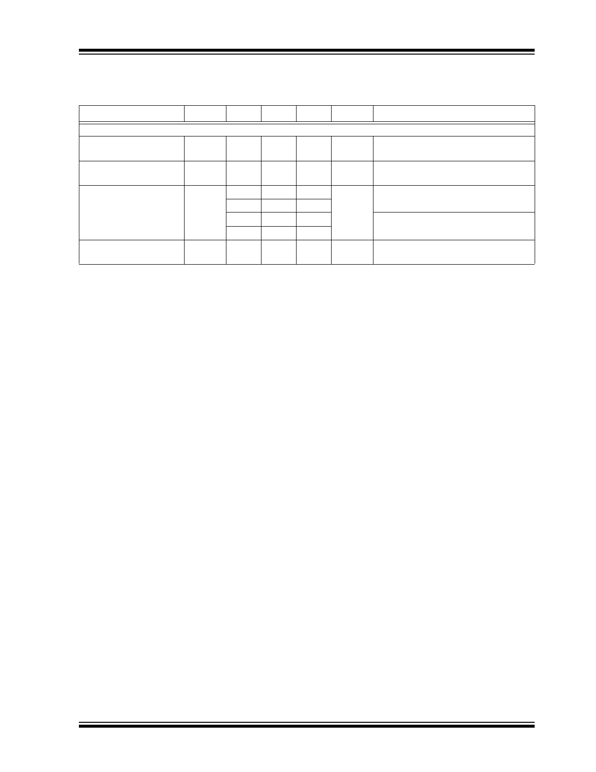
TABLE 1-1:
ELECTRICAL CHARACTERISTICS (
Note 1
,
Note 2
) (CONTINUED)
Electrical Characteristics:
V
IN
= V
OUT
+ 1V; I
OUT
= 10 mA; T
J
= +25°C. Bold values indicate –40°C ≤ T
J
≤ +125°C,
unless noted.
Parameter
Symbol
Min.
Typ.
Max.
Units
Conditions
2016 Microchip Technology Inc.
DS20005685A-page 7
MIC2915X/30X/50X/75X
ENABLE Input - MIC29xx1/MIC29xx2
Input Logic Voltage Low
(OFF)
—
—
0.8
V
—
Input Logic Voltage High
(ON)
2.4
—
—
V
—
Enable Pin Input Current
—
100
600
µA
V
EN
= 26V
—
—
750
0.7
—
2
V
EN
= 0.8V
—
—
4
Regulator Output Current
in Shutdown
—
10
500
µA
V
EN
≤ 0.8V and V
IN
≤ 26V, V
OUT
= 0.
Note 1:
Specification for packaged product only.
2:
When used in dual supply systems where the regulator load is returned to a negative supply, the output
voltage must be diode clamped to ground.
3:
Full load current (I
FL
) is defined as 1.5A for the MIC2915x, 3A for the MIC2930x, 5A for the MIC2950x,
and 7.5A for the MIC2975x families.
4:
Output voltage temperature coefficient is defined as the worst case voltage change divided by the total
temperature range.
5:
Dropout voltage is defined as the input-to-output differential when the output voltage drops to 99% of its
normal value with V
OUT
+ 1V applied to V
IN
.
6:
Ground pin current is the regulator quiescent current. The total current drawn from the source is the sum
of the load current plus the ground pin current.
7:
V
IN
= V
OUT
(nominal) + 1V. For example, use V
IN
= 4.3V for a 3.3V regulator or use 6V for a 5V regulator.
Employ pulse-testing procedures to pin current.
8:
V
REF
≤ V
OUT
≤ (V
IN
– 1V), 2.3V ≤ V
IN
≤ 26V, 10 mA < I
L
≤ I
FL
, T
J
≤ T
JMAX
.
9:
Thermal regulation is defined as the change in output voltage at a time T after a change in power dissipa-
tion is applied, excluding load or line regulation effects. Specifications are for a 200 mA load pulse at V
IN
=
20V (a 4W pulse) for T = 10 ms.
10:
Comparator thresholds are expressed in terms of a voltage differential at the adjust terminal below the
nominal reference voltage measured at 6V input. To express these thresholds in terms of output voltage
change, multiply by the error amplifier gain = V
OUT
/V
REF
= (R1 + R2)/R2. For example, at a programmed
output voltage of 5V, the error output is guaranteed to go low when the output drops by 95 mV x
5V/1.240V = 384 mV. Thresholds remain constant as a percent of V
OUT
as V
OUT
is varied, with the drop-
out warning occurring at typically 5% below nominal, 7.7% guaranteed.
TABLE 1-1:
ELECTRICAL CHARACTERISTICS (
Note 1
,
Note 2
) (CONTINUED)
Electrical Characteristics:
V
IN
= V
OUT
+ 1V; I
OUT
= 10 mA; T
J
= +25°C. Bold values indicate –40°C ≤ T
J
≤ +125°C,
unless noted.
Parameter
Symbol
Min.
Typ.
Max.
Units
Conditions
MIC2915X/30X/50X/75X
DS20005685A-page 8
2016 Microchip Technology Inc.
TEMPERATURE SPECIFICATIONS (
Note 1
)
Parameters
Sym.
Min.
Typ.
Max.
Units
Conditions
Temperature Ranges
Storage Temperature Range
T
S
–65
—
+150
°C
—
Operating Junction Temperature
T
J
–40
—
+125
°C
—
Lead Temperature
—
—
—
+260
°C
Soldering, 5 sec.
Package Thermal Resistance
Thermal Resistance TO-220
θ
JC
—
2
—
°C/W
—
Thermal Resistance TO-263
θ
JC
—
2
—
°C/W
—
Thermal Resistance TO-247
θ
JC
—
1.5
—
°C/W
—
Thermal Resistance TO-252
θ
JC
—
3
—
°C/W
—
Thermal Resistance TO-252
θ
JA
—
56
—
°C/W
—
Note 1:
The maximum allowable power dissipation is a function of ambient temperature, the maximum allowable
junction temperature and the thermal resistance from junction to air (i.e., T
A
, T
J
,
JA
). Exceeding the
maximum allowable power dissipation will cause the device operating junction temperature to exceed the
maximum +125°C rating. Sustained junction temperatures above +125°C can impact the device reliability.
2016 Microchip Technology Inc.
DS20005685A-page 9
MIC2915X/30X/50X/75X
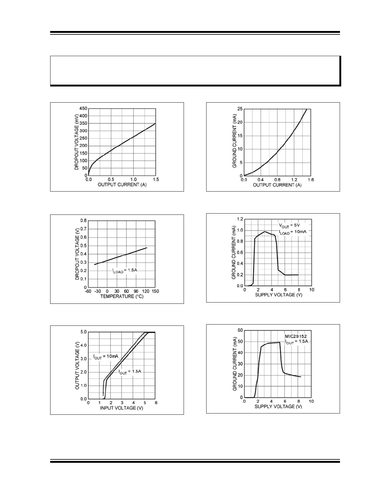
2.0
TYPICAL PERFORMANCE CURVES
FIGURE 2-1:
MIC2915x Dropout Voltage
vs. Output Current.
FIGURE 2-2:
MIC2915x Dropout Voltage
vs. Temperature.
FIGURE 2-3:
MIC29150-5.0 Dropout
Characteristics.
FIGURE 2-4:
MIC2915x Ground Current
vs. Output Current.
FIGURE 2-5:
MIC2915x Ground Current
vs. Supply Voltage.
FIGURE 2-6:
MIC2915x Ground Current
vs. Supply Voltage.
Note:
The graphs and tables provided following this note are a statistical summary based on a limited number of
samples and are provided for informational purposes only. The performance characteristics listed herein
are not tested or guaranteed. In some graphs or tables, the data presented may be outside the specified
operating range (e.g., outside specified power supply range) and therefore outside the warranted range.
MIC2915X/30X/50X/75X
DS20005685A-page 10
2016 Microchip Technology Inc.
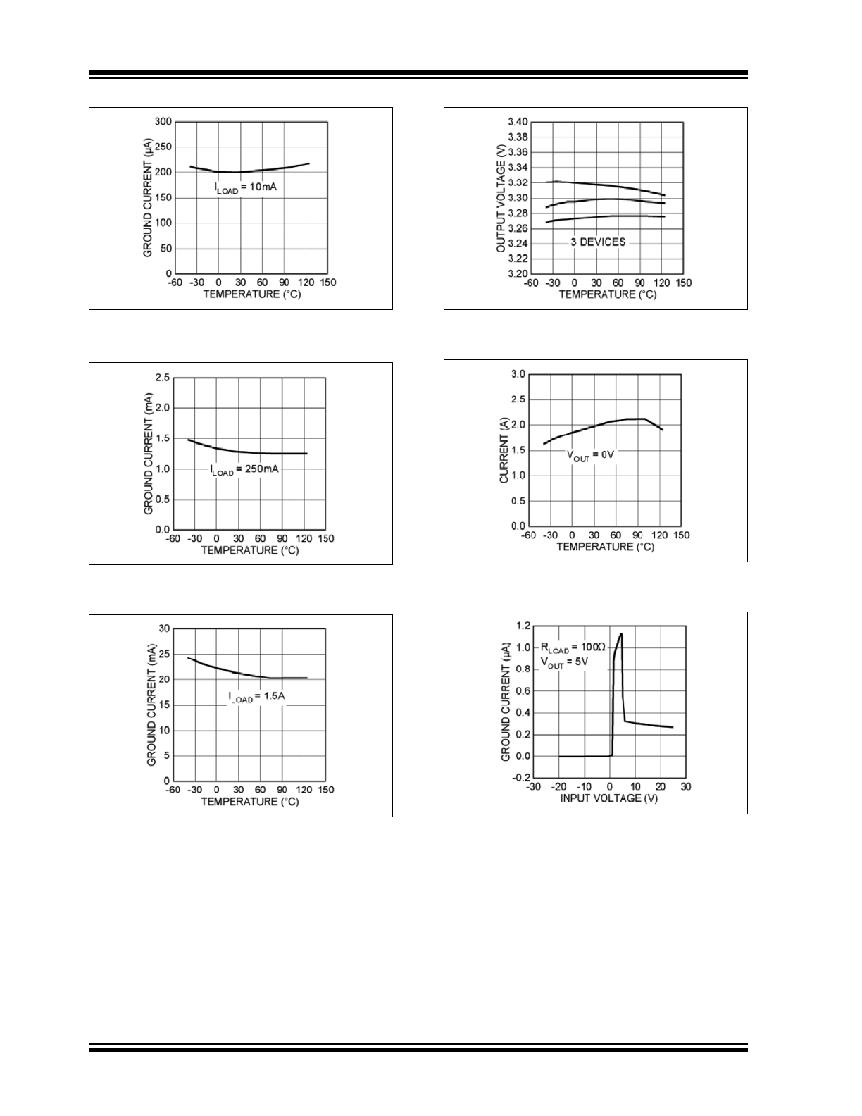
FIGURE 2-7:
MIC2915x Ground Current
vs. Temperature.
FIGURE 2-8:
MIC2915x Ground Current
vs. Temperature.
FIGURE 2-9:
MIC2915x Ground Current
vs. Temperature.
FIGURE 2-10:
MIC29150-3.3 Output
Voltage vs. Temperature.
FIGURE 2-11:
MIC29150-3.3 Short-Circuit
Current vs. Temperature.
FIGURE 2-12:
MIC2915x Ground Current
vs. Input Voltage.