
© 2011 Microchip Technology Inc.
DS40151E-page 1
HCS512
FEATURES
Security
• Secure storage of Manufacturer’s Code
• Secure storage of transmitter’s keys
• Up to four transmitters can be learned
• K
EE
L
OQ®
code hopping technology
• Normal and secure learning mechanisms
Operating
• 4.0V – 6.0V operation
• 4 MHz external RC oscillator
• Learning indication on LRNOUT
• Auto baud rate detection
• Power saving SLEEP mode
Other
• Stand-alone decoder
• On-chip EEPROM for transmitter storage
• Four binary function outputs–15 functions
• 18-pin DIP/SOIC package
Typical Applications
• Automotive remote entry systems
• Automotive alarm systems
• Automotive immobilizers
• Gate and garage openers
• Electronic door locks
• Identity tokens
• Burglar alarm systems
Compatible Encoders
All K
EE
L
OQ
encoders and transponders configured for
the following setting:
• PWM modulation format (1/3-2/3)
• T
E
in the range from 100
μs to 400 μs
• 10 x T
E
Header
• 28-bit Serial Number
• 16-bit Synchronization counter
• Discrimination bits equal to Serial Number 8 LSbs
• 66- to 69-bit length code word.
DESCRIPTION
The Microchip Technology Inc. HCS512 is a code hop-
ping decoder designed for secure Remote Keyless
Entry (RKE) systems. The HCS512 utilizes the pat-
ented K
EE
L
OQ
code hopping system and high security
learning mechanisms to make this a canned solution
when used with the HCS encoders to implement a uni-
directional remote keyless entry system.
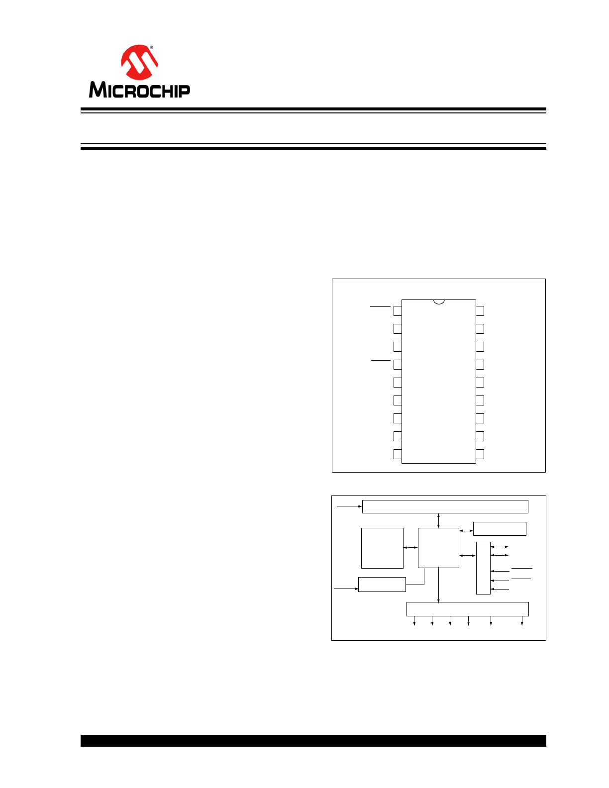
PACKAGE TYPE
BLOCK DIAGRAM
The Manufacturer’s Code, transmitter keys, and syn-
chronization information are stored in protected on-
chip EEPROM. The HCS512 uses the DATA and CLK
inputs to load the Manufacturer’s Code which cannot
be read out of the device.
HCS512
PDIP, SOIC
1
2
3
4
5
6
7
8
9
LRNIN
LRNOUT
NC
MCLR
GND
S0
S1
S2
S3
18
17
16
15
14
13
12
11
10
RFIN
NC
OSCIN
OSC
OUT
V
DD
DATA
CLK
SLEEP
V
LOW
S0
S1
S3
S2
V
LOW
Reception Register
EEPROM
CONTROL
DECRYPTOR
OUTPUT
RFIN
OSCILLATOR
OSCIN
CONTROL
LRNOUT
DATA
CLK
LRNIN
MCLR
SLEEP
K
EE
L
OQ®
Code Hopping Decoder

HCS512
DS40151E-page 2
© 2011 Microchip Technology Inc.
The HCS512 operates over a wide voltage range of
3.0 volts to 6.0 volts. The decoder employs automatic
baud rate detection which allows it to compensate for
wide variations in transmitter data rate. The decoder
contains sophisticated error checking algorithms to
ensure only valid codes are accepted.
1.0
SYSTEM OVERVIEW
Key Terms
The following is a list of key terms used throughout this
data sheet. For additional information on K
EE
L
OQ
and
Code Hopping, refer to Technical Brief 3 (TB003).
• RKE - Remote Keyless Entry
• Button Status - Indicates what button input(s)
activated the transmission. Encompasses the 4
button status bits S3, S2, S1 and S0 (Figure 8-2).
• Code Hopping - A method by which a code,
viewed externally to the system, appears to
change unpredictably each time it is transmitted.
• Code word - A block of data that is repeatedly
transmitted upon button activation (Figure 8-1).
• Transmission - A data stream consisting of
repeating code words (Figure 8-1).
• Crypt key - A unique and secret 64-bit number
used to encrypt and decrypt data. In a symmetri-
cal block cipher such as the K
EE
L
OQ
algorithm,
the encryption and decryption keys are equal and
will therefore be referred to generally as the crypt
key.
• Encoder - A device that generates and encodes
data.
• Encryption Algorithm - A recipe whereby data is
scrambled using a crypt key. The data can only be
interpreted by the respective decryption algorithm
using the same crypt key.
• Decoder - A device that decodes data received
from an encoder.
• Decryption algorithm - A recipe whereby data
scrambled by an encryption algorithm can be
unscrambled using the same crypt key.
• Learn – Learning involves the receiver calculating
the transmitter’s appropriate crypt key, decrypting
the received hopping code and storing the serial
number, synchronization counter value and crypt
key in EEPROM. The K
EE
L
OQ
product family facil-
itates several learning strategies to be imple-
mented on the decoder. The following are
examples of what can be done.
- Simple Learning
The receiver uses a fixed crypt key, common
to all components of all systems by the same
manufacturer, to decrypt the received code
word’s encrypted portion.
- Normal Learning
The receiver uses information transmitted
during normal operation to derive the crypt
key and decrypt the received code word’s
encrypted portion.
- Secure Learn
The transmitter is activated through a special
button combination to transmit a stored 60-bit
seed value used to generate the transmitter’s
crypt key. The receiver uses this seed value
to derive the same crypt key and decrypt the
received code word’s encrypted portion.
• Manufacturer’s code – A unique and secret 64-
bit number used to generate unique encoder crypt
keys. Each encoder is programmed with a crypt
key that is a function of the manufacturer’s code.
Each decoder is programmed with the manufac-
turer code itself.
1.1
HCS Encoder Overview
The HCS encoders have a small EEPROM array which
must be loaded with several parameters before use.
The most important of these values are:
• A crypt key that is generated at the time of pro-
duction
• A 16-bit synchronization counter value
• A 28-bit serial number which is meant to be
unique for every encoder
The manufacturer programs the serial number for each
encoder at the time of production, while the ‘Key Gen-
eration Algorithm’ generates the crypt key (Figure 1-1).
Inputs to the key generation algorithm typically consist
of the encoder’s serial number and a 64-bit manufac-
turer’s code, which the manufacturer creates.
Note:
The manufacturer code is a pivotal part of
the system’s overall security. Conse-
quently, all possible precautions must be
taken and maintained for this code.
© 2011 Microchip Technology Inc.
DS40151E-page 3
HCS512
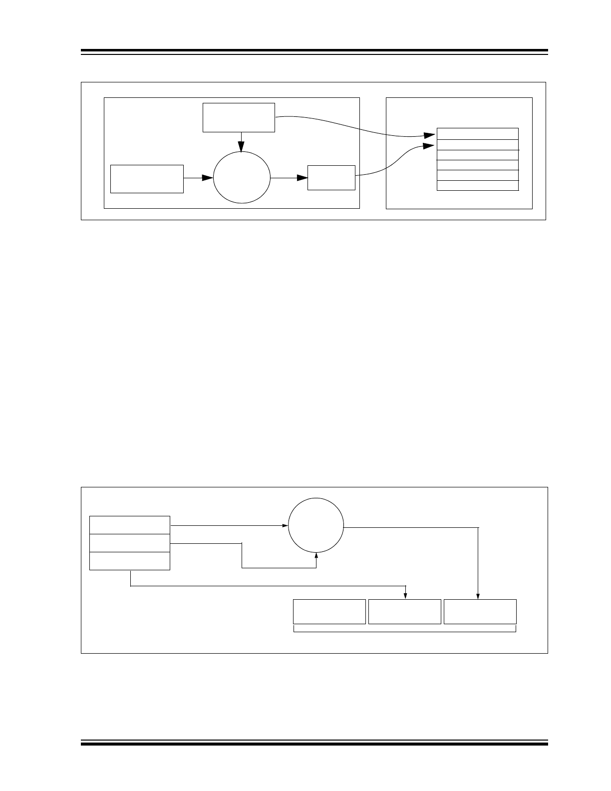
FIGURE 1-1:
CREATION AND STORAGE OF CRYPT KEY DURING PRODUCTION
The 16-bit synchronization counter is the basis behind
the transmitted code word changing for each transmis-
sion; it increments each time a button is pressed. Due
to the code hopping algorithm’s complexity, each incre-
ment of the synchronization value results in greater
than 50% of the bits changing in the transmitted code
word.
Figure 1-2 shows how the key values in EEPROM are
used in the encoder. Once the encoder detects a button
press, it reads the button inputs and updates the syn-
chronization counter. The synchronization counter and
crypt key are input to the encryption algorithm and the
output is 32 bits of encrypted information. This data will
change with every button press, its value appearing
externally to ‘randomly hop around’, hence it is referred
to as the hopping portion of the code word. The 32-bit
hopping code is combined with the button information
and serial number to form the code word transmitted to
the receiver. The code word format is explained in
greater detail in Section 8.2.
A receiver may use any type of controller as a decoder,
but it is typically a microcontroller with compatible firm-
ware that allows the decoder to operate in conjunction
with an HCS512 based transmitter. Section 5.0
provides detail on integrating the HCS512 into a sys-
tem.
A transmitter must first be ‘learned’ by the receiver
before its use is allowed in the system. Learning
includes calculating the transmitter’s appropriate crypt
key, decrypting the received hopping code and storing
the serial number, synchronization counter value and
crypt key in EEPROM.
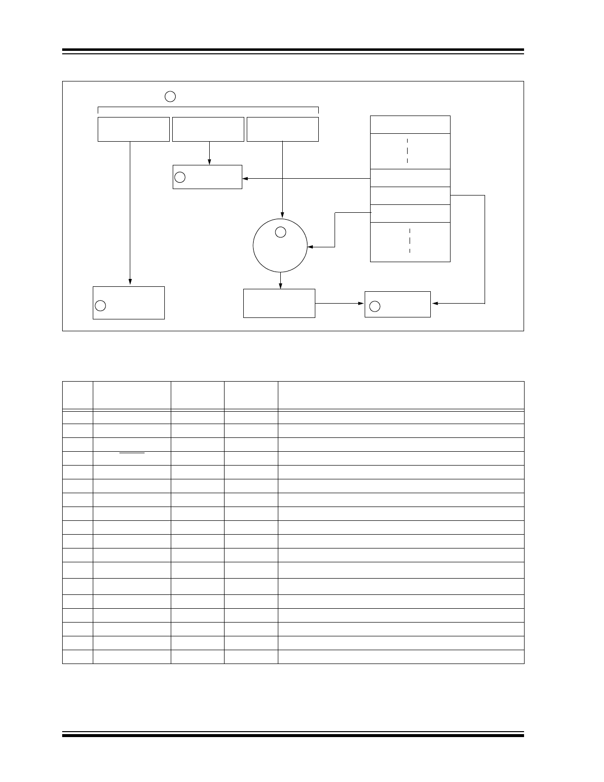
In normal operation, each received message of valid
format is evaluated. The serial number is used to deter-
mine if it is from a learned transmitter. If from a learned
transmitter, the message is decrypted and the synchro-
nization counter is verified. Finally, the button status is
checked to see what operation is requested. Figure 1-3
shows the relationship between some of the values
stored by the receiver and the values received from
the transmitter.
FIGURE 1-2:
BUILDING THE TRANSMITTED CODE WORD (ENCODER)
Transmitter
Manufacturer’s
Serial Number
Code
Crypt
Key
Key
Generation
Algorithm
Serial Number
Crypt Key
Sync Counter
.
.
.
HCS512
Production
Programmer
EEPROM Array
Button Press
Information
EEPROM Array
32 Bits
Encrypted Data
Serial Number
Transmitted Information
Crypt Key
Sync Counter
Serial Number
K
EE
L
OQ
®
Encryption
Algorithm
HCS512
DS40151E-page 4
© 2011 Microchip Technology Inc.
FIGURE 1-3:
BASIC OPERATION OF RECEIVER (DECODER)
NOTE: Circled numbers indicate the order of execution.
2.0
PIN ASSIGNMENT
PIN
Decoder
Function
I/O
(1)
Buffer
Type
(1)
Description
1
LRNIN
I
TTL
Learn input - initiates learning, 10K pull-up required on input
2
LRNOUT
O
TTL
Learn output - indicates learning
3
NC
—
TTL
Do not connect
4
MCLR
I
ST
Master clear input
5
Ground
P
—
Ground connection
6
S0
O
TTL
Switch 0
7
S1
O
TTL
Switch 1
8
S2
O
TTL
Switch 2
9
S3
O
TTL
Switch 3
10
V
LOW
O
TTL
Battery low indication output
11
SLEEP
I
TTL
Connect to RFIN to allow wake-up from SLEEP
12
CLK
I/O
TTL/ST
(2)
Clock in Programming mode and Synchronous mode
13
DATA
I/O
TTL/ST
(2)
Data in Programming mode and Synchronous mode
14
V
DD
P
—
Power connection
15
OSC
OUT
(1MH
Z
)
O
TTL
Oscillator out (test point)
16
OSC
IN
(4MHz)
I
ST
Oscillator in – recommended values 4.7 k
Ω and 22 pF
17
NC
—
—
18
RFIN
I
TTL
RF input from receiver
Note 1: P = power, I = in, O = out, and ST = Schmitt Trigger input.
2: Pin 12 and Pin 13 have a dual purpose. After RESET, these pins are used to determine if Programming
mode is selected in which case they are the clock and data lines. In normal operation, they are the clock
and data lines of the synchronous data output stream.
Button Press
Information
EEPROM Array
Manufacturer Code
32 Bits of
Encrypted Data
Serial Number
Received Information
Decrypted
Synchronization
Counter
Check for
Match
Sync Counter
Serial Number
K
EE
L
OQ®
Decryption
Algorithm
1
3
4
Check for
Match
2
Perform Function
Indicated by
button press
5
Crypt Key
© 2011 Microchip Technology Inc.
DS40151E-page 5
HCS512
3.0
DESCRIPTION OF FUNCTIONS
3.1
Parallel Interface
The HCS512 activates the S3, S2, S1 & S0 outputs
when a new valid code is received. The outputs will be
activated for approximately 500 ms. If a repeated code
is received during this time, the output extends for
approximately 500 ms.
3.2
Serial Interface
The decoder has a PWM/Synchronous interface con-
nection to microcontrollers with limited I/O. An output
data stream is generated when a valid transmission is
received. The data stream consists of one START bit,
four function bits, one bit for battery status, one bit to
indicate a repeated transmission, two status bits, and
one STOP bit. (Table 3-1). The DATA and CLK lines are
used to send a synchronous event message.
A special status message is transmitted on the second
pass of learn. This allows the controlling microcon-
troller to determine if the learn was successful (Result
= 1) and if a previous transmitter was overwritten
(Overwrite = 1). The status message is shown in
Figure 3-2.
Table 3-1 show the values for TX1:0 and the number of
transmitters learned.
TABLE 3-1:
STATUS BITS
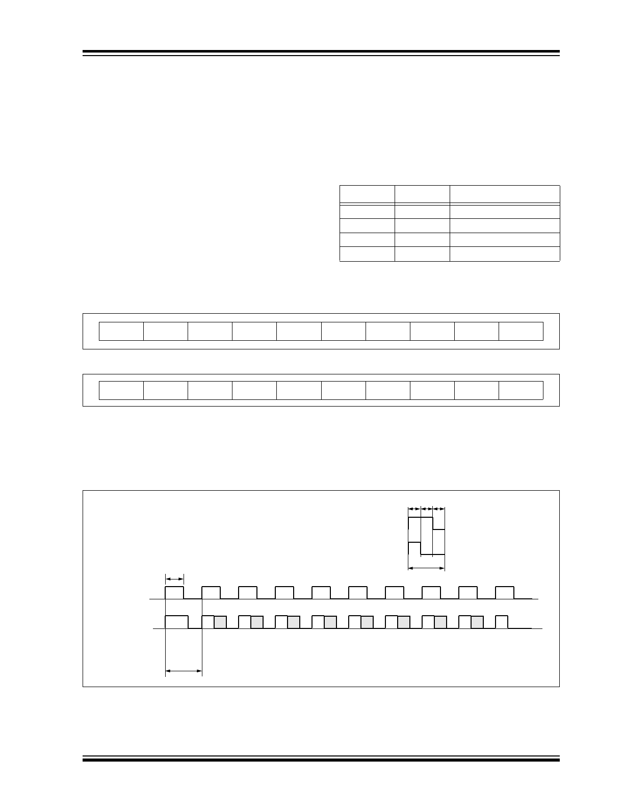
FIGURE 3-1:
DATA OUTPUT FORMAT
FIGURE 3-2:
STATUS MESSAGE FORMAT
A 1-wire PWM or 2-wire synchronous interface can be used.
In 1-wire mode, the data is transmitted as a PWM signal with a basic pulse width of 400
μs.
In 2-wire mode, Synchronous mode PWM bits start on the rising edge of the clock, and the bits must be sampled on the
falling edge. The START bit is a ‘1’ and the STOP bit is ‘0’.
FIGURE 3-2:
PWM OUTPUT FORMAT
(1)
Note:
The Decoder output PWM format logic (“1” / “0”) is reversed with respect of the Encoder modulation format.
TX1
TX0
Number of Transmitters
0
0
One
0
1
Two
1
0
Three
1
1
Four
START
S3
S2
S1
S0
V
LOW
TX1
TX0
STOP
REPEAT
START
0
0
0
0
RESULT
TX1
TX0
STOP
OVRWR
S3
START
S2
S1
S0
V
LOW
RPT
Reserved Reserved STOP
1200
μs
CLK
DATA
LOGIC “1”
LOGIC “0”
600
μs
1200
μs
1/31/3 1/3
HCS512
DS40151E-page 6
© 2011 Microchip Technology Inc.
4.0
DECODER OPERATION
4.1
Learning a Transmitter to a
Receiver
Either the serial number-based learning method or the
seed-based learning method can be selected. The
learning method is selected in the configuration byte. In
order for a transmitter to be used with a decoder, the
transmitter must first be ‘learned’. When a transmitter is
learned to a decoder, the decoder stores the crypt key,
a check value of the serial number and current syn-
chronization value in EEPROM. The decoder must
keep track of these values for every transmitter that is
learned. The maximum number of transmitters that can
be learned is four. The decoder must also contain the
Manufacturer’s Code in order to learn a transmitter.
The Manufacturer’s Code will typically be the same for
all decoders in a system.
The HCS512 has four memory slots. After an “erase all”
procedure, all the memory slots will be cleared. Erase
all is activated by taking LRNIN low for approximately
10 seconds. When a new transmitter is learned, the
decoder searches for an empty memory slot and stores
the transmitter’s information in that memory slot. When
all memory slots are full, the decoder randomly over-
writes existing transmitters.
4.1.1
LEARNING PROCEDURE
Learning is activated by taking the
LRNIN
input low for
longer than 64 ms. This input requires an external pull-
up resistor.
To learn a new transmitter to the HCS512 decoder, the
following sequence is required:
1.
Enter Learning mode by pulling LRNIN low for
longer than 64 ms. The LRNOUT output will go
high.
2.
Activate the transmitter until the LRNOUT out-
put goes low indicating reception of a valid code
(hopping message).
3.
Activate the transmitter a second time until the
LRNOUT toggles for 4 seconds (in Secure
Learning mode, the seed transmission must be
transmitted during the second stage of learn by
activating the appropriate buttons on the trans-
mitter).
If LRNIN is taken low momentarily during the
learn status indication, the indication will be ter-
minated. Once a successful learning sequence
is detected, the indication can be terminated
allowing quick learning in a manufacturing
setup.
4.
The transmitter is now learned into the decoder.
5.
Repeat steps 1-4 to learn up to four transmitters.
6.
Learning will be terminated if two non-sequential
codes were received or if two acceptable codes
were not decoded within 30 seconds.
The following checks are performed on the decoder to
determine if the transmission is valid during learn:
• The first code word is checked for bit integrity.
• The second code word is checked for bit integrity.
• The hopping code is decrypted.
• If all the checks pass, the serial number and syn-
chronization counters are stored in EEPROM
memory.
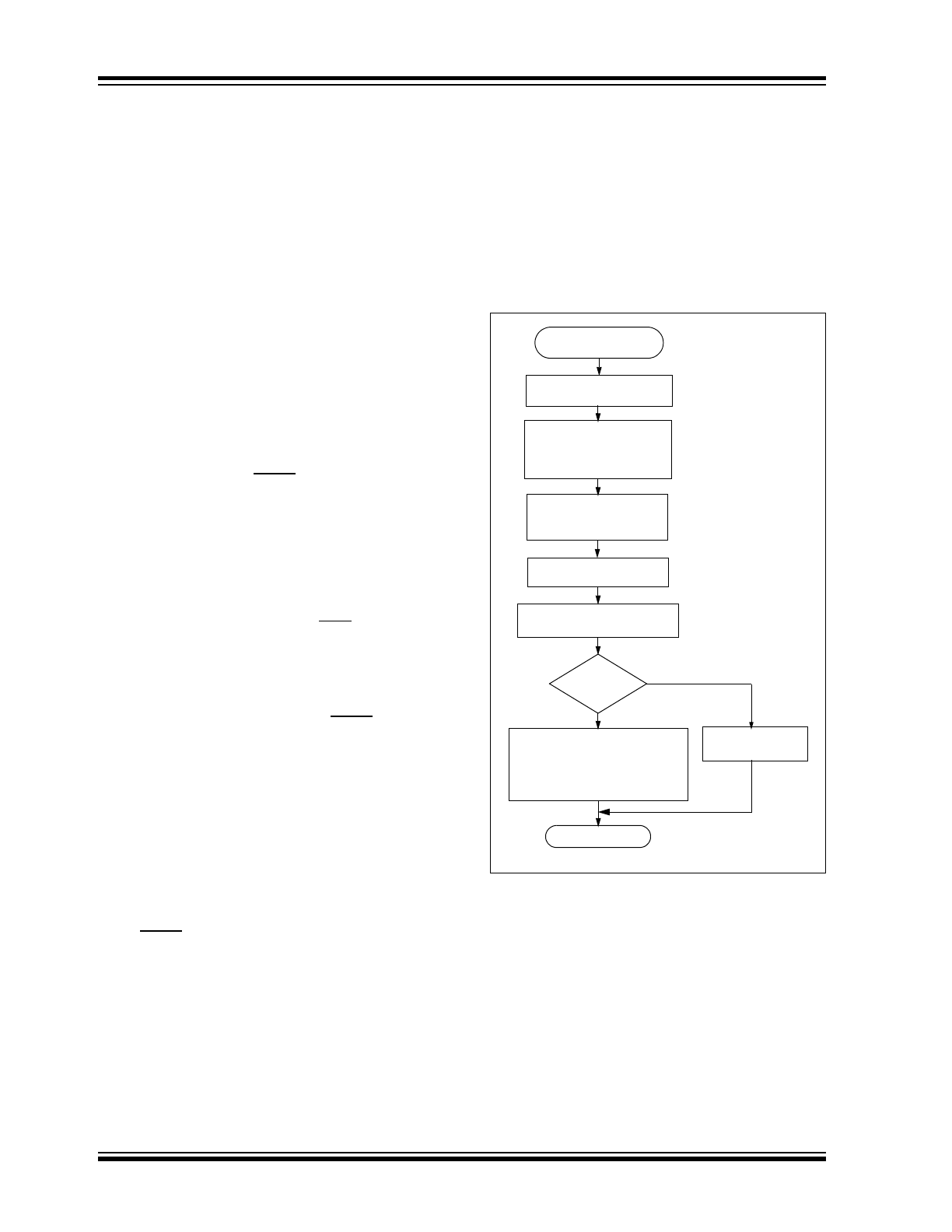
Figure 4-1 shows a flow chart of the learn sequence.
FIGURE 4-1:
LEARN SEQUENCE
Enter Learn
Mode
Wait for Reception
of Second
Compare Discrimination
Value with Serial Number
Use Generated Key
to Decrypt
Equal
Serial number check value
Synchronization counter
?
Exit
Learn successful. Store:
Learn
Unsuccessful
No
Yes
Wait for Reception
of a Valid Code
Non-Repeated
Valid Code
Generate Key
from Serial Number
or Seed Value
crypt key
© 2011 Microchip Technology Inc.
DS40151E-page 7
HCS512
4.2
Validation of Codes
The decoder waits for a transmission and checks the
serial number to determine if the transmitter has been
learned. If learned, the decoder decrypts the encrypted
portion of the transmission using the crypt key. It uses
the discrimination bits to determine if the decryption
was valid. If everything up to this point is valid, the
synchronization value is evaluated.
4.3
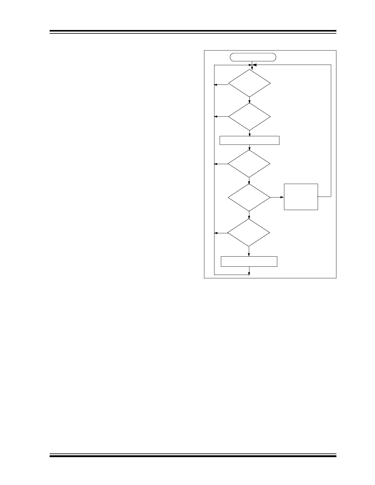
Validation Steps
Validation consists of the following steps:
• Search EEPROM to find the Serial Number
Check Value Match
• Decrypt the Hopping Code
• Compare the 10 bits of discrimination value with
the lower 10 bits of serial number
• Check if the synchronization counter falls within
the first synchronization window.
• Check if the synchronization counter falls within
the second synchronization window.
• If a valid transmission is found, update the syn-
chronization counter, else use the next transmitter
block and repeat the tests.
FIGURE 4-2:
DECODER OPERATION
?
Transmission
Received
Does
Ser # Check Val
Match
?
Decrypt Transmission
Is
Decryption
Valid
?
Is
Counter
Within 16
?
Is
Counter
Within 32K
?
Update
Counter
Execute
Command
Save Counter
in Temp Location
Start
No
No
No
No
Yes
Yes
Yes
Yes
Yes
No
and
HCS512
DS40151E-page 8
© 2011 Microchip Technology Inc.
4.4
Synchronization with Decoder
(Evaluating the Counter)
The K
EE
L
OQ
technology patent scope includes a
sophisticated synchronization technique that does not
require the calculation and storage of future codes. The
technique securely blocks invalid transmissions while
providing transparent resynchronization to transmitters
inadvertently activated away from the receiver.
Figure 4-3 shows a 3-partition, rotating synchronization
window. The size of each window is optional but the
technique is fundamental. Each time a transmission is
authenticated, the intended function is executed and
the transmission's synchronization counter value is
stored in EEPROM. From the currently stored counter
value there is an initial "Single Operation" forward win-
dow of 16 codes. If the difference between a received
synchronization counter and the last stored counter is
within 16, the intended function will be executed on the
single button press and the new synchronization coun-
ter will be stored. Storing the new synchronization
counter value effectively rotates the entire synchroniza-
tion window.
A "Double Operation" (resynchronization) window fur-
ther exists from the Single Operation window up to 32K
codes forward of the currently stored counter value. It
is referred to as "Double Operation" because a trans-
mission with synchronization counter value in this win-
dow will require an additional, sequential counter
transmission prior to executing the intended function.
Upon receiving the sequential transmission the
decoder executes the intended function and stores the
synchronization counter value. This resynchronization
occurs transparently to the user as it is human nature
to press the button a second time if the first was unsuc-
cessful.
The third window is a "Blocked Window" ranging from
the double operation window to the currently stored
synchronization counter value. Any transmission with
synchronization counter value within this window will
be ignored. This window excludes previously used,
perhaps code-grabbed transmissions from accessing
the system.
FIGURE 4-3:
SYNCHRONIZATION WINDOW
4.5
SLEEP Mode
The SLEEP mode of the HCS512 is used to reduce
current consumption when no RF input signal is pres-
ent. SLEEP mode will only be effective in systems
where the RF receiver is relatively quiet when no signal
is present. During SLEEP, the clock stops, thereby sig-
nificantly reducing the operating current. SLEEP mode
is enabled by the SLEEP bit in the configuration byte.
The HCS512 will enter SLEEP mode when:
• The RF line is low
• After a function output is switched off
• Learn mode is terminated (time-out reached)
The device will not enter SLEEP mode when:
• A function output is active
• Learn sequence active
• Device is in Programming mode
The device will wake-up from SLEEP when:
• The SLEEP input pin changes state
• The CLOCK line changes state
Note:
The synchronization method described in
this section is only a typical implementation
and because it is usually implemented in
firmware, it can be altered to fit the needs
of a particular system.
Blocked
Entire Window
rotates to eliminate
use of previously
used codes
Single Operation
Window
Window
(32K Codes)
(16 Codes)
Double Operation
(resynchronization)
Window
(32K Codes)
Stored
Synchronization
Counter Value
Note:
During SLEEP mode the CLK line will
change from an output line to an input line
that can be used to wake-up the device.
Connect CLK to
LRNIN
via a 100K resistor
to reliably enter the Learn mode whenever
SLEEP mode is active.
© 2011 Microchip Technology Inc.
DS40151E-page 9
HCS512
5.0
INTEGRATING THE HCS512
INTO A SYSTEM
The HCS512 can act as a stand-alone decoder or be
interfaced to a microcontroller. Typical stand-alone
applications include garage door openers and elec-
tronic door locks. In stand-alone applications, the
HCS512 will handle learning, reception, decryption,
and validation of the received code; and generate the
appropriate output. For a garage door opener, the
HCS512 input will be connected to an RF receiver, and
the output, to a relay driver to connect a motor control-
ler.
Typical systems where the HCS512 will be connected
to a microcontroller include vehicle and home security
systems. The HCS512 input will be connected to an RF
receiver and the function outputs to the microcontroller.
The HCS512 will handle all the decoding functions and
the microcontroller, all the system functions. The Serial
Output mode with a 1- or 2-wire interface can be used
if the microcontroller is I/O limited.
6.0
DECODER PROGRAMMING
The PG306001 production programmer will allow easy
setup and programming of the configuration byte and
the manufacturer’s code.
6.1
Configuration Byte
The configuration byte is used to set system configura-
tion for the decoder. The LRN bits determine which
algorithm (Decrypt or XOR) is used for the key genera-
tion. SC_LRN determines whether normal learn (key
derived from serial number) or secure learn (key
derived from seed value) is used.
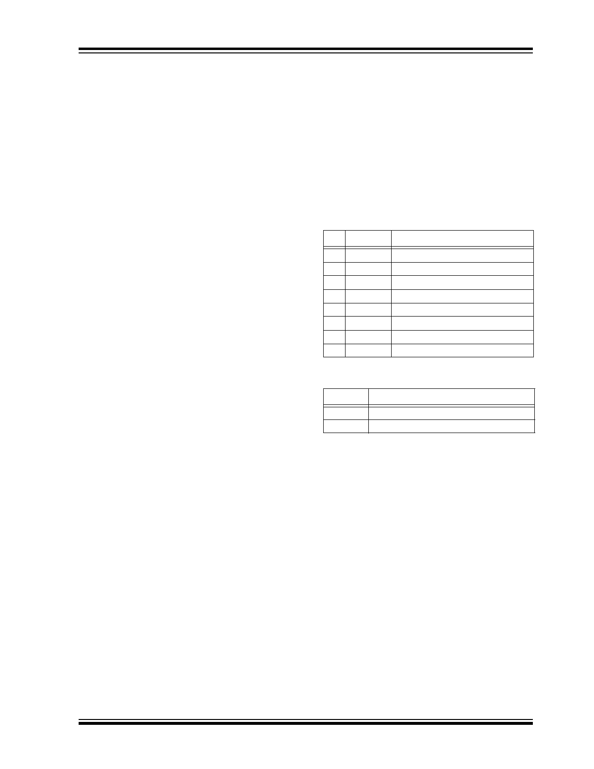
TABLE 6-1:
CONFIGURATION BYTE
TABLE 6-2:
LEARN METHOD LRN0, LRN1
DEFINITIONS
Bit
Name
Description
0
LRN0
Learn algorithm select
1
LRN1
Not used
2
SC_LRN Secure Learn enable (1 = enabled)
3
SLEEP
SLEEP enable (1 = enabled)
4
RES1
Not used
5
RES2
Not used
6
RES3
Not used
7
RES4
Not used
LRN0
Description
0
Decrypt algorithm
1
XOR algorithm
HCS512
DS40151E-page 10
© 2011 Microchip Technology Inc.
6.2
Programming the Manufacturer’s
Code
The manufacturer’s code must be programmed into
EEPROM memory through the synchronous program-
ming interface using the DATA and CLK lines. Provision
must be made for connections to these pins if the
decoder is going to be programmed in circuit.
Programming mode is activated if the CLK is low for at
least 1 ms and then goes high within 64 ms after power-
up, stays high for longer than 8 ms but not longer than
128 ms. After entering Programming mode the 64-bit
manufacturer’s code, 8-bit configuration byte, and 8-bit
checksum is sent to the device using the synchronous
interface. After receiving the 80-bit message the check-
sum is verified and the information is written to
EEPROM. If the programming operation was success-
ful, the HCS512 will respond with an Acknowledge
pulse.
After programming the manufacturer’s code, the
HCS512 decoder will automatically activate an
Erase All function, removing all transmitters from the
system.
6.3
Download Format
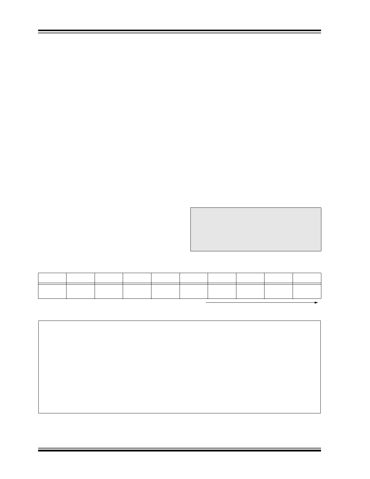
The manufacturer’s code and configuration byte must
be downloaded Least Significant Byte, Least Signifi-
cant bit first as shown in Table 6-3.
6.4
Checksum
The checksum is used by the HCS512 to check that the
data downloaded was correctly received before pro-
gramming the data. The checksum is calculated so that
the 10 bytes added together (discarding the overflow
bits) is zero. The checksum can be calculated by add-
ing the first 9 bytes of data together and subtracting the
result from zero. Throughout the calculation the over-
flow is discarded.
Given a manufacturer’s code of 01234567-
89ABCDEF
16
and a Configuration Word of 1
16
, the
checksum is calculated as shown in Figure 6-1. The
checksum is 3F
16
.
6.5
Test Transmitter
The HCS512 decoder will automatically add a test
transmitter each time an Erase All Function is done. A
test transmitter is defined as a transmitter with a serial
number of zero. After an Erase All, the test transmitter
will always work without learning and will not check the
synchronization counter of the transmitter. Learning of
any new transmitters will erase the test transmitter.
TABLE 6-3:
DOWNLOAD DATA
FIGURE 6-1:
CHECKSUM CALCULATION
Note 1: A transmitter with a serial number of zero
cannot be learned. Learn will fail after the
first transmission.
2: Always learn at least one transmitter after
an Erase All sequence. This ensures that
the test transmitter is erased.
Byte 9
Byte 8
Byte 7
Byte 6
Byte 5
Byte 4
Byte 3
Byte 2
Byte 1
Byte 0
Check-
sum
Config
Man
Key_7
Man
Key_6
Man
Key_5
Man
Key_4
Man
Key_3
Man
Key_2
Man
Key_1
Man
Key_0
Byte 0, right-most bit downloaded first.
01
16
+ 23
16
= 24
6
24
16
+ 45
16
= 69
16
69
16
+ 67
16
= D0
16
D0
16
+ 89
16
= 159
16
59
16
+ AB
16
= 104
16
(Carry is discarded)
04
16
+ CD
16
= D1
16
(Carry is discarded)
D1
16
+ EF
16
= 1C0
16
C0
16
+ 1
16
= C1
16
(Carry is discarded)
(FF
16
- C1
16
) + 1
16
= 3F
16