
© 2011 Microchip Technology Inc.
DS41099D-page 1
FEATURES
Security
• Programmable 64-bit encoder crypt key
• Two 64-bit IFF keys
• Keys are read protected
• 32-bit bi-directional challenge and response using
one of two possible keys
• 69-bit transmission length
• 32-bit hopping code,
• 37-bit nonencrypted portion
• Programmable 28/32-bit serial number
• 60-bit, read protected seed for secure learning
• Two IFF encryption algorithms
• Delayed counter increment mechanism
• Asynchronous transponder communication
• Transmissions include button Queuing
information
Operating
• 2.0V to 6.3V operation
• Three switch inputs: S2, S1, S0 – seven functions
• Battery-less bi-directional transponder capability
• Selectable baud rate and code word blanking
• Automatic code word completion
• Battery low detector
• PWM or Manchester data encoding
• Combined transmitter, transponder operation
• Anticollision of multiple transponders
• Passive proximity activation
• Device protected against reverse battery
• Intelligent damping for high Q LC-circuits
• 100 mV
PP
sensitive LC input
Typical Applications
• Automotive remote entry systems
• Automotive alarm systems
• Automotive immobilizers
• Gate and garage openers
• Electronic door locks (Home/Office/Hotel)
• Burglar alarm systems
• Proximity access control
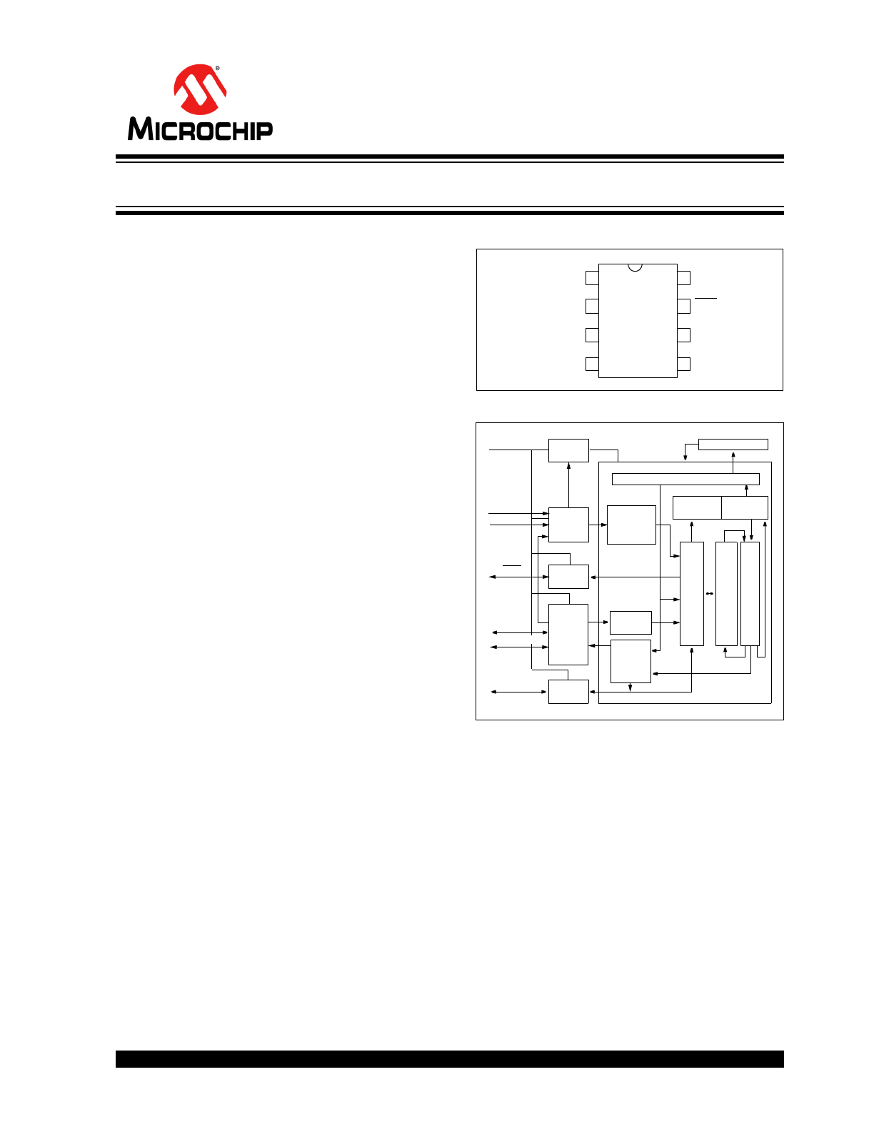
PACKAGE TYPES
BLOCK DIAGRAM
Other
• Simple programming interface
• On-chip tunable RC oscillator, ± 10%
• On-chip EEPROM
• 64-bit user EEPROM in Transponder mode
• Battery-low LED indication
• Serialized Quick Turn Programming (SQTP
SM
)
• 8-pin PDIP/SOIC
• RF Enable output
• ASK and FSK PLL interface option
• Built in LC input amplifier
HCS4
12
S0
S1
S2/RFEN/LC1
LC0
V
DD
LED
DATA
GND
1
8
2
3
4
7
6
5
PDIP, SOIC
Oscillator
Configuration Register
Power
Control
Wake-up
Logic
Address
Decoding EEPROM
Debounce
Control
and
Queuer
LED
Control
DATA
Driver
PPM
Detector
DATA
PPM
Manch.
Encoder
T
ran
sp
on
de
r
Ci
rc
ui
tr
y
C
o
nt
ro
l Lo
gi
c
an
d Cou
nt
e
rs
E
ncr
yp
tio
n
/Inc
re
m
e
nt
Lo
gi
c
R
egister
V
DD
S0
S1
LED
LC0
DATA
RFEN/S2/LC1
HCS412
K
EE
L
OQ®
Code Hopping Encoder and Transponder

HCS412
DS41099D-page 2
© 2011 Microchip Technology Inc.
GENERAL DESCRIPTION
The HCS412 combines patented K
EE
L
OQ®
code hop-
ping technology with bi-directional transponder chal-
lenge-and-response security into a single chip solution
for logical and physical access control.
When used as a code hopping encoder, the HCS412 is
ideally suited to keyless entry systems; vehicle and
garage door access in particular. The same HCS412
can also be used as a secure bi-directional transponder
for contactless token verification. These capabilities
make the HCS412 ideal for combined secure access
control and identification applications, dramatically
reducing the cost of hybrid transmitter/transponder
solutions.
1.0
SYSTEM OVERVIEW
Key Terms
The following is a list of key terms used throughout this
data sheet. For additional information on terminology,
please refer to the K
EE
L
OQ
introductory Technical Brief
(TB003).
• RKE - Remote Keyless Entry.
• PKE - Passive Keyless Entry.
• Button Status - Indicates what transponder but-
ton input(s) activated the transmission. Encom-
passes the 4 button status bits LC0, S2, S1 and
S0 (Figure 3-2).
• Code Hopping - A method by which a code,
viewed externally to the system, appears to
change unpredictably each time it is transmitted
(Section 1.1.3).
• Code word - A block of data that is repeatedly
transmitted upon button activation (Section 3.2).
• Transmission - A data stream consisting of
repeating code words.
• Crypt key - A unique and secret 64-bit number
used to encrypt and decrypt data. In a symmetri-
cal block cipher such as the K
EE
L
OQ
algorithm,
the encryption and decryption keys are equal and
will therefore be referred to generally as the crypt
key.
• Encoder - A device that generates and encodes
data.
• Encryption Algorithm - A recipe whereby data is
scrambled using a crypt key. The data can only be
interpreted by the respective decryption algorithm
using the same crypt key.
• Decoder - A device that decodes data received
from an encoder.
• Transponder Reader (Reader, for short) - A
device that authenticates a token using bi-direc-
tional communication.
• Decryption algorithm - A recipe whereby data
scrambled by an encryption algorithm can be
unscrambled using the same crypt key.
• Learn – Learning involves the receiver calculating
the transmitter’s appropriate crypt key, decrypting
the received hopping code and storing the serial
number, synchronization counter value and crypt
key in EEPROM (Section 6.1). The K
EE
L
OQ
prod-
uct family facilitates several learning strategies to
be implemented on the decoder. The following are
examples of what can be done.
- Simple Learning
The receiver uses a fixed crypt key, common
to all components of all systems by the same
manufacturer, to decrypt the received code
word’s encrypted portion.
- Normal Learning
The receiver uses information transmitted
during normal operation to derive the crypt
key and decrypt the received code word’s
encrypted portion.
- Secure Learn
The transmitter is activated through a special
button combination to transmit a stored 60-bit
seed value used to generate the transmitter’s
crypt key. The receiver uses this seed value
to derive the same crypt key and decrypt the
received code word’s encrypted portion.
• Manufacturer’s code - A unique and secret 64-
bit number used to generate unique encoder crypt
keys. Each encoder is programmed with a crypt
key that is a function of the manufacturer’s code.
Each decoder is programmed with the manufac-
turer code itself.
• Anticollision - A scheme whereby transponders
in the same field can be addressed individually
preventing simultaneous response to a command
(Section 4.3.1).
• IFF - Identify Friend or Foe (Section 1.2).
• Proximity Activation - A method whereby an
encoder automatically initiates a transmission in
response to detecting an inductive field
(Section 4.4.1).
• Transport code - An access code, ‘password’
known only by the manufacturer, allowing pro-
gram access to certain secure device memory
areas (Section 4.3.3).
• AGC - Automatic Gain Control.
© 2011 Microchip Technology Inc.
DS41099D-page 3
HCS412
1.1
Encoder Overview
The HCS412 code hopping transcoder is designed
specifically for passive entry systems; primarily vehicle
access. The transcoder portion of a passive entry sys-
tem is integrated into a transmitter, carried by the user
and operated to gain access to a vehicle or restricted
area. The HCS412 is meant to be a cost-effective yet
secure solution to such systems, requiring very few
external components (Figure 2-6).
1.1.1
LOW-END SYSTEM SECURITY RISKS
Most low-end keyless entry transmitters are given a
fixed identification code that is transmitted every time a
button is pushed. The number of unique identification
codes in a low-end system is usually a relatively small
number. These shortcomings provide an opportunity
for a sophisticated thief to create a device that ‘grabs’
a transmission and retransmits it later, or a device that
quickly ‘scans’ all possible identification codes until the
correct one is found.
1.1.2
HCS412 SECURITY
The HCS412, on the other hand, employs the K
EE
L
OQ
code hopping technology coupled with a transmission
length of 69 bits to virtually eliminate the use of code
‘grabbing’ or code ‘scanning’. The high security level of
the HCS412 is based on the patented K
EE
L
OQ
technol-
ogy. A block cipher based on a block length of 32 bits
and a key length of 64 bits is used. The algorithm
obscures the information in such a way that even if the
transmission information (before coding) differs by only
one bit from that of the previous transmission, statisti-
cally greater than 50 percent of the next transmission’s
encrypted bits will change.
1.1.3
HCS412 HOPPING CODE
The 16-bit synchronization counter is the basis behind
the transmitted code word changing for each transmis-
sion; it increments each time a button is pressed.
Once the device detects a button press, it reads the
button inputs and updates the synchronization counter.
The synchronization counter and crypt key are input to
the encryption algorithm and the output is 32 bits of
encrypted information. This encrypted data will change
with every button press, its value appearing externally
to ‘randomly hop around’, hence it is referred to as the
hopping portion of the code word. The 32-bit hopping
code is combined with the button information and serial
number to form the code word transmitted to the
receiver. The code word format is explained in greater
detail in Section 3.2.
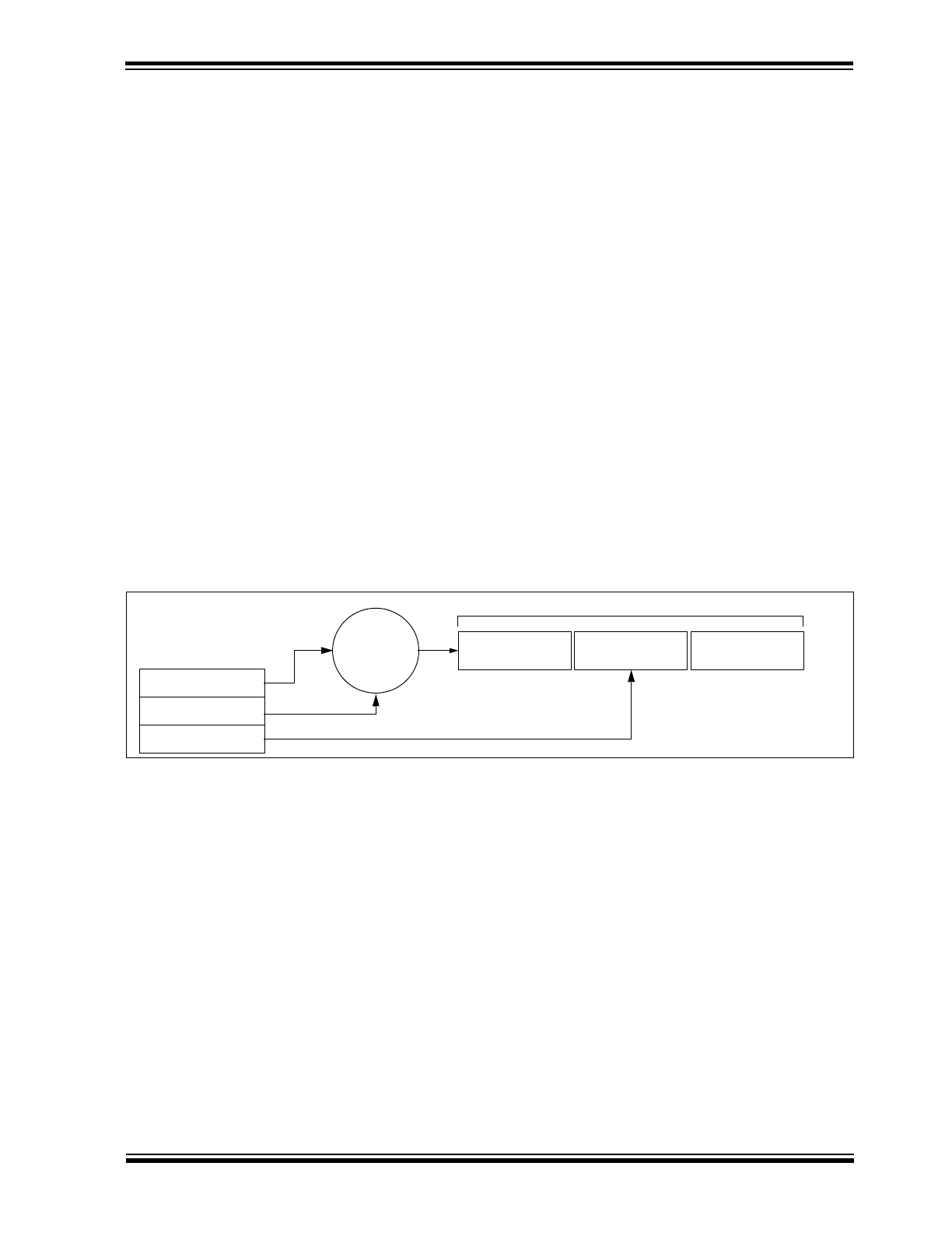
FIGURE 1-1:
BUILDING THE TRANSMITTED CODE WORD (ENCODER)
1.2
Identify Friend or Foe (IFF) Overview
Validation of a token first involves an authentication
device sending a random challenge to the token. The
token then replies with a calculated response that is a
function of the received challenge and the stored crypt
key. The authentication device, transponder reader,
performs the same calculation and compares it to the
token’s response. If they match, the token is identified
as valid and the transponder reader can take appropri-
ate action.
The HCS412’s 32-bit IFF response is generated using
one of two possible encryption algorithms and one of
two possible crypt keys; four combinations total. The
authenticating device precedes the challenge with a
five bit command word dictating which algorithm and
key to use in calculating the response.
The bi-directional communication path required for IFF
is typically inductive for short range (<10cm) transpon-
der applications and an inductive challenge, RF
response for longer range (~1.5m) passive entry appli-
cations.
Button Press
Information
EEPROM Array
32 Bits of
Encrypted Data
Serial Number
Transmitted Information
Crypt Key
Sync Counter
Serial Number
K
EE
L
OQ®
Encryption
Algorithm
HCS412
DS41099D-page 4
© 2011 Microchip Technology Inc.
2.0
DEVICE DESCRIPTION
2.1
Pinout Description
The HCS412’s footprint is identical to other encoders in
the K
EE
L
OQ
family, except for the two pins reserved for
low frequency communication.
TABLE 2-1:
PINOUT SUMMARY
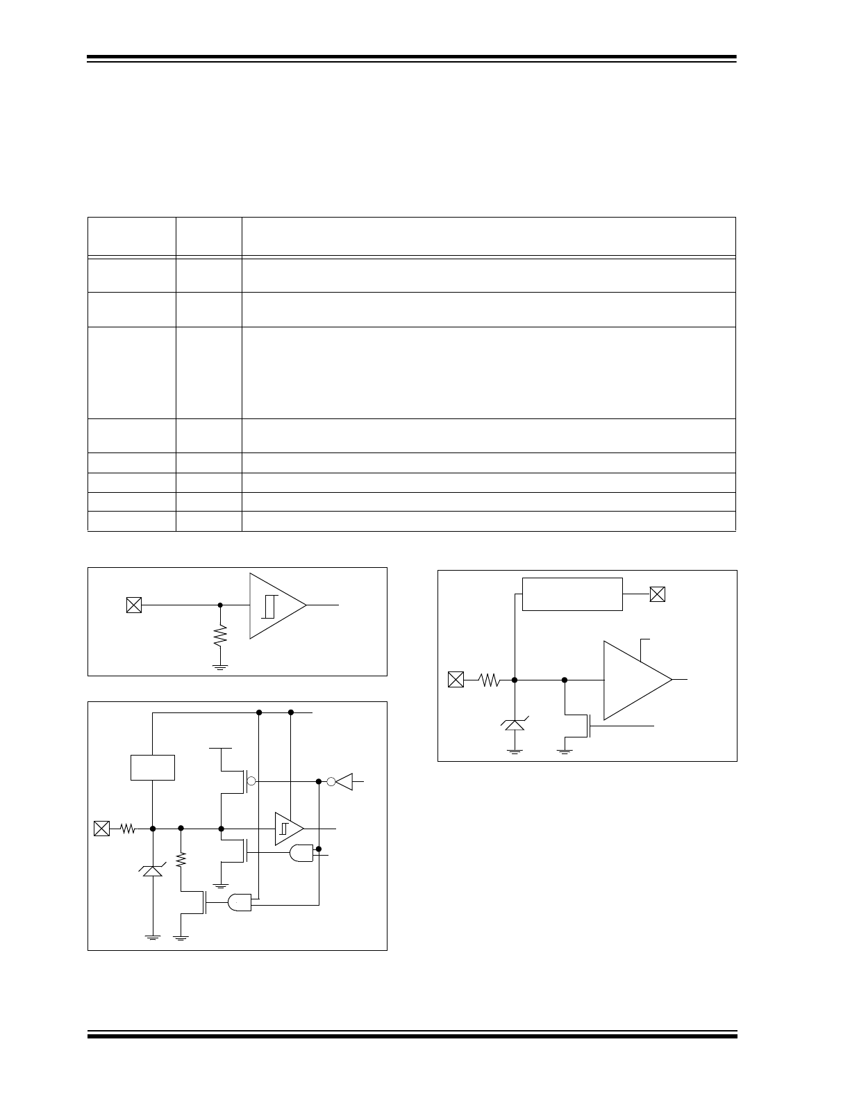
FIGURE 2-1:
S0/S1 PIN DIAGRAM
FIGURE 2-2:
S2/RFEN/LC1 PIN DIAGRAM
FIGURE 2-3:
LC0 PIN DIAGRAM
Pin
Name
Pin
Number
Description
S0
1
Button input pin with Schmitt Trigger detector and internal 60 k
Ω (nominal) pull-down
resistor (Figure 2-1).
S1
2
Button input pin with Schmitt Trigger detector and internal 60 k
Ω (nominal) pull-down
resistor (Figure 2-1).
S2/RFEN/LC1
3
Multi-purpose input / output pin (Figure 2-2).
• Button input pin with Schmitt Trigger detector and internal pull-down resistor.
• RFEN output driver.
• LC1 low frequency (LF) antenna output driver for inductive responses and LC bias.
• Programming clock signal input.
LC0
4
Low frequency (LF) antenna input with automatic gain control for inductive reception and
low frequency output driver for inductive responses (Figure 2-3).
GND
5
Ground reference.
DATA
6
Transmission data output driver. Programming input / output data signal (Figure 2-4).
LED
7
LED output driver (Figure 2-5).
V
DD
8
Positive supply voltage.
60 k
Ω
SWITCH
IN
S0
S1
>
10V
100
Ω
VBIAS
V
DD
SWITCH 2
INPUT
S2LC OPTION
LC
OUTPUT
RFEN
OUT
>
<
>
RECTIFIER AND
REGULATOR
V
DD
10V
100
Ω
LC
INPUT
LC
OUTPUT
S2LC OPTION
AMP
DET
AND
>
<
LC0
© 2011 Microchip Technology Inc.
DS41099D-page 5
HCS412
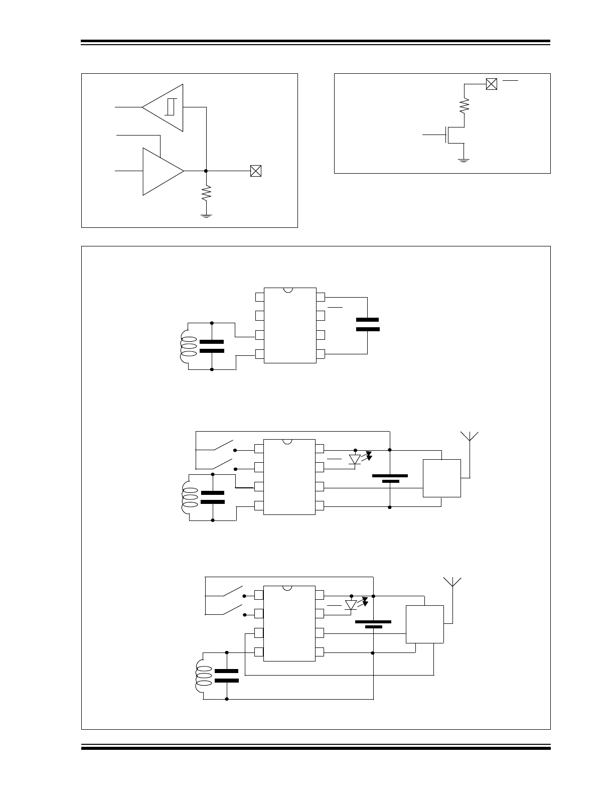
FIGURE 2-4:
DATA PIN DIAGRAM
FIGURE 2-5:
LED PIN DIAGRAM
FIGURE 2-6:
TYPICAL APPLICATION CIRCUITS
120 k
Ω
OE
DATA
DATA
IN
DATA
OUT
>
<
>
LED_ON
>
LED
R
HCS412
S0
S1
LC1
LC0
V
DD
LED
DATA
GND
1
8
2
3
4
7
6
5
HCS41
2
S0
S1
LC1
LC0
V
DD
LED
DATA
GND
1
8
2
3
4
7
6
5
RF
H
C
S412
S0
S1
RFEN
LC0
V
DD
LED
DATA
GND
1
8
2
3
4
7
6
5
RF
Battery-less Short Range Transponder
Long Range / Proximity Activated Transponder / Encoder
Short Range Transponder with RFEN Control / Long Range Encoder

HCS412
DS41099D-page 6
© 2011 Microchip Technology Inc.
2.2
Architecture Overview
2.2.1
WAKE-UP LOGIC AND POWER
DISTRIBUTION
The HCS412 automatically goes into a low-power
Standby mode once connected to the supply voltage.
Power is supplied to the minimum circuitry required to
detect a wake-up condition; button activation or LC sig-
nal detection.
The HCS412 will wake from Low-power mode when a
button input is pulled high or a signal is detected on the
LC0 LF antenna input pin. Waking involves powering
the main logic circuitry that controls device operation.
The button and transponder inputs are then sampled to
determine which input activated the device.
A button input activation places the device into Encoder
mode. A signal detected on the transponder input
places the device into Transponder mode. Encoder
mode has priority over Transponder mode so a signal
on the transponder input would be ignored if it occurred
simultaneously to a button activation; ignored until the
button input is released.
2.2.2
CONTROL LOGIC
A dedicated state machine, timer and a 32-bit shift reg-
ister perform the control, timing and data manipulation
in the HCS412. This includes the data encryption, data
output modulation and reading of and writing to the
onboard EEPROM.
2.2.3
EEPROM
The HCS412 contains nonvolatile EEPROM to store
configuration options, user data and the synchroniza-
tion counter.
The configuration options are programmed during pro-
duction and include the read protected security-related
information such as crypt keys, serial number and dis-
crimination value (Table 7-2).
The 64 bits (4x16-bit words) of user EEPROM are read/
write accessible through the low frequency communi-
cation path as well as in-circuit, wire programmable
during production.
The initial synchronization counter value is pro-
grammed during production. The counter is imple-
mented in Grey code and updated using bit writes to
minimize EEPROM writing over the life of the product.
The user need not worry about counter format conver-
sion as the transmitted counter value is in binary for-
mat.
Counter corruption is protected for by the use of a
semaphore word as well as by the internal circuitry
ensuring the EEPROM write voltage is at an accept-
able level prior to each write.
The EEPROM is programmed during production by
clocking (S2 pin) the data into the DATA pin
(Section 7.0). Certain EEPROM locations can also be
remotely read/written through the LF communication
path (Section 4.3).
2.2.4
CONFIGURATION REGISTER
The first activation after connecting power to the
HCS412, the device retrieves the configuration from
EEPROM storage and buffers the information in a con-
figuration register. The configuration register then dic-
tates various device operation options including the RC
oscillator tuning, the S2/RFEN/LC1 pin configuration,
low voltage trip point, modulation format,...
2.2.5
ONBOARD RC OSCILLATOR AND
OSCILLATOR TUNE VALUE (OSCT)
The HCS412 has an onboard RC oscillator. As the RC
oscillator is susceptible to variations in process param-
eters, temperature and operating voltage, oscillator
tuning is provided for more accurate timing character-
istics.
The 4-bit Oscillator Tune Value (OSCT) (Table 2-2)
allows tuning within ±4% of the optimal oscillator speed
at the voltage and temperature used when tuning the
device. A properly tuned oscillator is then accurate over
temperature and voltage variations to within ±10% of
the tuned value.
Oscillator speed is significantly affected by changes in
the device supply voltage. It is therefore best to tune
the HCS412 such that the variance in oscillator speed
be symmetrical about an operating mid-point
(Figure 2-7). ie...
• If the design is to run on a single lithium battery,
tune the oscillator while supplying the HCS412
with ~2.5V (middle of the 3V to 2V usable battery
life).
• If the design is to run on two lithium batteries, tune
the oscillator while supplying the HCS412 with
~4V (middle of 6V to 2V battery life).
• If the design is to run on 5V, tune the oscillator
while supplying the HCS412 with 5V.
Say the HCS412’s oscillator is tuned to be optimal at a
6V supply voltage but the device will operate on a sin-
gle lithium battery. The resulting oscillator variance
over temperature and voltage will not be ±4% but will
be more like -7% to -15%.
Programming using a supply voltage other than 5V
may not be practical. In these cases, adjust the oscilla-
tor tune value such that the device will run optimally at
the target voltage. (i.e., If programming using 5V a
device that will run at 3V, program the device to run
slow at 5V such that it will run optimally at 3V).

© 2011 Microchip Technology Inc.
DS41099D-page 7
HCS412
TABLE 2-2:
OSCILLATOR CALIBRATION
VALUE (OSCT)
FIGURE 2-7:
HCS412 NORMALIZED RF
TE
VERSUS TEMP
2.2.6
LOW VOLTAGE DETECTOR
The HCS412’s battery voltage detector detects when
the supply voltage drops below a predetermined value.
The value is selected by the Low Voltage Trip Point
Select (VLOWSEL) configuration option.
The low voltage detector result is included in encoder
transmissions (VLOW) allowing the receiver to indicate
when the transmitter battery is low (Figure 3-2).
The HCS412 indicates a low battery condition by
changing the LED operation (Figure 3-9).
FIGURE 2-8:
TYPICAL VOLTAGE TRIP
POINTS
TABLE 2-3:
VLOWSEL OPTIONS
TABLE 2-4:
VLOW STATUS BIT
2.2.7
THE S2/RFEN/LC1 PIN
The S2/RFEN/LC1 pin may be used as a button input,
RF enable output or as an interface to the LF antenna.
Select between LC1 antenna interface and S2/RFEN
functionality with the button/transponder select (S2LC)
configuration option (Table 2-2).
2.2.7.1
S2 BUTTON INPUT CONSIDERATIONS
The S2/RFEN/LC1 pin defaults to LF antenna output
LC1 when the HCS412 is first connected to the supply
voltage (i.e., battery replacement).
The configuration register controlling the pin’s function
is loaded on the first device activation after battery
replacement. A desired S2 input state is therefore
enabled only after the first activation of either S0, S1 or
LC0. The transponder bias circuitry switches off and
the internal pull-down resistor is enabled when the S2/
RFEN/LC1 pin reaches button input configuration.
There will be an extra delay the first activation after
connecting to the supply voltage while the HCS412
retrieves the configuration word and configures the
pins accordingly.
OSCT3:0
Description
0111b
Slowest Oscillator Setting (long T
E
)
+
:
0011b
0010b
0001b
:
Slower (longer T
E
)
:
0000b
Nominal Setting
1111b
1110b
1101b
:
Faster (shorter T
E
)
:
-
:
1000b
Fastest Oscillator Setting (short T
E
)
0.94
1.10
1.08
1.06
1.04
1.02
1.00
0.98
0.96
0.92
0.90
RF
TE
RF
TE
V
DD
LEGEND
= 2.0V
= 3.0V
= 6.0V
NORMALIZED
Temperature °C
-50 -40 -30 -20 -10 0 10 20 30 40 50 60 70 80 90
Note:
Values are for calibrated oscillator.
RF
TE
VLOWSEL
Nominal
Trip
Point
Description
0
2.2V
for 3V battery applications
1
4.4V
for 6V battery applications
VLOW
Description
0
V
DD
is above selected trip voltage
1
V
DD
is below selected trip voltage
V
LOW
Volts (V)
-40
0
50
85
2.0
1.6
1.8
2.2
2.4
2.6
Temp (°C)
V
LOW
sel = 0
4.4
4.0
4.2
3.8
4.6
4.8
5.0
V
LOW
sel = 1
2.8
Nominal V
LOW
trip point

HCS412
DS41099D-page 8
© 2011 Microchip Technology Inc.
2.2.7.2
TRANSPONDER INTERFACE
Connecting an LC resonant circuit between the LC0
and the LC1 pins creates the bi-directional low fre-
quency communication path with the HCS412.
The internal circuitry on the HCS412 provides the fol-
lowing functions:
• LF input amplifier and envelope detector to detect
and shape the incoming low frequency excitation
signal.
• 10V zener input protection from excessive
antenna voltage generated when proximate to
very strong magnetic fields.
• LF antenna clamping transistors for inductive
responses back to the transponder reader. The
antenna ends are shorted together, ‘clamped’,
dissipating the oscillatory energy. The reader
detects this as a momentary load on its excitation
antenna.
• Damping circuitry that improves communication
when using high-Q LC antenna circuits.
• Incoming LF energy rectification and regulation
for the supply voltage in battery-less or low bat-
tery transponder instances.
During normal transponder operation, the LC1 pin func-
tions to bias the LC0 AGC amplifier input. The amplifier
gain control sets the optimum level of amplification in
respect to the incoming signal strength. The signal then
passes through an envelope detector before interpreta-
tion in the logic circuit.
2.2.7.3
RF ENABLE OUTPUT
When the RF enable (RFEN) configuration option is
enabled, the RFEN signal output is coordinated with
the DATA output pin to provide typical ASK or FSK PLL
activation.
TABLE 2-1:
RFEN OPTION
TABLE 2-2:
S2/RFEN/LC1 CONFIGURATION OPTION
3.0
ENCODER OPERATION
3.1
Encoder Activation
3.1.1
BUTTON ACTIVATION
The main way to enter Encoder mode is when the
wake-up circuit detects a button input activation; button
input transition from GND to V
DD
. The HCS412 control
logic wakes and delays a switch debounce time prior to
sampling the button inputs. The button input states,
cumulatively called the button status, determine
whether the HCS412 transmits a code hopping or seed
transmission, Table 3-1.
Additional button activations added during a transmis-
sion will immediately RESET the HCS412, perhaps
leaving the current code word incomplete. The device
will start a new transmission which includes the
updated button code value.
Buttons removed during a transmission will have no
effect unless no buttons remain activated. If no button
activations remain, the minimum number of compete
code words will be completed (Section 3.4.1) and the
device will return to Standby mode.
3.1.2
PROXIMITY ACTIVATION
The other way to enter Encoder mode is if the S2/LC
option is configured for LC operation and the wake-up
circuit detects a signal on the LC0 LF antenna input pin.
This form of activation is called Proximity activation as
a code hopping transmission would be initiated when
the device was proximate to a LF field.
Refer to Section 4.4 for details on configuring the
HCS412 for Proximity Activation.
RFEN
Description
0
RF Enable output is disabled.
1
RF Enable output is enabled.
S2LC
Resulting S2/RFEN/LC1 Configuration
0
• LC1 low frequency antenna output driver for inductive responses and LC bias.
Note: LC0 low frequency antenna input is also enabled.
1
• S2 button input pin with Schmitt Trigger detector and internal pull-down resistor.
• RFEN output driver.
Note: LC0 and LC1 low frequency antenna interfaces are disabled and the transponder circuitry is
switched off to reduce standby current.
© 2011 Microchip Technology Inc.
DS41099D-page 9
HCS412
TABLE 3-1:
ENCODER MODE ACTIVATION
3.2
Transmitted Code Word
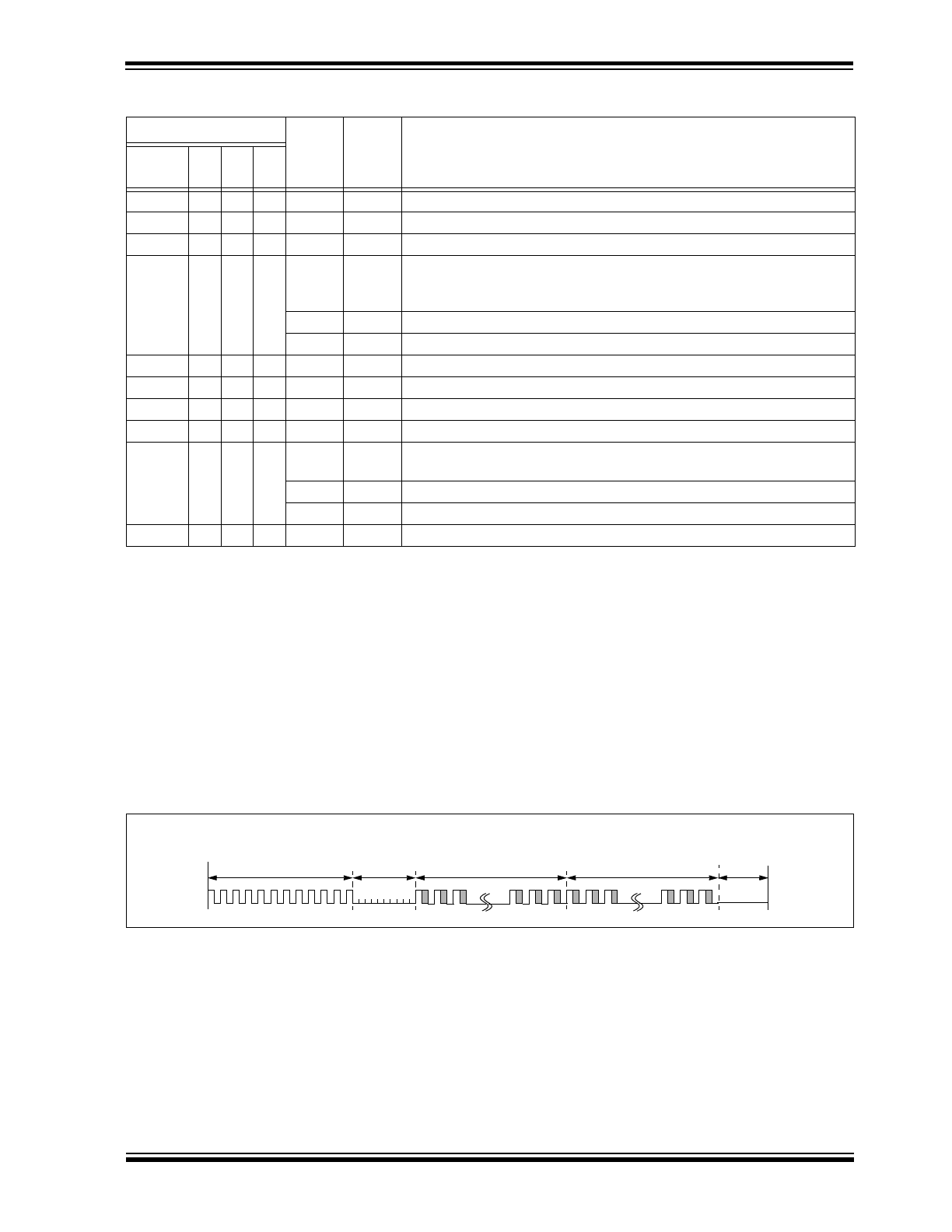
The HCS412 transmits a 69-bit code word in response
to a button or proximity activation (Figure 3-1). Each
code word contains a 50% duty cycle preamble,
header, 32 bits of encrypted data and 37 bits of fixed
code data followed by a guard period before another
code word can begin.
The 32 bits of Encrypted Data include 4 button bits, 2
counter overflow bits, 10 discrimination bits and the 16-
bit synchronization counter value (Figure 3-2).
The content of the 37 bits of Fixed Code Data varies
with the extended serial number (XSER) option
(Figure 3-2).
• If the extended serial number option is disabled
(XSER = 0), the 37 bits include 5 status bits, 4
button status bits and the 28-bit serial number.
• If the extended serial number option is enabled
(XSER = 1), the 37 bits include 5 status bits and
the 32-bit serial number.
FIGURE 3-1:
CODE WORD FORMAT
4-Bit Button Status
SEED TMPSD
Resulting Transmission
LC0
(Note 1)
S2 S1 S0
X
0
0
1
X
X
Code hopping transmission
X
0
1
0
X
X
Code hopping transmission
X
0
1
1
0
0
Code hopping transmission
0
1
Code hopping code words until time = T
DSD
, then seed code words.
SEED transmissions temporarily enabled until the 7lsb’s of the synchro-
nization counter wrap 7Fh to 00h. Then only code hopping code words.
1
0
Code hopping code words until time = T
DSD
, then seed code words.
1
1
Code hopping transmission (2 key IFF enabled)
X
1
0
1
X
X
Code hopping transmission
X
1
0
0
X
X
Code hopping transmission
X
1
1
0
X
X
Code hopping transmission
X
1
1
1
0
0
Code hopping transmission
0
1
Limited SEED transmissions - temporarily enabled until the 7lsb’s of the
synchronization counter wrap 7Fh to 00h.
1
0
SEED transmission
1
1
Code hopping transmission (2 key IFF enabled)
1
0
0
0
X
X
Proximity activated code hopping transmission.
Note 1: The transmitted button status will reflect the state of the LC0 input when the button inputs are sampled.
Preamble
Header
Encrypted Portion
of Transmission
Fixed Portion of
Transmission
Guard
Time
T
P
T
H
T
HOP
T
FIX
T
G
50% Duty Cycle
HCS412
DS41099D-page 10
© 2011 Microchip Technology Inc.
FIGURE 3-2:
CODE WORD ORGANIZATION
3.2.1
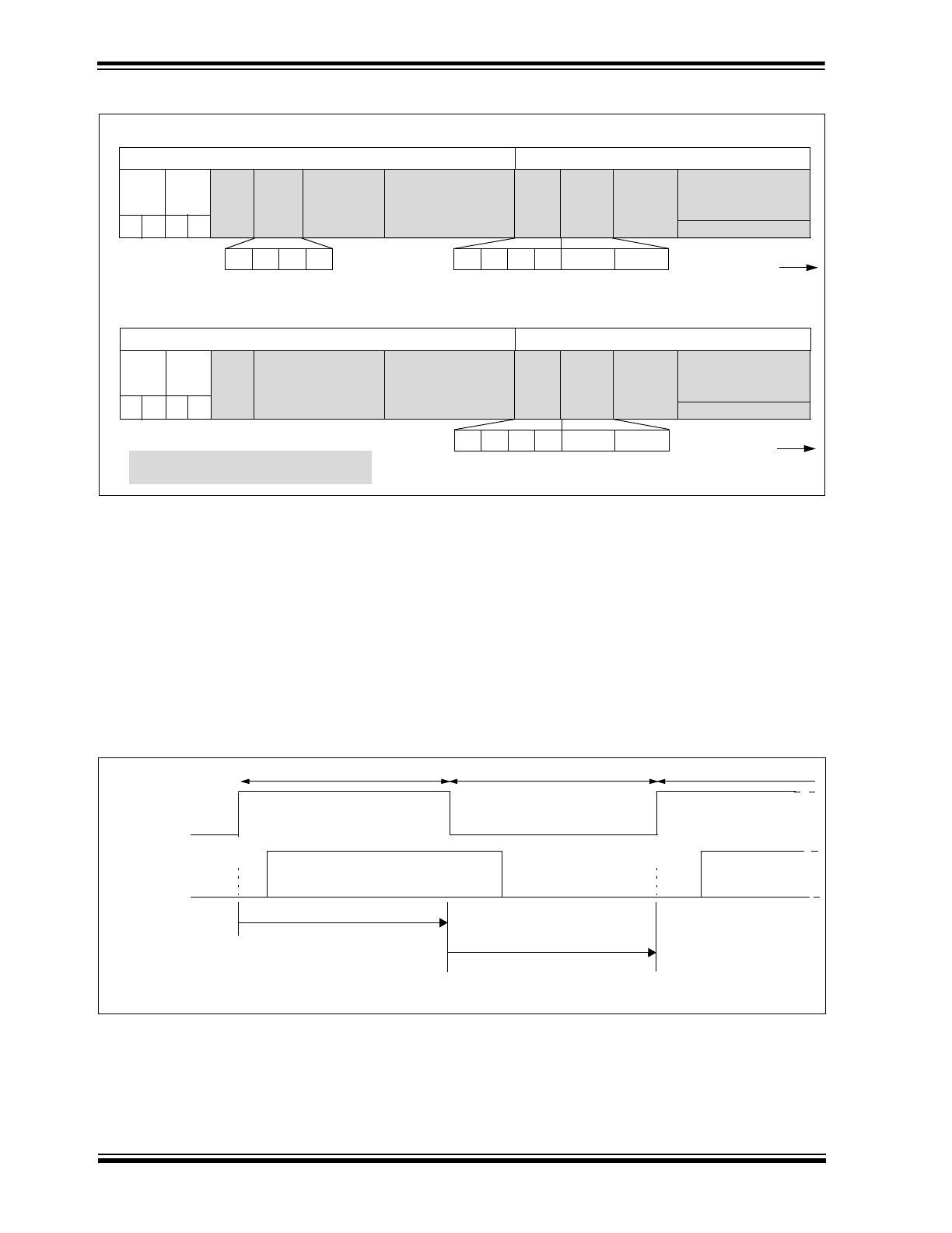
QUEUE COUNTER (QUE)
The QUE counter can be used to request secondary
decoder functions using only a single transmitter but-
ton. Typically a decoder must keep track of incoming
transmissions to determine when a double button press
occurs, perhaps an unlock all doors request. The QUE
counter removes this burden from the decoder by
counting multiple button presses.
The 2-bit QUE counter is incremented each time an
active button input is released for at least the
Debounce Time (T
DBR
), then reactivated (button
pressed again) within the Queue Time (T
QUE
). The
counter increments up from 0 to a maximum of 3,
returning to 0 only after a different button activation or
after button activations spaced greater than the Queue
Time (T
QUE
) apart.
The current transmission aborts, after completing the
minimum number of code words (Section 3.4.1), when
the active button input is released. A button re-activa-
tion within Queue Time (T
QUE
) then initiates a new
transmission (new synchronization counter, encrypted
data) using the updated QUE value.
Figure 3-3 shows the timing diagram to increment the
queue counter value.
FIGURE 3-3:
QUE COUNTER TIMING DIAGRAM
V
LOW
1-Bit
Fixed Code Portion (37 Bits)
QUE
2 Bits
CRC
2 Bits V
LOW
1-Bit
SER 1
Most Sig 16 Bits
SER 0
Least Sig 16 Bits
BUT
4 Bits
Counter
Overflow
2 Bits
DISCRIM
10 Bits
Synchronization
16 Bits
Counter
15
0
S2 S1 S0 LC0 OVR1
OVR0
Hopping Code Portion Message (32 Bits)
Q1 Q0 C1 C0
MSb
LSb
69 Data bits
Transmitted LSb first.
32-bit Serial Number (XSER = 1)
Fixed Code Portion (37 Bits)
QUE
2 Bits
CRC
2 Bits
BUT
4 Bits
S2 S1 S0 LC0
SER 0
Least Sig16 Bits
BUT
4 Bits
Counter
Overflow
2 Bits
DISCRIM
10 Bits
Synchronization
16 Bits
Counter
15
0
S2 S1 S0 LC0 OVR1
OVR0
Hopping Code Portion Message (32 Bits)
Q1 Q0 C1 C0
MSb
LSb
69 Data bits
Transmitted LSb first.
SER 1
12 MSb’s
28-bit Serial Number (XSER = 0)
Shaded data included in CRC calculation
Input
Sx
Code Words
Transmitted
1st Button Press
All Buttons Released
2nd Button Press
QUE1:0 = 00
2
Synch CNT = X
QUE1:0 = 01
2
Synch CNT = X+1
t
2
= 0
t
1
> T
DBP
t
1
= 0
T
DBR
< t < T
QUE