
© 2011 Microchip Technology Inc.
DS40158F-page 1
FEATURES
Security
• Two programmable 64-bit encoder keys
• 16/32-bit bi-directional challenge and response
using one of two keys
• 69-bit transmission length
• 32-bit unidirectional code hopping, 37-bit non-
encrypted portion
• Encoder keys are read protected
• Programmable 28/32-bit serial number
• 60/64-bit, read-protected seed for secure learning
• Three IFF encryption algorithms
• Delayed increment mechanism
• Asynchronous transponder communication
• Queuing information transmitted
Operating
• 2.0V - 6.6V operation, 13V encoder only
operation
• Three switch inputs [S2, S1, S0]—seven functions
• Batteryless bi-directional transponder
• Selectable baud rate and code word blanking
• Automatic code word completion
• Battery low signal transmitted
• Non-volatile synchronization
• PWM or Manchester RF encoding
• Combined transmitter, transponder operation
• Anti-collision of multiple transponders
• Passive proximity activation
• Device protected against reverse battery
• Intelligent damping for high Q LC-circuits
Other
• 37-bit nonencrypted part contains 28/32-bit serial
number, 4/0-bit function code, 1-bit battery low,
2-bit CRC, 2-bit queue
• Simple programming interface
• On-chip tunable RC oscillator (±10%)
• On-chip EEPROM
• 64-bit user EEPROM in transponder mode
• Battery-low LED indication
• SQTP serialization quick-time programming
• 8-pin PDIP/SOIC/TSSOP and die
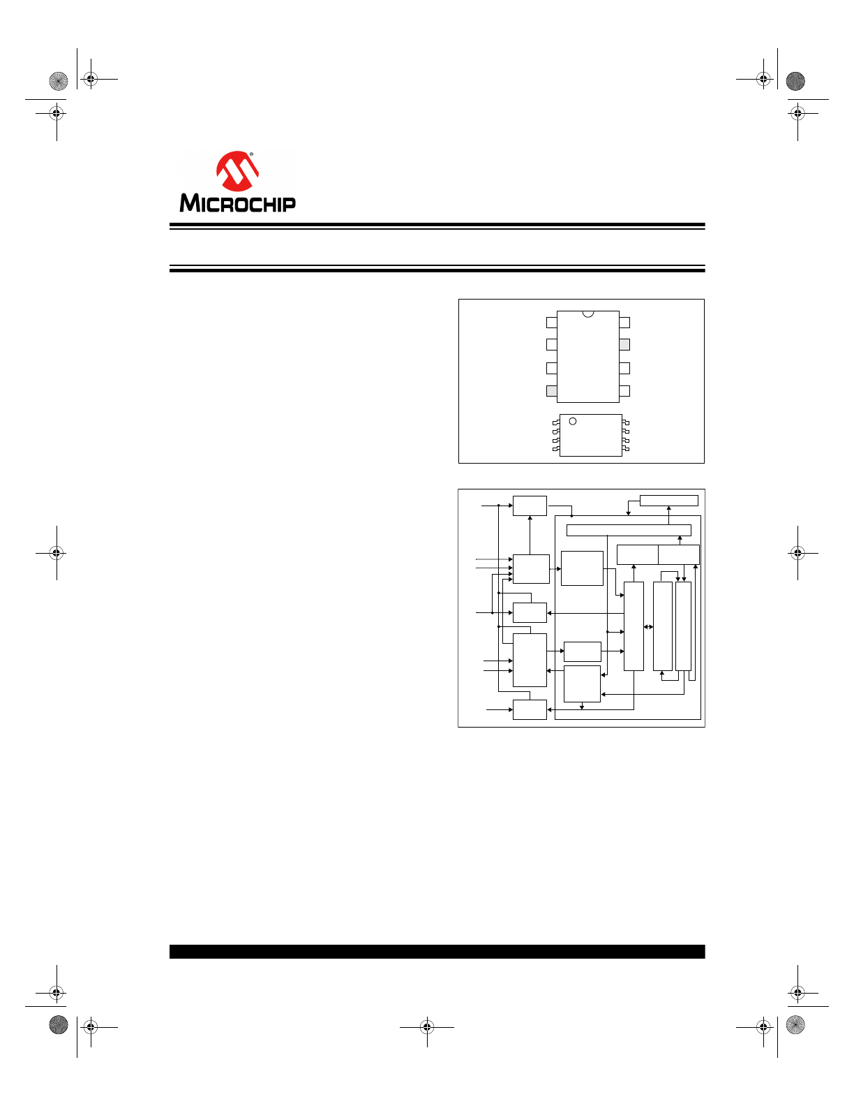
PACKAGE TYPES
BLOCK DIAGRAM
Typical Applications
• Automotive remote entry systems
• Automotive alarm systems
• Automotive immobilizers
• Gate and garage openers
• Electronic door locks (Home/Office/Hotel)
• Burglar alarm systems
• Proximity access control
HCS
410
S0
S1
S2/LED
LC1
V
DD
LC0
PWM
GND
1
8
2
3
4
7
6
5
PDIP, SOIC
HC
S410
S2/LED
LC1
GND
PWM
1
2
3
4
8
7
6
5
S1
S0
V
DD
LC0
TSSOP
Oscillator
Configuration Register
Power
Control
Wake-up
Logic
Address
Decoding EEPROM
Debounce
Control
and
Queuer
LED
Control
PWM
Driver
PPM
Detector
PWM
PPM
Manch.
Encoder
T
ran
spon
der
Cir
c
uit
ry
C
o
nt
ro
l Lo
g
ic
a
nd Coun
ter
s
Encr
ypt
ion/
In
cr
ement
Log
ic
R
egi
st
er
V
DD
S0
S1
S2
LCI0
LCI1
PWM
*Secure Learn patent pending.
HCS410
K
EE
L
OQ
®
Code Hopping Encoder and Transponder
40158F.book Page 1 Wednesday, June 1, 2011 10:36 AM
HCS410
DS40158F-page 2
© 2011 Microchip Technology Inc.
DESCRIPTION
The HCS410 is a code hopping transponder device
designed for secure entry systems. The HCS410 uti-
lizes the patented K
EELOQ®
code hopping system and
bi-directional challenge-and-response for logical and
physical access control. High security learning mecha-
nisms make this a turnkey solution when used with the
K
EELOQ
decoders. The encoder keys and synchroniza-
tion information are stored in protected on-chip
EEPROM.
A low cost batteryless transponder can be imple-
mented with the addition of an inductor and two capac-
itors. A packaged module including the inductor and
capacitor will also be offered.
A single HCS410 can be used as an encoder for
Remote Keyless Entry (RKE) and a transponder for
immobilization in the same circuit and thereby dramat-
ically reducing the cost of hybrid transmitter/transpon-
der circuits.
1.0
SYSTEM OVERVIEW
1.1
Key Terms
• Anti-Collision – Allows two transponders to be in
the files simultaneously and be verified individu-
ally.
• CH Mode – Code Hopping Mode. The HCS410
transmits a 69-bit transmission each time it is acti-
vated, with at least 32-bits changing each time the
encoder is activated.
• Encoder Key – A unique 64-bit key generated and
programmed into the encoder during the manu-
facturing process. The encoder key controls the
encryption algorithm and is stored in EEPROM on
the encoder device.
• IFF – Identify friend or foe is a means of validating
a token. A decoder sends a random challenge to
the token and checks that the response of the
token is a valid response.
• K
EE
L
OQ
Encryption Algorithm – The high security
level of the HCS410 is based on the patented
K
EE
L
OQ
technology. A block cipher encryption
algorithm based on a block length of 32 bits and a
key length of 64 bits is used. The algorithm
obscures the information in such a way that even
if the unencrypted/challenge information differs by
only one bit from the information in the previous
transmission/challenge, the next coded transmis-
sion/response will be totally different. Statistically,
if only one bit in the 32-bit string of information
changes, approximately 50 percent of the coded
transmission will change.
• Learn – The HCS product family facilitates several
learning strategies to be implemented on the
decoder. The following are examples of what can
be done.
Normal Learn –The receiver uses the same infor-
mation that is transmitted during normal operation to
derive the transmitter’s encoder key, decrypt the dis-
crimination value and the synchronization counter.
Secure Learn* – The transmitter is activated through
a special button combination to transmit a stored
60-bit value (random seed) that can be used for key
generation or be part of the key. Transmission of the
random seed can be disabled after learning is com-
pleted.
• Manufacturer’s Code – A 64-bit word, unique to
each manufacturer, used to produce a unique
encoder key in each transmitter (encoder).
• Passive Proximity Activation – When the HCS410
is brought into in a magnetic field without a
command given by the base station, the HCS410
can be programmed to give an RF transmission.
• Transport Code – A 32-bit transport code needs to
be given before the HCS410 can be inductively
programmed. This prevents accidental
programming of the HCS410.
40158F.book Page 2 Wednesday, June 1, 2011 10:36 AM
HCS410
© 2011 Microchip Technology Inc.
DS40158F-page 3
1.2
K
EE
L
OQ
Code Hopping Encoders
When the HCS410 is used as a code hopping encoder
device, it is ideally suited to keyless entry systems,
primarily for vehicles and home garage door openers.
It is meant to be a cost-effective, yet secure solution to
such systems. The encoder portion of a keyless entry
system is meant to be carried by the user and operated
to gain access to a vehicle or restricted area.
Most keyless entry systems transmit the same code
from a transmitter every time a button is pushed. The
relative number of code combinations for a low end
system is also a relatively small number. These
shortcomings provide the means for a sophisticated
thief to create a device that ‘grabs’ a transmission and
retransmits it later or a device that scans all possible
combinations until the correct one is found.
The HCS410 employs the K
EE
L
OQ
code hopping tech-
nology and an encryption algorithm to achieve a high
level of security. Code hopping is a method by which
the code transmitted from the transmitter to the
receiver is different every time a button is pushed. This
method, coupled with a transmission length of 69 bits,
virtually eliminates the use of code ‘grabbing’ or code
‘scanning’.
The HCS410 has a small EEPROM array which must
be loaded with several parameters before use. The
most important of these values are:
• A 28/32-bit serial number which is meant to be
unique for every encoder
• 64-bit seed value
• A 64-bit encoder key that is generated at the time
of production
• A 16-bit synchronization counter value.
• Configuration options
The 16-bit synchronization counter value is the basis
for the transmitted code changing for each transmis-
sion, and is updated each time a button is pressed.
Because of the complexity of the code hopping encryp-
tion algorithm, a change in one bit of the synchroniza-
tion counter value will result in a large change in the
actual transmitted code.
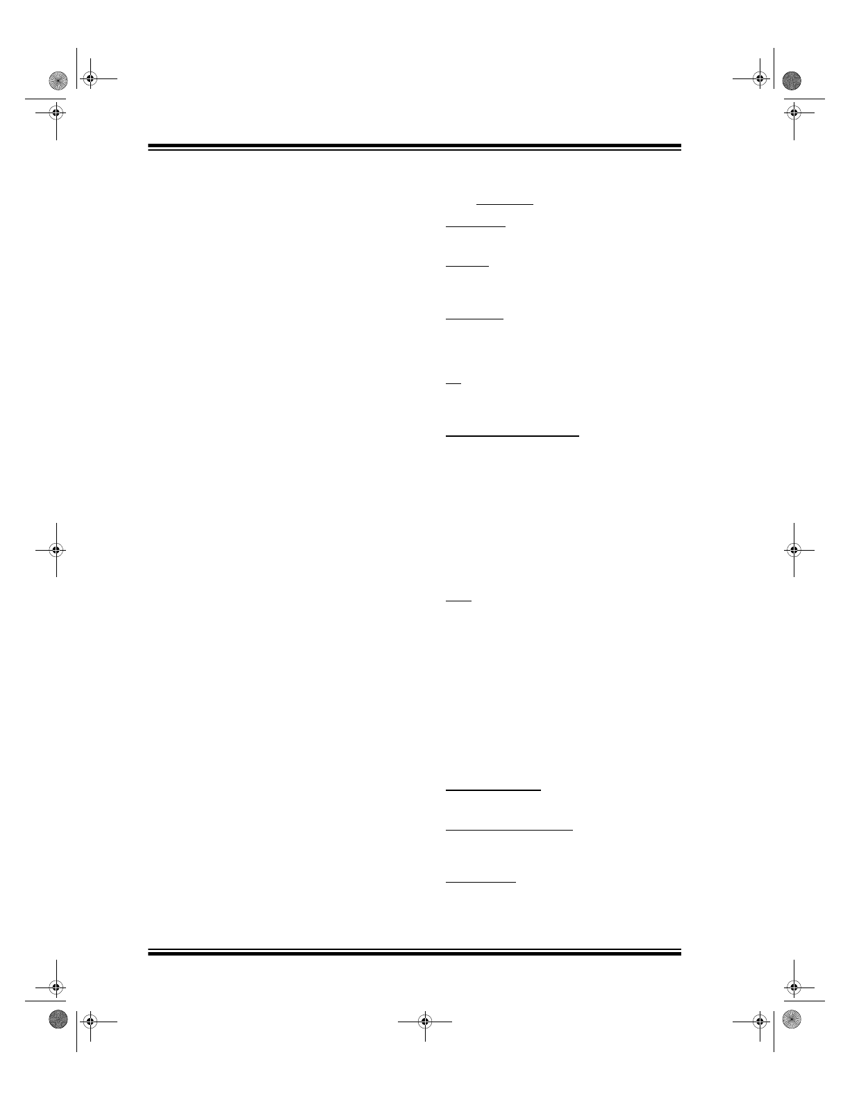
Once the encoder detects that a button has been
pressed, the encoder reads the button and updates the
synchronization counter. The synchronization counter
value, the function bits, and the discrimination value
are then combined with the encoder key in the
encryption algorithm, and the output is 32 bits of
encrypted information (Figure 1-1). The code hopping
portion provides up to four billion changing code com-
binations. This data will change with every button
press, hence, it is referred to as the code hopping
portion of the code word.
The 32-bit code hopping portion is combined with the
button information and the serial number to form the
code word transmitted to the receiver. The code word
format is explained in detail in Section 2.2.
FIGURE 1-1:
BASIC OPERATION OF A CODE HOPPING TRANSMITTER (ENCODER)
K
EE
L
OQ
®
Algorithm
Button Press
Information
Encryption
EEPROM Array
32 Bits of
Encrypted Data
Serial Number
Transmitted Information
Encoder Key
Sync Counter
Serial Number
40158F.book Page 3 Wednesday, June 1, 2011 10:36 AM
HCS410
DS40158F-page 4
© 2011 Microchip Technology Inc.
1.3
K
EE
L
OQ
IFF
The HCS410 can be used as an IFF transponder for
verification of a token. In IFF mode the HCS410 is ide-
ally suited for authentication of a key before disarming
a vehicle immobilizer. Once the key has been inserted
in the car’s ignition the decoder would inductively poll
the key validating it before disarming the immobilizer.
IFF validation of the token involves a random challenge
being sent by a decoder to a token. The token then
generates a response to the challenge and sends this
response to the decoder (Figure 1-2). The decoder cal-
culates an expected response using the same chal-
lenge. The expected response is compared to the
response received from the token. If the responses
match, the token is identified as a valid token and the
decoder can take appropriate action.
The HCS410 can do either 16 or 32-bit IFF. The
HCS410 has two encryption algorithms that can be
used to generate a response to a challenge. In addition
there are up to two encoder keys that can be used by
the HCS410. Typically each HCS410 will be pro-
grammed with a unique encoder key(s).
In IFF mode, the HCS410 will wait for a command from
the base station and respond to the command. The
command can either request a read/write from user
EEPROM or an IFF challenge response. A given 16 or
32-bit challenge will produce a unique 16/32-bit
response, based on the IFF key and IFF algorithm
used.
FIGURE 1-2:
BASIC OPERATION OF AN IFF TOKEN
IFF Key
Serial Number
K
EE
L
OQ
®
IFF
Algorithm
Serial Number
EEPROM Array
Challenge Received from Decoder
Response
Read by Decoder
40158F.book Page 4 Wednesday, June 1, 2011 10:36 AM
HCS410
© 2011 Microchip Technology Inc.
DS40158F-page 5
2.0
DEVICE OPERATION
The HCS410 can either operate as a normal code hop-
ping transmitter with one or two IFF keys (Figure 2-1)
or as purely an IFF token with two IFF keys (Figure 2-2
and Figure 2-3). When used as a code hopping trans-
mitter the HCS410 only needs the addition of buttons
and RF circuitry for use as a transmitter. Adding the
transponder function to the transmitter requires the
addition of an inductor and two capacitors as shown in
Figure 2-1 and Figure 2-2. A description of each pin is
given in Table 2-1. Table 2-2 shows the function codes
for using the HCS410.
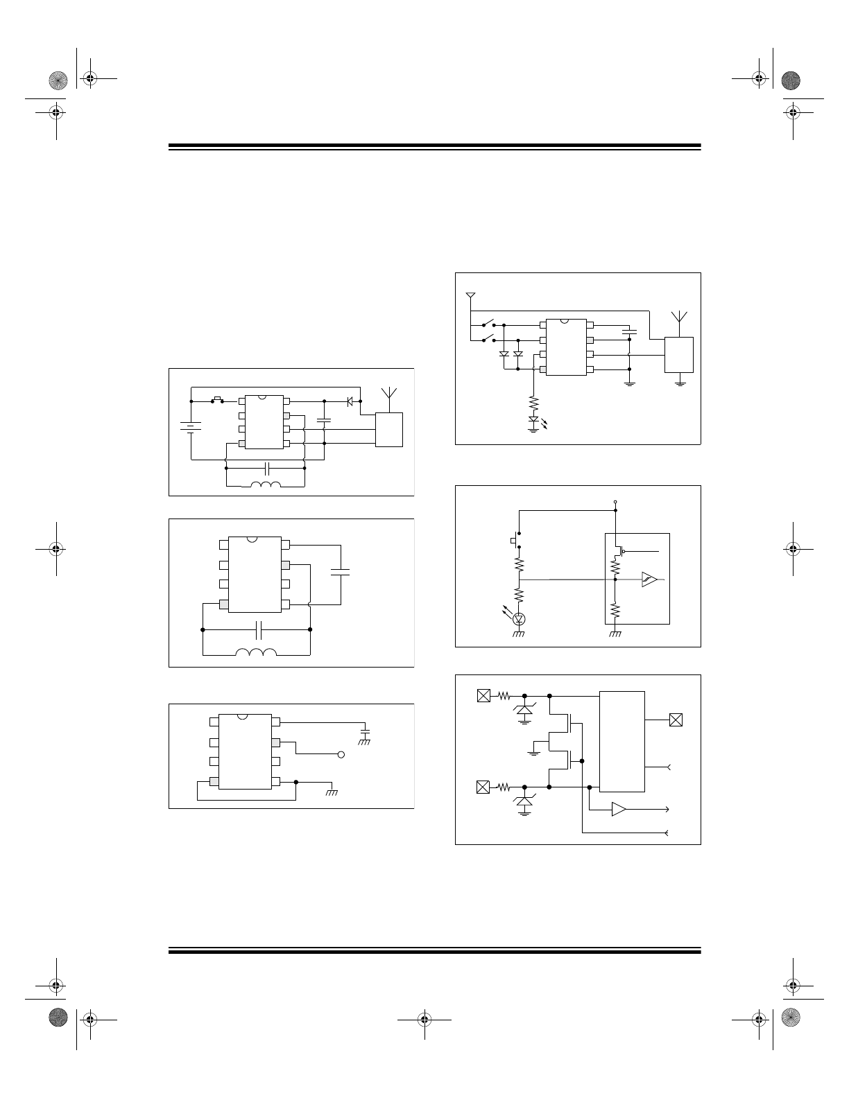
FIGURE 2-1:
COMBINED TRANSMITTER/
TRANSPONDER CIRCUIT
FIGURE 2-2:
TRANSPONDER CIRCUIT
FIGURE 2-3:
2-WIRE, 1 OR 2-KEY IFF
TOKEN
Figure 2-4 shows how to use the HCS410 with a 12V
battery as a code hopping transmitter. The circuit uses
the internal regulator, normally used for charging a
capacitor/battery in LC mode, to generate a 6V supply
for the HCS410.
FIGURE 2-4:
HCS410 ENCODER WITH 12V
BATTERY
FIGURE 2-5:
LED CONNECTION TO
S2/LED OUTPUT
FIGURE 2-6:
LC PIN BLOCK DIAGRAM
1
8
RF
2
3
4
7
6
5
1 µF
1
8
2
3
4
7
6
5
1 µF
1
8
2
3
4
7
6
5
1 µF
Data I/O
1
8
RF
2
3
4
7
6
5
6.3V
12V
Pulse
V
DD
S2/LED
220
Ω
220
Ω
60k
30
Ω
V
DD
6.3V
Damp
Out
MOD
Detector
Rectifier,
Damping,
Clamping
15V
15V
100
Ω
100
Ω
LC1
LC0
40158F.book Page 5 Wednesday, June 1, 2011 10:36 AM
HCS410
DS40158F-page 6
© 2011 Microchip Technology Inc.
2.1
Pinout Description
The HCS410 has the same footprint as all of the other
devices in the K
EE
L
OQ
family, except for the two pins
that are reserved for transponder operations and the
LED that is now located at the same position as the S2
switch input.
• S[0:1] – are inputs with Schmitt Trigger detectors
and an internal 60k¾ (nominal) pull-down
resistors.
• S2/LED – uses the same input detection circuit as
S0/S1 but with an added PMOS transistor con-
nected to V
DD
capable of sourcing enough current
to drive an LED.
• LC[0:1] – is the transponder interface pins to be
connected to an LC circuit for inductive communi-
cation. LC0 is connected to a detector for data
input. Data output is achieved by clamping LC0
and LC1 to GND through two NMOS transistors.
These pins are also connected to a rectifier and a
regulator, providing power to the rest of the logic
and for charging an external power source (Bat-
tery/Capacitor) through V
DD
.
The input impedance of the LC pins is a function of
input voltage. At low voltages, the input impedance is
in the order of mega-ohms. When laying out a PC
board, care should be taken to ensure that there
is no cross coupling between the LC pins and
other traces on the board. Glitches on the LC lines
will cause the device to reset. A high-value resistor
(220 KW) between LC0 and GND can be added to
reduce sensitivity.
TABLE 2-1:
PINOUT DESCRIPTION
Name
Pin Number
Description
S0
1
Switch input 0
S1
2
Switch input 1
S2/LED
3
Switch input 2/LED output, Clock pin for programming mode
LC1
4
Transponder interface pin
V
SS
5
Ground reference connection
PWM
6
Pulse width modulation (PWM)
output pin/Data pin for
programming mode
LC0
7
Transponder interface pin
V
DD
8
Positive supply voltage connection
TABLE 2-2:
FUNCTION CODES
LC0
S2
S1
S0
Comments
1
0
0
0
1
Normal Code Hopping transmission
2
0
0
1
0
Normal Code Hopping transmission
3
0
0
1
1
Delayed seed transmission if allowed by SEED and TMPSD/Normal
Code Hopping transmission
4
0
1
0
0
Normal Code Hopping transmission
5
0
1
0
1
Normal Code Hopping transmission
6
0
1
1
0
Normal Code Hopping transmission
7
0
1
1
1
Immediate seed transmission if allowed by SEED and TMPSD/Normal
Code Hopping transmission
8
1
0
0
0
Transponder mode
40158F.book Page 6 Wednesday, June 1, 2011 10:36 AM
HCS410
© 2011 Microchip Technology Inc.
DS40158F-page 7
2.2
Code Hopping Mode (CH Mode)
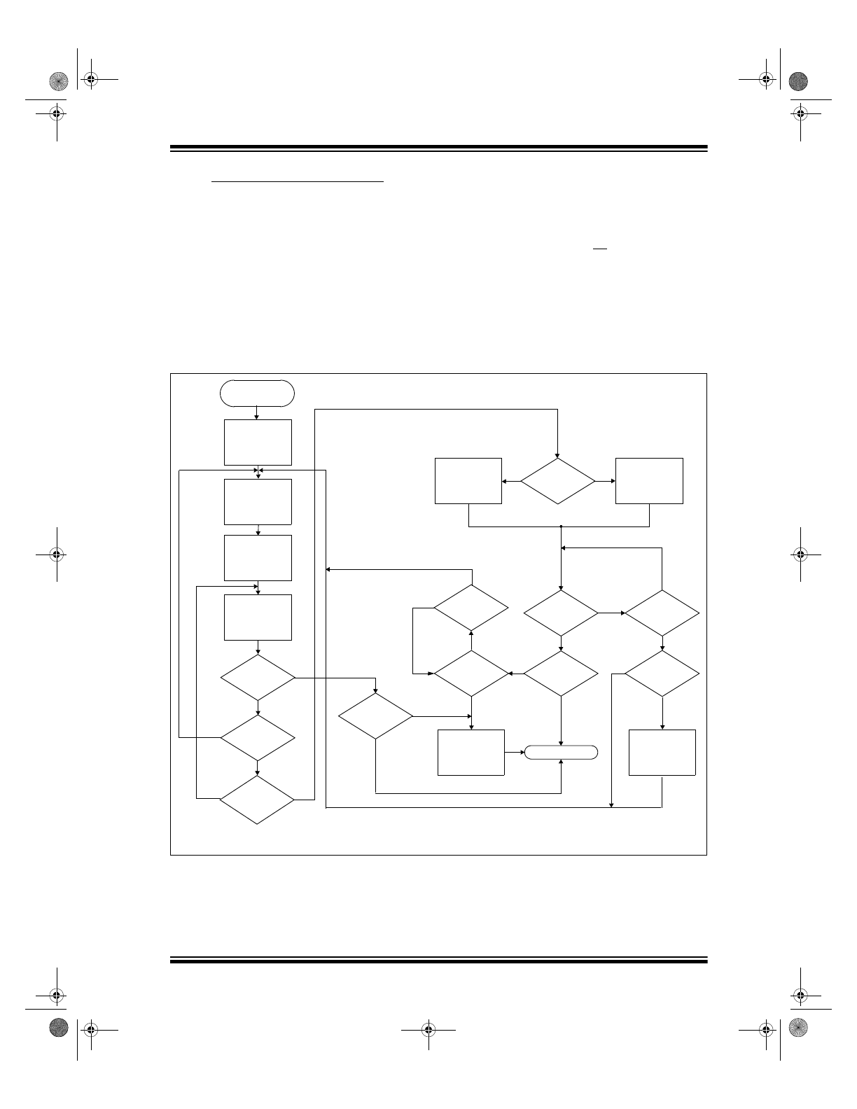
The HCS410 wakes up upon detecting a switch closure
and then delays approximately 30 ms for switch
debounce (Figure 2-7). The synchronization counter
value, fixed information, and switch information are
encrypted to form the code hopping portion. The
encrypted or code hopping portion of the transmission
changes every time a button is pressed, even if the
same button is pushed again. Keeping a button
pressed for a long time results in the same code word
being transmitted until the button is released or time-
out occurs. A code that has been transmitted will not
occur again for more than 64K transmissions. Overflow
information programmed into the encoder can be used
by the decoder to extend the number of unique trans-
missions to more than 192K.
If, during the transmit process, it is detected that a new
button(s) has been added, a reset will immediately be
forced and the code word will not be completed. Please
note that buttons removed will not have any effect on
the code word unless no buttons remain pressed in
which case the current code word will be completed
and the power down will occur. If, after a button combi-
nation is pressed, and the same button combination is
pressed again within 2 seconds of the first press, the
current transmission will be aborted and a new trans-
FIGURE 2-7:
CODE HOPPING ENCODER OPERATION
20-second
time-out
No
Transmitted
2 second
time-out
completed?
All buttons
released?
Sample Inputs
Update Sync Info
Encrypt With
Transmit
Encoder Key
Power-up
(A button has been
pressed (Note1))
Buttons added?
Yes
Yes
Yes
No
(Note 1)
7 complete code
words?
Complete current
code word while
checking buttons
(Note 2)
Stop transmitting
DINC Set?
Power down
Buttons
pressed?
(Note 1)
Same as
previous
press?
Increment queue
counter
20 second
time-out
completed?
Buttons
pressed?
(Note 1)
Increase sync
counter
by 12
immediately
Yes
Yes
No
Yes
Yes
No
No
No
Yes
No
Yes
No
No
Note 1: 30 ms debounce on press and release of all buttons.
2: Completes a minimum of 3 code words if MTX3 is set.
No
DINC
Set?
Yes
Yes
No
40158F.book Page 7 Wednesday, June 1, 2011 10:36 AM
HCS410
DS40158F-page 8
© 2011 Microchip Technology Inc.
2.2.1
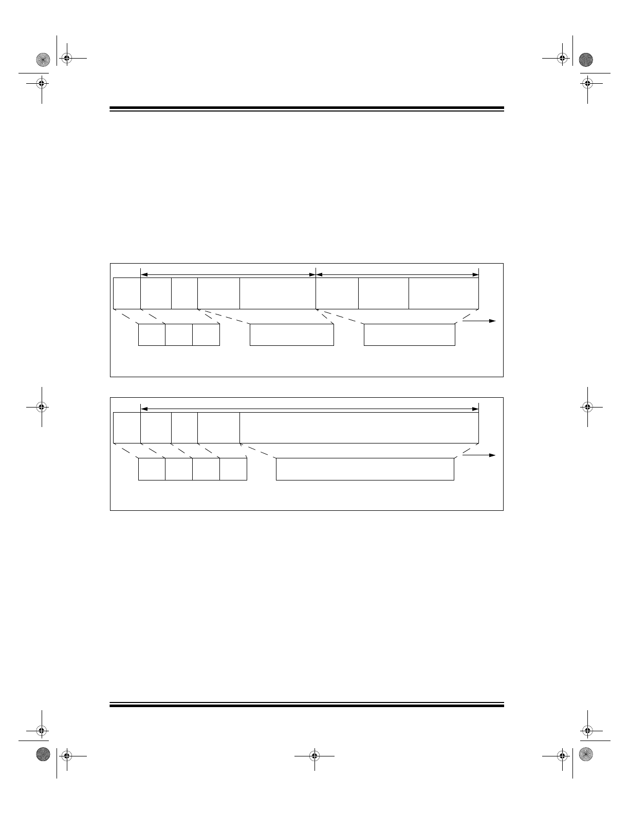
TRANSMISSION DATA FORMAT
The HCS410 transmission (CH Mode) is made up of
several parts (Figure 2-10 and Figure 2-11). Each
transmission is begun with a preamble and a header,
followed by the encrypted and then the fixed data. The
actual data is 69 bits which consists of 32 bits of
encrypted data and 37 bits of fixed data. Each trans-
mission is followed by a guard period before another
transmission can begin. Refer to Table 6-4
and Table 6-5 for transmission timing specifications.
The combined encrypted and nonencrypted sections
increase the number of combinations to 1.47 x 10
20
.
The HCS410 transmits a 69-bit code word when a but-
ton is pressed. The 69-bit word is constructed from a
Fixed Code portion and Code Hopping portion
(Figure 2-8).
The Encrypted Data is generated from 4 function bits,
2 overflow bits, and 10 discrimination bits, and the 16-
bit synchronization counter value (Figure 2-8).
The Nonencrypted Code Data is made up of 2 QUE
bits, 2 CRC bits, a V
LOW
bit, 4 function bits, and the
28-bit serial number. If the extended serial number
(32 bits) is selected, the 4 function code bits will not be
transmitted (Figure 2-8).
FIGURE 2-8:
HOP CODE WORD ORGANIZATION (RIGHT-MOST BIT IS CLOCKED OUT FIRST)
FIGURE 2-9:
SEED CODE WORD ORGANIZATION
Fixed Code Data
Encrypted Code Data
69 bits
of Data
Transmitted
MSB
LSB
CRC
(2 bit)
V
LOW
(1 bit)
Button
Status*
(4 bits)
28-bit
Serial Number
Overflow (2 bits)
bits (10 bits)
16-bit
Synchronization
CRC
(2 bits)
V
LOW
(1 bit)
+
Serial Number and
Button Status (32 bits)
+
32 bits of Encrypted Data
QUE
QUE
(Q1, Q0
S2 S1 S0 0
Button
Status
(4 bits)
S2 S1 S0 0
(2 bits)
bit)
Counter Value
Discrimination
and
* Optional.
Fixed Code Data
69 bits
of Data
Transmitted
CRC
(2 bit)
V
LOW
(1 bit)
Button*
Status
(4 bits)
CRC
(2 bits)
V
LOW
(1 bit)
+
QUE
QUE0
(Q1, Q0
S2 S1 S0 0
(2 bits)
bit)
Unencrypted
Button
(4 bits)
SEED
(60 bits)
+
SEED
* Optional.
40158F.book Page 8 Wednesday, June 1, 2011 10:36 AM
HCS410
© 2011 Microchip Technology Inc.
DS40158F-page 9
2.2.2
TRANSMISSION DATA MODULE
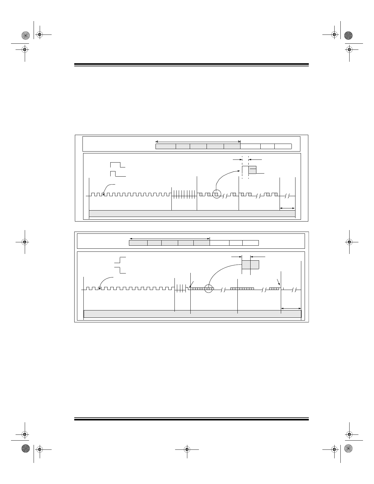
The Data Modulation Format is selectable between
Pulse Width Modulation (PWM) format and Manchester
encoding. Both formats are preceded by a preamble
and synchronization header, followed by the 69-bits of
data. Manchester encoding has a leading and closing
‘1’ for each code word.
The same code word is continuously sent as long as
the input pins are kept high with a guard time separat-
ing the code words. All of the timing values are in mul-
tiples of a Basic Timing Element (T
E
), which can be
changed using the baud rate option bits.
FIGURE 2-10: TRANSMISSION FORMAT—MANCH = 0
FIGURE 2-11: TRANSMISSION FORMAT—MANCH = 1
LOGIC "1"
Code Word
Guard
Time
Preamble
Sync
Encrypted
TX Data
Fixed Code
BIT
LOGIC "0"
1
2
3 5 7 9
4 6 8 10
T
E
CODE WORD:
TOTAL TRANSMISSION:
Preamble Sync Encrypt
Fixed
Guard
1 CODE WORD
1 2
4 5
6
Preamble Sync
Encrypt
14 15 16
T
E
Data
T
E
Guard
Preamble
Sync
Encrypted
Fixed Code
LOGIC "0"
1
2
3
4
T
E
CODE WORD:
TOTAL TRANSMISSION:
Sync
Encrypt
Fixed
Guard
1 CODE WORD
1
2
4
5
6
Preamble
Sync
Encrypt
14 15 16
LOGIC "1"
Start bit
Stop bit
CODE WORD
Preamble
Time
Data
Data
40158F.book Page 9 Wednesday, June 1, 2011 10:36 AM
HCS410
DS40158F-page 10
© 2011 Microchip Technology Inc.
2.3
Code Hopping Mode Special Features
2.3.1
CODE WORD COMPLETION
Code word completion is an automatic feature that
ensures that the entire code word is transmitted, even
if the button is released before the transmission is com-
plete. The HCS410 encoder powers itself up when a
button is pushed and powers itself down after the com-
mand is finished (Figure 2-7). If MTX3 is set in the con-
figuration word, a minimum of three transmissions will
be transmitted when the HCS410 is activated, even if
the buttons are released.
If less than seven words have been transmitted when
the buttons are released, the HCS410 will complete the
current word. If more than seven words have been
transmitted, and the button is released, the PWM out-
put is immediately switched off.
2.3.2
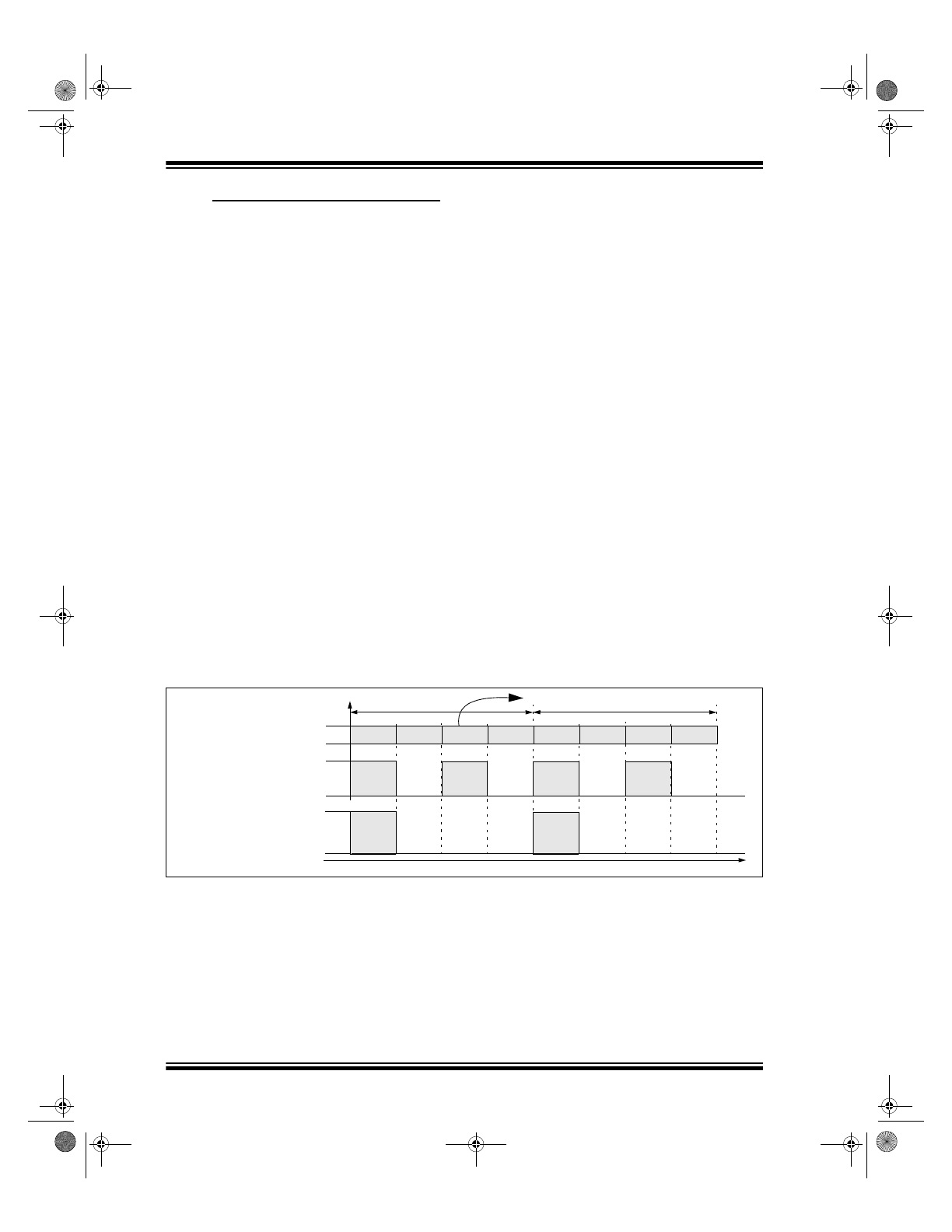
CODE WORD BLANKING ENABLE
Federal Communications Commission (FCC) part 15
rules specify the limits on fundamental power and
harmonics that can be transmitted. Power is calculated
on the worst case average power transmitted in a
100ms window. It is therefore advantageous to
minimize the duty cycle of the transmitted word. This
can be achieved by minimizing the duty cycle of the
individual bits and by blanking out consecutive words.
Code Word Blanking Enable (CWBE) is used for
reducing the average power of a transmission
(Figure 2-12). Using the CWBE allows the user to
transmit a higher amplitude transmission if the
transmission length is shorter. The FCC puts
constraints on the average power that can be
transmitted by a device, and CWBE effectively
prevents continuous transmission by only allowing the
transmission of every second or fourth word. This
reduces the average power transmitted and hence,
assists in FCC approval of a transmitter device.
The HCS410 will either transmit all code words, 1 in 2
or 1 in 4 code words, depending on the baud rate
selected and the code word blanking option. See
Section 3.7 for additional details.
2.3.3
CRC (CYCLE REDUNDANCY CHECK) BITS
The CRC bits are calculated on the 65 previously trans-
mitted bits. The CRC bits can be used by the receiver
to check the data integrity before processing starts. The
CRC can detect all single bit and 66% of double bit
errors. The CRC is computed as follows:
EQUATION 2-1:
CRC CALCULATION
and
with
and Di
n
the nth transmission bit 0 ð n ð 64
FIGURE 2-12: CODE WORD BLANKING ENABLE
CRC 1
[ ]
n 1
+
CRC 0
[ ]
n
Di
n
⊕
=
CRC 0
[ ]
n 1
+
CRC 0
[ ]
n
Di
n
⊕
(
)
CRC 1
[ ]
n
⊕
=
CRC 1 0
,
[
]
0
0
=
One Code Word
CWBE Disabled
(All words transmitted)
CWBE Enabled
(1 out of 2 transmitted)
A
2A
Amplitude
CWBE Enabled
(1 out of 4 transmitted)
4A
Time
•Patents have been applied for.
40158F.book Page 10 Wednesday, June 1, 2011 10:36 AM