
2011 Microchip Technology Inc.
DS41111E-page 1
K
EE
L
OQ®
Code Hopping Encoder
FEATURES
Security
• Two programmable 32-bit serial numbers
• Two programmable 64-bit encoder keys
• Two programmable 60-bit seed values
• Each transmission is unique
• 67/69-bit transmission code length
• 32-bit hopping code
• Crypt keys are read protected
Operating
• 2.05-5.5V operation
• Six button inputs
• 15 functions available
• Four selectable baud rates
• Selectable minimum code word completion
• Battery low signal transmitted to receiver
• Nonvolatile synchronization data
• PWM, VPWM, PPM, and Manchester modulation
• Button queue information transmitted
• Dual Encoder functionality
Other
• On-chip EEPROM
• On-chip tuned oscillator (±10% over voltage and
temperature)
• Button inputs have internal pull-down resistors
• LED output
• PLL control for ASK and FSK
• Low external component count
• Step-up voltage regulator
Typical Applications
The HCS370 is ideal for Remote Keyless Entry (RKE)
applications. These applications include:
• Automotive RKE systems
• Automotive alarm systems
• Automotive immobilizers
• Gate and garage door openers
• Identity tokens
• Burglar alarm systems
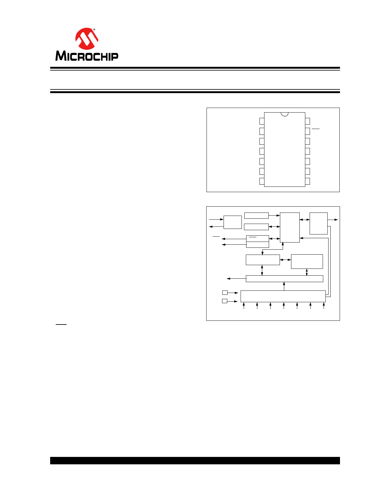
PACKAGE TYPES
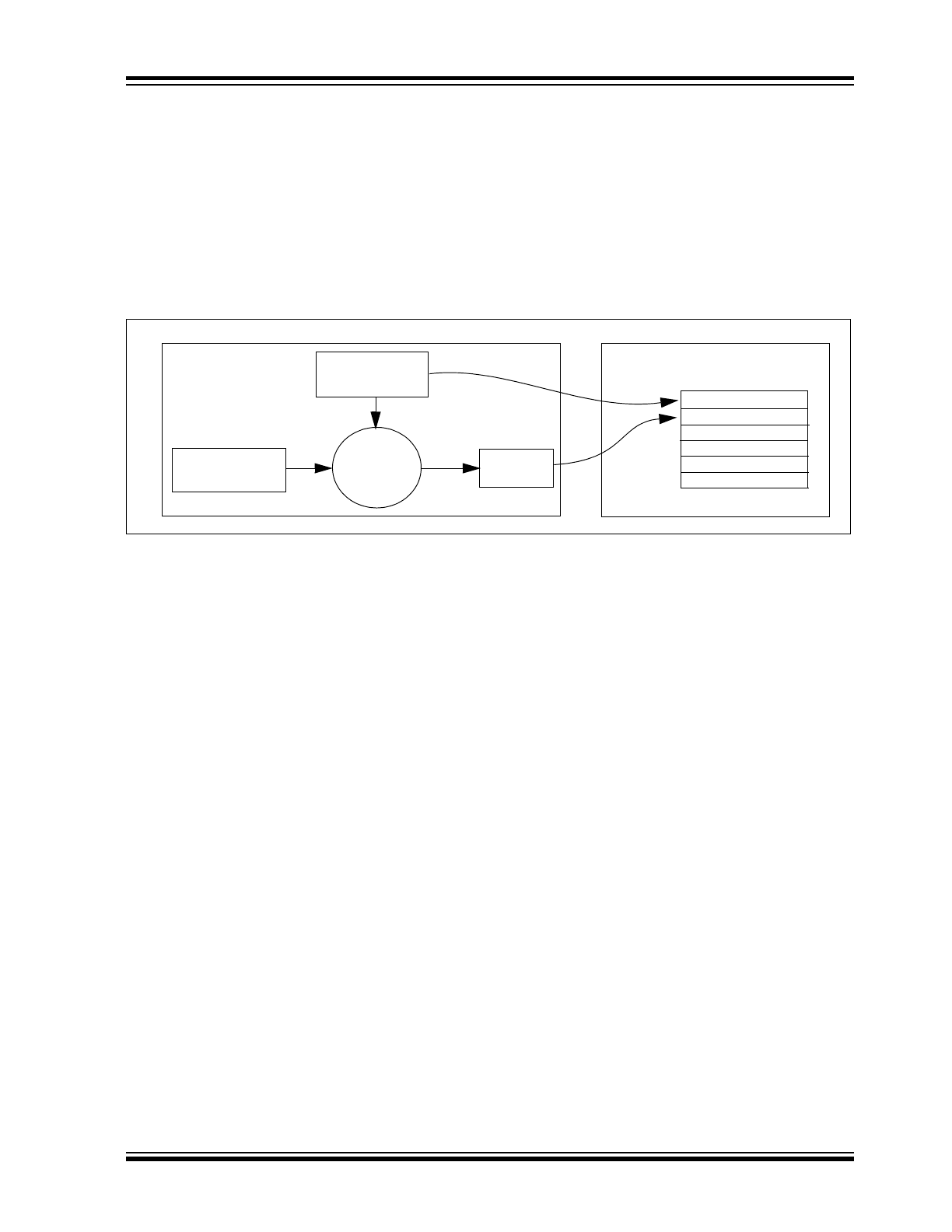
HCS370 BLOCK DIAGRAM
GENERAL DESCRIPTION
The HCS370 is a code hopping encoder designed for
secure Remote Keyless Entry (RKE) and secure
remote control systems. The HCS370 utilizes the
K
EE
L
OQ®
code hopping technology, which incorpo-
rates high security, a small package outline, and low
cost to make this device a perfect solution for unidirec-
tional authentication systems and access control sys-
tems.
The HCS370 combines a hopping code generated by a
nonlinear encryption algorithm, a serial number, and
status bits to create a secure transmission code. The
length of the transmission eliminates the threat of code
scanning and code grabbing access techniques.
8
14
1
2
3
4
13
12
11
S0
S1
S2
S3
V
DD
LED
DATA
Vss
PDIP, SOIC,
H
C
S370
S4
SLEEP/S5
SHIFT
RFEN
STEP
V
IN
5
6
7
10
9
TSSOP
V
SS
V
DD
Oscillator
RESET circuit
LED driver
Controller
Power
latching
and
switching
Button input port
32-bit SHIFT register
Encoder
EEPROM
DATA
LED
S3
S2
S
1
S
0
S4
S5
SHIFT
RF Enable
RFEN
Step-up
regulator
STEP
V
IN
SLEEP
HCS370

HCS370
DS41111E-page 2
2011 Microchip Technology Inc.
The crypt key, serial number, and configuration data
are stored in an EEPROM array which is not accessible
via any external connection. The EEPROM data is pro-
grammable but read protected. The data can be veri-
fied only after an automatic erase and programming
operation. This protects against attempts to gain
access to keys or manipulate synchronization values.
In addition, the HCS370 supports a dual encoder. This
allows two manufacturers to use the same device with-
out having to use the same manufacturer’s code in
each of the encoders. The HCS370 provides an easy
to use serial interface for programming the necessary
keys, system parameters, and configuration data.
1.0
SYSTEM OVERVIEW
Key Terms
The following is a list of key terms used throughout this
data sheet. For additional information on K
EE
L
OQ
and
code hopping, refer to Technical Brief (TB003).
• RKE - Remote Keyless Entry
• Button Status - Indicates what button input(s)
activated the transmission. Encompasses the 6
button status bits S5, S4, S3, S2, S1 and S0
(Figure 3-2).
• Code Hopping - A method by which a code,
viewed externally to the system, appears to
change unpredictably each time it is transmitted.
• Code Word - A block of data that is repeatedly
transmitted upon button activation (Figure 3-2).
• Transmission - A data stream consisting of
repeating code words (Figure 4-1).
• Crypt Key - A unique and secret 64-bit number
used to encrypt and decrypt data. In a symmetri-
cal block cipher such as the K
EE
L
OQ
algorithm,
the encryption and decryption keys are equal and
will therefore be referred to generally as the crypt
key.
• Encoder - A device that generates and encodes
data.
• Encryption Algorithm - A recipe whereby data is
scrambled using a crypt key. The data can only be
interpreted by the respective decryption algorithm
using the same crypt key.
• Decoder - A device that decodes data received
from an encoder (i.e., HCS5XX).
• Decryption Algorithm - A recipe whereby data
scrambled by an encryption algorithm can be
unscrambled using the same crypt key.
• Learn – Learning involves the receiver calculating
the transmitter’s appropriate crypt key, decrypting
the received hopping code and storing the serial
number, synchronization counter value, and crypt
key in EEPROM. The K
EE
L
OQ
product family facil-
itates several learning strategies to be imple-
mented on the decoder. The following are
examples of what can be done.
- Simple Learning
The receiver uses a fixed crypt key. The crypt
key is common to every component used by
the same manufacturer.
- Normal Learning
The receiver derives a crypt key from the
encoder serial number. Every transmitter has
a unique crypt key.
- Secure Learning
The receiver derives a crypt key from the
encoder seed value. Every encoder has a
unique seed value that is only transmitted by
a special button combination.
• Manufacturer’s Code – A unique and secret 64-
bit number used to derive crypt keys. Each
encoder is programmed with a crypt key that is a
function of the manufacturer’s code. Each
decoder is programmed with the manufacturer
code itself.
The HCS370 code hopping encoder is designed specif-
ically for keyless entry systems. In particular, typical
applications include vehicles and home garage door
openers. The encoder portion of a keyless entry sys-
tem is integrated into a transmitter carried by the user.
The transmitter is operated to gain access to a vehicle
or restricted area. The HCS370 is meant to be a cost-
effective yet secure solution to such systems requiring
very few external components (Figure 2-1).
Most low end keyless entry transmitters are given a
fixed identification code that is transmitted every time a
button is pushed. The number of unique identification
codes in a low end system is usually a relatively small
number. These shortcomings provide an opportunity
for a sophisticated thief to create a device that ‘grabs’
a transmission and retransmits it later or a device that
quickly ‘scans’ all possible identification codes until the
correct one is found.
The HCS370, on the other hand, employs the K
EE
L
OQ
code hopping technology coupled with a transmission
length of 67 bits to virtually eliminate the use of code
‘grabbing’ or code ‘scanning’. The high security level of
the HCS370 is based on the patented K
EE
L
OQ
technol-
ogy. A block cipher based on a block length of 32 bits
and a key length of 64 bits is used. The algorithm
obscures the information in such a way that if a single
hopping code data bit changes (before encryption), sta-
tistically more than 50% of the encrypted data bits will
change.
2011 Microchip Technology Inc.
DS41111E-page 3
HCS370
As indicated in the block diagram on page one, the
HCS370 has a small EEPROM array which must be
loaded with several parameters before use; most often
programmed by the manufacturer at the time of produc-
tion. The most important of these are:
• A serial number, typically unique for every
encoder
• A crypt key
• An initial synchronization value
The crypt key generation typically inputs the transmitter
serial number and 64-bit manufacturer’s code into the
key generation algorithm (Figure 1-1). The manufac-
turer’s code is chosen by the system manufacturer and
must be carefully controlled as it is a pivotal part of the
overall system security.
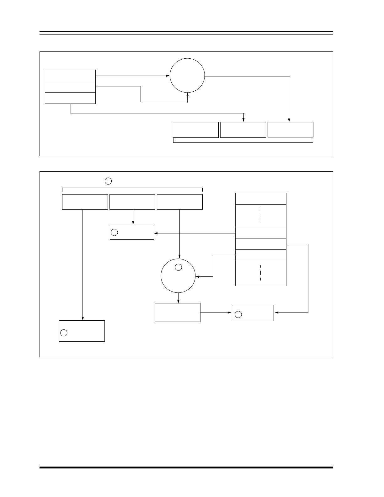
FIGURE 1-1:
CREATION AND STORAGE OF CRYPT KEY DURING PRODUCTION
The synchronization counter is the basis behind the
transmitted code word changing for each transmission;
it increments each time a button is pressed. Each incre-
ment of the synchronization value results in more than
50% of the hopping code bits changing.
Figure 1-2 shows how the key values in EEPROM are
used in the encoder. Once the encoder detects a button
press, it reads the button inputs and updates the syn-
chronization counter. The synchronization counter and
crypt key are input to the encryption algorithm and the
output is 32 bits of encrypted information. This data will
change with every button press while its value will
appear to ‘randomly hop around’. Hence, this data is
referred to as the hopping portion of the code word.
The 32-bit hopping code is combined with the button
information and serial number to form the code word
transmitted to the receiver. The code word format is
explained in greater detail in Section 4.1.
A receiver may use any type of controller as a decoder.
Typically, it is a microcontroller with compatible firm-
ware that allows the decoder to operate in conjunction
with an HCS370 based transmitter.
A transmitter must first be ‘learned’ by the receiver
before its use is allowed in the system. Learning
includes calculating the transmitter’s appropriate crypt
key, decrypting the received hopping code, storing the
serial number, storing the synchronization counter
value, and storing crypt key in EEPROM.
In normal operation, each received message of valid
format is evaluated. The serial number is used to deter-
mine if it is from a learned transmitter. If the serial num-
ber is from a learned transmitter, the message is
decrypted and the synchronization counter is verified.
Finally, the button status is checked to see what opera-
tion is requested. Figure 1-3 shows the relationship
between some of the values stored by the receiver and
the values received from the transmitter.
For detailed decoder operation, see Section 7.0.
Transmitter
Manufacturer’s
Serial Number
Code
Crypt
Key
Key
Generation
Algorithm
Serial Number
Crypt Key
Sync Counter
.
.
.
HCS370
Production
Programmer
EEPROM Array
HCS370
DS41111E-page 4
2011 Microchip Technology Inc.
FIGURE 1-2:
BUILDING THE TRANSMITTED CODE WORD (ENCODER)
FIGURE 1-3:
BASIC OPERATION OF RECEIVER (DECODER)
NOTE: Circled numbers indicate the order of execution.
Button Press
Information
EEPROM Array
32 Bits
Encrypted Data
Serial Number
Transmitted Information
Crypt Key
Sync Counter
Serial Number
K
EE
L
OQ®
Encryption
Algorithm
Button Press
Information
EEPROM Array
Manufacturer Code
32 Bits of
Encrypted Data
Serial Number
Received Information
Decrypted
Synchronization
Counter
Verify
Counter
Sync Counter
Serial Number
K
EE
L
OQ®
Decryption
Algorithm
1
3
4
Check for
Match
2
Perform Function
Indicated by
button press
5
Crypt Key
B0
B1
2011 Microchip Technology Inc.
DS41111E-page 5
HCS370
2.0
DEVICE DESCRIPTION
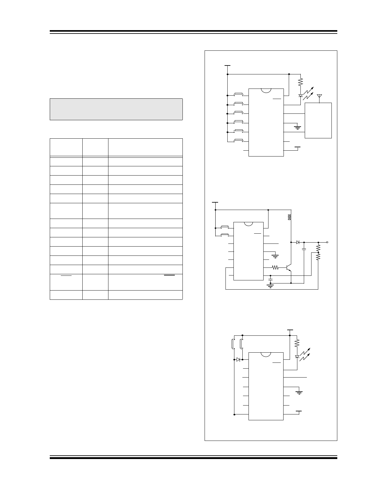
As shown in the typical application circuits (Figure 2-1),
the HCS370 is an easy device to use. It requires only
the addition of buttons and RF circuitry for use as the
encoder in your security application. A description of
each pin is described in Table 2-1. Refer to Figure 2-3
for information on the I/O pins.
TABLE 2-1:
PIN DESCRIPTIONS
The HCS370 will normally be in a low power SLEEP
mode. When a button input is taken high, the device will
wake-up, start the step-up regulator, and go through
the button debounce delay of T
DB
before the button
code is latched. In addition, the device will then read
the configuration options. Depending on the configura-
tion options and the button code, the device will deter-
mine what the data and modulation format will be for
the transmission. The transmission will consist of a
stream of code words and will be transmitted T
PU
after
the button is pressed for as long as the buttons are held
down or until a time-out occurs. The code word format
can be either a code hopping format or a seed format.
The time-out time can be selected with the Time-out
Select (TSEL) configuration option. This option allows
the time-out to be set to 0.8s, 3.2s, 12.8s, or 25.6s.
When a time-out occurs, the device will go into SLEEP
mode to protect the battery from draining when a button
gets stuck. This option must be chosen to meet maxi-
mum transmission length regulatory limits which vary
by country.
FIGURE 2-1:
TYPICAL CIRCUITS
Note:
S0-S5 and SHIFT inputs have pull-down
resistors. V
IN
should be tied high if the
step-up regulator is not used.
Name
Pin
Number
Description
S0
1
Switch input S0
S1
2
Switch input S1
S2
3
Switch input S2
S3
4
Switch input S3
S4
5
Switch input S4
S5/SLEEP
6
Switch input S5, or SLEEP
output
SHIFT
7
SHIFT input
V
IN
8
Step-up regulator input
STEP
9
Step-up pulses output
RFEN
10
RF enable output
V
SS
11
Ground reference
DATA
12
Transmission output pin
LED
13
Open drain output for LED
with pull-up resistor
V
DD
14
Positive supply voltage
S2
V
DD
B0
Tx out
S2
Six Button remote with PLL control
B1
S0
S1
S3
LED
V
DD
DATA
V
SS
S4
S5
SHIFT
RFEN
STEP
V
IN
DATA
SHIFT
Figure 2-1(A)
B2
B3
B4
B5
R
LED
RF PLL
D
ATA
I
N
E
NABLE
V
DD
S2
2.05-5.5V
Tx out
S2
Two Button remote with Step-up circuit
S0
S1
S3
LED
V
DD
DATA
V
SS
S4
SLEEP
SHIFT
RFEN
STEP
V
IN
DATA
SHIFT
33k
Ω
10k
Ω
Figure 2-1(B)
2.2 k
Ω
330
μH
1N4148
C
OUT
2N3904
6V@1 mA
Note: Using SLEEP output low instead of grounding the resistor
divider reduces battery drain between transmissions
V
DD
Tx out
Tx1
Tx2
DUAL Transmitter remote control
S2
S0
S1
S3
LED
V
DD
DATA
V
SS
S4
S5
SHIFT
RFEN
STEP
V
IN
DATA
SHIFT
Figure 2-1(C)
R
LED
V
DD
22
μF
1000 pF
HCS370
DS41111E-page 6
2011 Microchip Technology Inc.
If the device is in the transmit process and detects that
a new button is pressed, the current code word will be
aborted, a new code word will be transmitted and the
time-out counter will RESET. If all the buttons are
released, a minimum number of code words will still be
completed. The minimum code words can be set to 1,
2, 4, or 8 using the Minimum Code Words (MTX) con-
figuration option. If the time for transmitting the mini-
mum code words is longer than the time-out time, the
device will not complete the minimum code words.
The HCS370 has an onboard nonvolatile EEPROM.
This EEPROM is used to store user programmable
data and the synchronization counter. The data is pro-
grammed at the time of production and includes the
security related information such as encoder keys,
serial numbers, discrimination values, and seed val-
ues. All the security related options are read protected.
The initial counter value is also programmed at the time
of production. From then on the device maintains the
counter itself. The HCS370 has built in redundancy for
counter protection and can recover from counter cor-
ruption.
The counter will not increment if the previous write was
corrupted by low voltage RESET or power failure dur-
ing T
PLL
. Instead, the counter will revert back to the
previous count and the HCS370 will attempt to correct
the bad bits. This will continue on every button press
until the voltage increases and the counter is success-
fully corrected.
FIGURE 2-2:
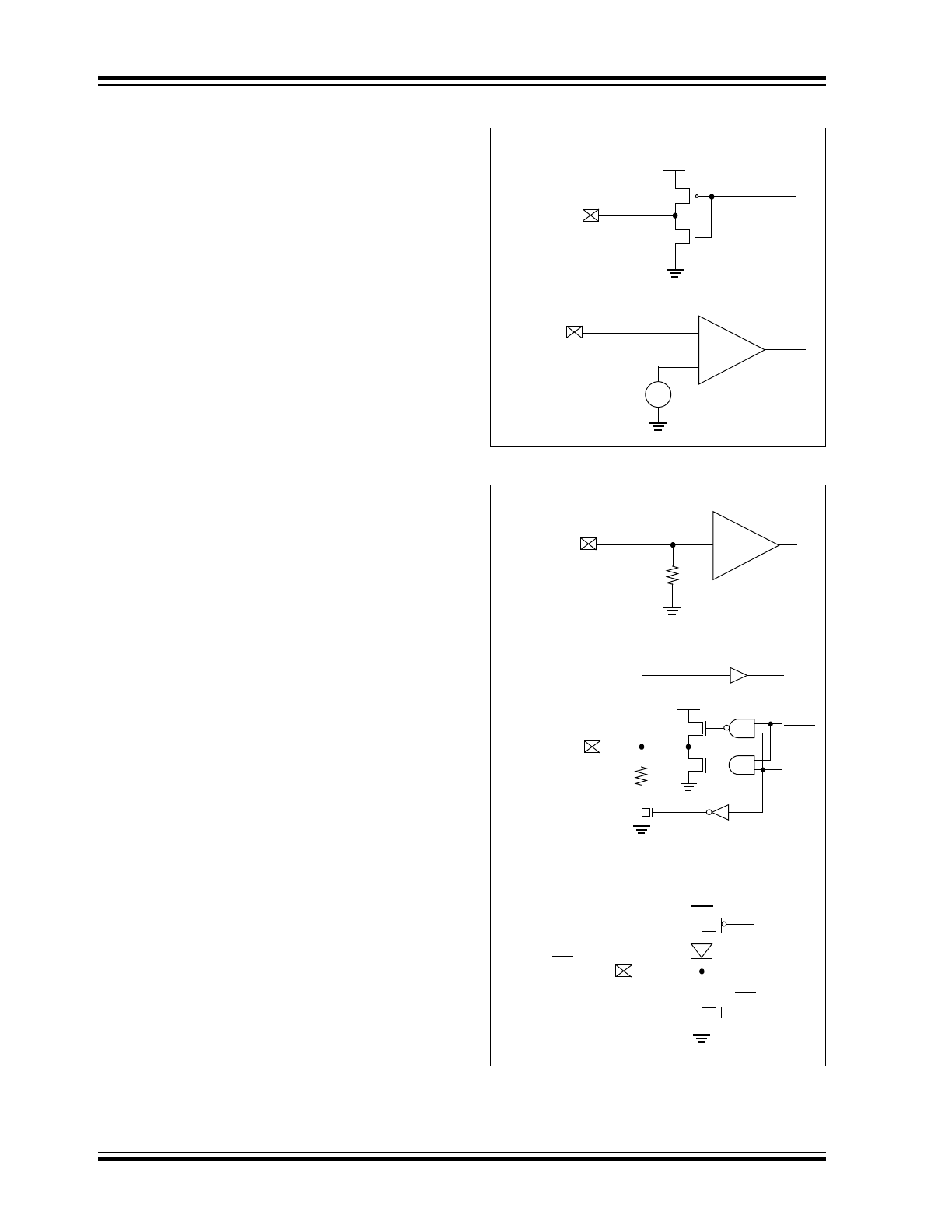
I/O CIRCUITS
FIGURE 2-3:
I/O CIRCUITS (CONTINUED)
DATA, RFEN
N
P
Figure 2-2(D)
STEP
Outputs
V
IN
Figure 2-2(E)
+
-
1.2V
V
DD
S0, S1, S2
Inputs
S3, S4, SHIFT
Z
IN
Figure 2-3(A)
LED Output
LED
Figure 2-3(C)
V
DD
LED
Weak
S5/SLEEP
Z
IN
V
DD
S5
P
N
SOEN
Figure 2-3(B)
N
P
N
SLEEP
2011 Microchip Technology Inc.
DS41111E-page 7
HCS370
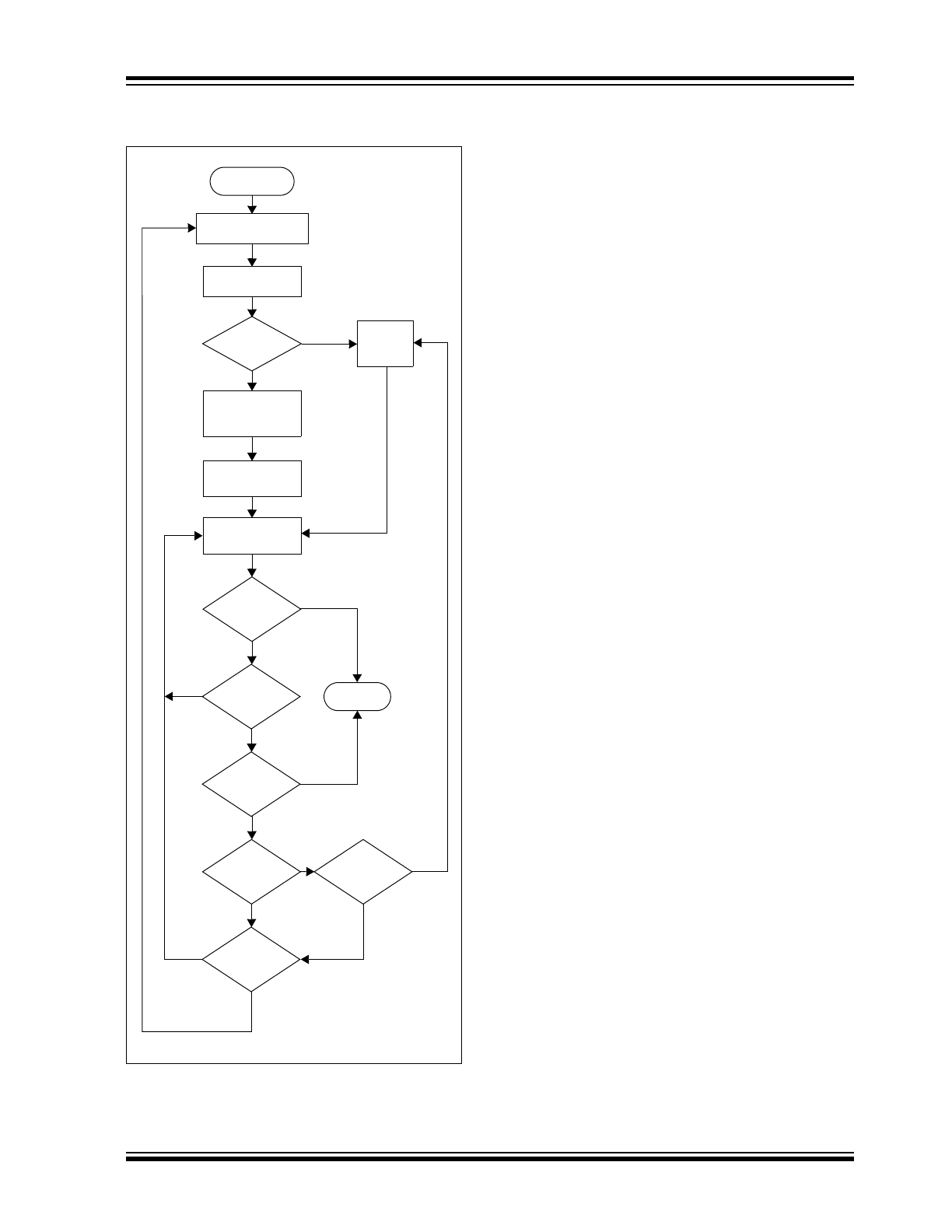
FIGURE 2-4:
BASIC FLOW DIAGRAM OF
THE DEVICE OPERATION
START
Sample Buttons
Increment
Seed
Time
Out
Encrypt
No
No
Yes
Get Config
TX?
Counter
Transmit
MTX
No
Buttons
Seed
Time
Read
Seed
STOP
Yes
Yes
No
Yes
No
No
Yes
Yes
Yes
Seed
Button
No
New
Buttons
No
HCS370
DS41111E-page 8
2011 Microchip Technology Inc.
3.0
EEPROM ORGANIZATION
A summary of the HCS370 EEPROM organization is
shown in the three tables below. The address column
shows the starting address of the option, and its length
or bit position. Options larger than 8 bits are stored
with the Most Significant bits at the given address.
Enough consecutive 8-bit blocks are reserved for the
entire option size. Options such as SEED1, which
have a length that is not an exact multiple of 8 bits, is
stored right justified in the reserved space. Additional
smaller options such as SDBT1 may be stored in the
same address as the Most Significant bits.
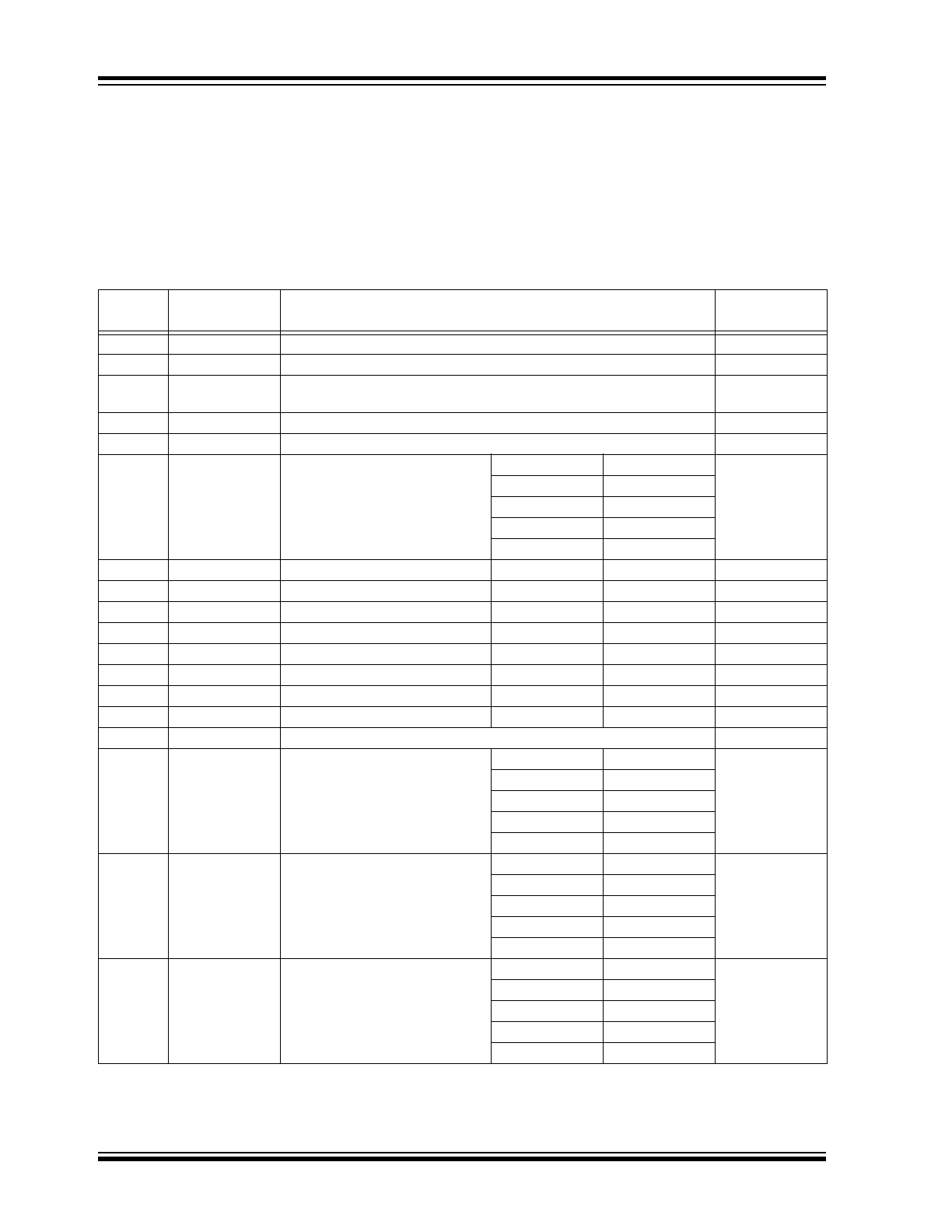
TABLE 3-1:
ENCODER1 OPTIONS (SHIFT = 0)
Symbol
Address
16
:Bits
Description
(1)
Reference
Section
KEY1
1E: 64 bits
Encoder Key
3.2.2
SEED1
14: 60 bits
Encoder Seed Value
3.3
SYNC1
00: 20 bits
00: 18 bits
Encoder Synchronization Counter (CNTSEL=1)
Encoder Synchronization Counter (CNTSEL=0) plus overflow
3.2, 3.2.1
SER1
10: 32 bits
Encoder Serial Number
3.2.2
DISC1
1C: 10 bits
Encoder Discrimination value
3.2, 3.2.1
MSEL1
1C: ---- 32--
Transmission Modulation Format
Value
2
Format
4.1
00
PWM
01
Manchester
10
VPWM
11
PPM
HSEL1
1C: ---4 ----
Header Select
4
T
E
= 0
10
T
E
= 1
4.1
XSER1
1C: --5- ----
Extended Serial Number
28 bits = 0
32 bits = 1
3.2
QUEN1
1C: -6-- ----
Queue counter Enable
Disable = 0
Enable = 1
5.6
STEN1
1C: 7--- ----
START/STOP Pulse Enable
Disable = 0
Enable = 1
4.1
LEDBL1
3F: -6-- ----
Low Voltage LED Blink
Never = 0
Once = 1
5.3
LEDOS1
3F: 7--- ----
LED On Time Select
(1)
50 ms = 0
100 ms = 1
5.3
SDLM1
3C: ---- ---0
Limited Seed
Disable = 0
Enable = 1
3.3
SDMD1
3C: ---- --1-
Seed Mode
User = 0
Production = 1
3.3
SDBT1
14: 7654 ----
Seed Button Code
3.3
SDTM1
3C: ---- 32--
Time Before Seed Code Word
(1)
Value
2
Time (s)
3.3
00
0.0
01
0.8
10
1.6
11
3.2
BSEL1
3C: --54 ----
Transmission Baud Rate Select
(1)
Value
2
T
E
(
μ
s)
4.1
00
100
01
200
10
400
11
800
GSEL1
3C: 76-- ----
Guard Time Select
(1)
Value
2
Time (ms)
4.1, 5.2
00
2 T
E
01
6.4
10
51.2
11
102.4
Note 1: All Timing values vary ±10%.
2011 Microchip Technology Inc.
DS41111E-page 9
HCS370
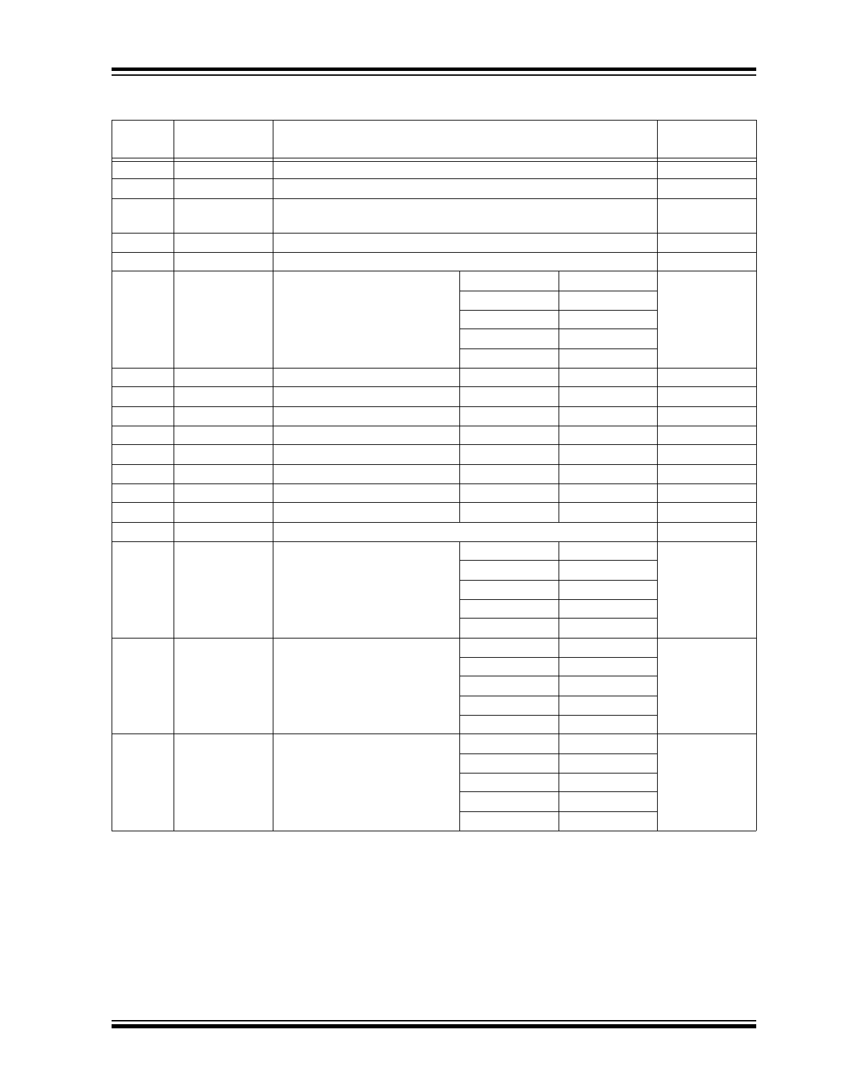
TABLE 3-2:
ENCODER2 OPTIONS (SHIFT = 1)
Symbol
Address
16
:Bits
Description
(1)
Reference
Section
KEY2
34: 64 bits
Encoder Key
3.2.1
SEED2
2A: 60 bits
Encoder Seed Value
3.3
SYNC2
08: 20 bits
08: 18 bits
Encoder Synchronization Counter (CNTSEL=1)
Encoder Synchronization Counter (CNTSEL=0) plus overflow
3.2,
3.2.1
SER2
26: 32 bits
Encoder Serial Number
3.2, 3.2.2
DISC2
32: 10 bits
Encoder Discrimination value
3.2,
3.2.1
MSEL2
32: ---- 32--
Transmission Modulation
Format
Value
2
Format
4.1
00
PWM
01
Manchester
10
VPWM
11
PPM
HSEL2
32: ---4 ----
Header Select
4 T
E
= 0
10 T
E
= 1
4.1
XSER2
32: --5- ----
Extended Serial Number
28 bits = 0
32 bits = 1
3.2
QUEN2
32: -6-- ----
Queue counter Enable
Disable = 0
Enable = 1
5.6
STEN2
32: 7--- ----
START/STOP Pulse Enable
Disable = 0
Enable = 1
4.1
LEDBL2
3D: -6-- ----
Low Voltage LED Blink
Never = 0
Once = 1
5.3
LEDOS2
3D: 7--- ----
LED On Time Select
(1)
50 ms = 0
100 ms = 1
5.3
SDLM2
3E: ---- ---0
Limited Seed
Disable = 0
Enable = 1
3.3
SDMD2
3E: ---- --1-
Seed Mode
User = 0
Production = 1
3.3
SDBT2
2A: 7654 ----
Seed Button Code
3.3
SDTM2
3E: ---- 32--
Time Before Seed Code word
(1)
Value
2
Time (s)
3.3
00
0.0
01
0.8
10
1.6
11
3.2
BSEL2
3E: --54 ----
Transmission Baud Rate
Select
(1)
Value
2
T
E
(
μs)
4.1
00
100
01
200
10
400
11
800
GSEL2
3E: 76-- ----
Guard Time Select
(1)
Value
2
Time (ms)
4.1, 5.2
00
2 T
E
01
6.4
10
51.2
11
102.4
Note 1: All Timing values vary ±10%.

HCS370
DS41111E-page 10
2011 Microchip Technology Inc.
TABLE 3-3:
DEVICE OPTIONS
3.1
Dual Encoder Operation
The HCS370 contains two transmitter configurations
with separate serial numbers, encoder keys, discrimi-
nation values, syncronization counters, and seed val-
ues. The code word is calculated using one of two
possible encoder configurations. Most options for code
word and modulation formats can be different from
Encoder 1 and Encoder 2. However, LED and RF
transmitter options have to be the same. The SHIFT
input pin is used to select between the encoder config-
urations. A low on the SHIFT pin will select Encoder 1
and a high will select Encoder 2.
Symbol
Address
16
:Bits
Description
(1)
Reference
Section
WAKE
3F: ---- --10
Wake-up
(1)
Value
2
Value
4.1
00
No Wake-up
01
75 ms 50%
10
50 ms 33.3%
11
100 ms 16.7%
CNTSEL
3F: ---- -2--
Counter Select
16 bits = 0
20 bits = 1
3.2.1
VLOWL
3F: ---- 3---
Low Voltage Latch Enable
Disable = 0
Enable = 1
3.2.3.1
VLOWSEL
3F: ---4 ----
Low Voltage Trip Point Select
(2)
2.2 V = 0
3.2V = 1
3.2.3.1
PLLSEL
3F: --5- ----
PLL Interface Select
ASK = 0
FSK = 1
5.2
MTX
3D: ---- --10
Minimum Code Words
Value
2
Value
2.0
00
1
01
2
10
4
11
8
SOEN
3D: ---- 3---
SLEEP Output Enable
Disable = 0
Enable = 1
5.4
WAIT
3D: ---- -2--
Wait for Step-Up Regulator
Disable = 0
Enable = 1
5.2, 5.4
TSEL
3D: --54 ----
Time-out Select
(1)
Value
2
Time(s)
2.0
00
0.8
01
3.2
10
12.8
11
25.6
Note 1: All Timing values vary ±10%.
2: Voltage thresholds are ±150 mV.