
© 2011 Microchip Technology Inc.
DS40189E-page 1
HCS362
FEATURES
Security
• Programmable 28/32-bit serial number
• Two programmable 64-bit encryption keys
• Programmable 60-bit seed
• Each transmission is unique
• 69-bit transmission code length
• 32-bit hopping code
• 37-bit fixed code (28/32-bit serial number,
4/0-bit function code, 1-bit status, 2-bit CRC/time,
2-bit queue)
• Encryption keys are read protected
Operation
• 2.0V – 6.3V operation
• Four button inputs
• 15 functions available
• Selectable baud rates and code word blanking
• Programmable minimum code word completion
• Battery low signal transmitted to receiver with
programmable threshold
• Non-volatile synchronization data
• PWM and Manchester modulation
Other
• RF Enable output – PLL interface
• Easy to use programming interface
• On-chip EEPROM
• On-chip tunable oscillator and timing components
• Button inputs have internal pull-down resistors
• Current limiting on LED output
• Minimum component count
Enhanced Features Over HCS300
• 60-bit seed vs. 32-bit seed
• 2-bit CRC for error detection
• 28/32-bit serial number select
• Tunable oscillator (
+/ −10% over specified voltage
ranges
)
• Time bits option
• Queue bits
• TSSOP package
• Programmable Time-out and Guard Time
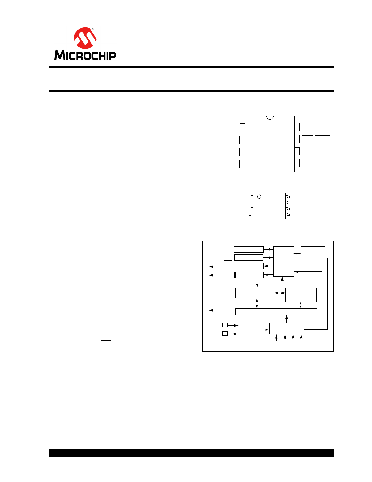
PACKAGE TYPES
HCS362 BLOCK DIAGRAM
Typical Applications
The HCS362 is ideal for Remote Keyless Entry (RKE)
applications. These applications include:
• Automotive RKE systems
• Automotive alarm systems
• Automotive immobilizers
• Gate and garage door openers
• Identity tokens
• Burglar alarm systems
1
2
3
4
8
7
6
5
S0
S1
S2
S3/RFEN
V
DD
LED/SHIFT
DATA
V
SS
PDIP, SOIC
HCS36
2
HCS36
2
S2
S3/RFEN
V
SS
DATA
1
2
3
4
8
7
6
5
S1
S0
V
DD
LED/SHIFT
TSSOP
V
SS
V
DD
Oscillator
RESET Circuit
LED Driver
Controller
Power
Latching
and
Switching
Button Input Port
32-bit Shift Register
Encoder
EEPROM
DATA
LED
S3 S2 S1 S0
SHIFT
PLL Driver
RFEN
K
EE
L
OQ
®
Code Hopping Encoder

HCS362
DS40189E-page 2
© 2011 Microchip Technology Inc.
GENERAL DESCRIPTION
The HCS362 is a code hopping encoder designed for
secure Remote Keyless Entry (RKE) systems. The
HCS362 utilizes the K
EE
L
OQ
®
code hopping technol-
ogy, which incorporates high security, a small package
outline and low cost, to make this device a perfect
solution for unidirectional remote keyless entry sys-
tems and access control systems.
The HCS362 combines a 32-bit hopping code
generated by a nonlinear encryption algorithm, with a
28/32-bit serial number and 9/5 status bits to create a
69-bit transmission stream. The length of the transmis-
sion eliminates the threat of code scanning. The code
hopping mechanism makes each transmission unique,
thus rendering code capture and resend (code grab-
bing) schemes useless.
The crypt key, serial number and configuration data are
stored in an EEPROM array which is not accessible via
any external connection. The EEPROM data is pro-
grammable but read protected. The data can be veri-
fied only after an automatic erase and programming
operation. This protects against attempts to gain
access to keys or manipulate synchronization values.
The HCS362 provides an easy to use serial interface
for programming the necessary keys, system parame-
ters and configuration data.
1.0
SYSTEM OVERVIEW
Key Terms
The following is a list of key terms used throughout this
data sheet. For additional information on K
EE
L
OQ
and
Code Hopping, refer to Technical Brief 3 (TB003).
• RKE - Remote Keyless Entry
• Button Status - Indicates what button input(s)
activated the transmission. Encompasses the 4
button status bits S3, S2, S1 and S0 (Figure 3-2).
• Code Hopping - A method by which a code,
viewed externally to the system, appears to
change unpredictably each time it is transmitted.
• Code word - A block of data that is repeatedly
transmitted upon button activation (Figure 3-2).
• Transmission - A data stream consisting of
repeating code words (Figure 8-1).
• Crypt key - A unique and secret 64-bit number
used to encrypt and decrypt data. In a symmetri-
cal block cipher such as the K
EE
L
OQ
algorithm,
the encryption and decryption keys are equal and
will therefore be referred to generally as the crypt
key.
• Encoder - A device that generates and encodes
data.
• Encryption Algorithm - A recipe whereby data is
scrambled using a crypt key. The data can only be
interpreted by the respective decryption algorithm
using the same crypt key.
• Decoder - A device that decodes data received
from an encoder.
• Decryption algorithm - A recipe whereby data
scrambled by an encryption algorithm can be
unscrambled using the same crypt key.
• Learn – Learning involves the receiver calculating
the transmitter’s appropriate crypt key, decrypting
the received hopping code and storing the serial
number, synchronization counter value and crypt
key in EEPROM. The K
EE
L
OQ
product family facil-
itates several learning strategies to be imple-
mented on the decoder. The following are
examples of what can be done.
- Simple Learning
The receiver uses a fixed crypt key, common
to all components of all systems by the same
manufacturer, to decrypt the received code
word’s encrypted portion.
- Normal Learning
The receiver uses information transmitted
during normal operation to derive the crypt
key and decrypt the received code word’s
encrypted portion.
- Secure Learn
The transmitter is activated through a special
button combination to transmit a stored 60-bit
seed value used to generate the transmitter’s
crypt key. The receiver uses this seed value
to derive the same crypt key and decrypt the
received code word’s encrypted portion.
• Manufacturer’s code – A unique and secret 64-
bit number used to generate unique encoder crypt
keys. Each encoder is programmed with a crypt
key that is a function of the manufacturer’s code.
Each decoder is programmed with the manufac-
turer code itself.
The HCS362 code hopping encoder is designed specif-
ically for keyless entry systems; primarily vehicles and
home garage door openers. The encoder portion of a
keyless entry system is integrated into a transmitter,
carried by the user and operated to gain access to a
vehicle or restricted area. The HCS362 is meant to be
a cost-effective yet secure solution to such systems,
requiring very few external components (Figure 2-1).
Most low-end keyless entry transmitters are given a
fixed identification code that is transmitted every time a
button is pushed. The number of unique identification
codes in a low-end system is usually a relatively small
number. These shortcomings provide an opportunity
for a sophisticated thief to create a device that ‘grabs’
a transmission and retransmits it later, or a device that
quickly ‘scans’ all possible identification codes until the
correct one is found.
The HCS362, on the other hand, employs the K
EE
L
OQ
code hopping technology coupled with a transmission
length of 66 bits to virtually eliminate the use of code
‘grabbing’ or code ‘scanning’. The high security level of
© 2011 Microchip Technology Inc.
DS40189E-page 3
HCS362
the HCS362 is based on the patented K
EE
L
OQ
technol-
ogy. A block cipher based on a block length of 32 bits
and a key length of 64 bits is used. The algorithm
obscures the information in such a way that even if the
transmission information (before coding) differs by only
one bit from that of the previous transmission, the next
coded transmission will be completely different. Statis-
tically, if only one bit in the 32-bit string of information
changes, greater than 50 percent of the coded trans-
mission bits will change.
As indicated in the block diagram on page one, the
HCS362 has a small EEPROM array which must be
loaded with several parameters before use; most often
programmed by the manufacturer at the time of produc-
tion. The most important of these are:
• A 28-bit serial number, typically unique for every
encoder
• A crypt key
• An initial 16-bit synchronization value
• A 16-bit configuration value
The crypt key generation typically inputs the transmitter
serial number and 64-bit manufacturer’s code into the
key generation algorithm (Figure 1-1). The manufac-
turer’s code is chosen by the system manufacturer and
must be carefully controlled as it is a pivotal part of the
overall system security.
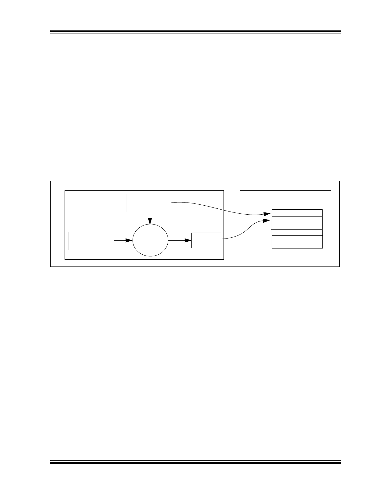
FIGURE 1-1:
CREATION AND STORAGE OF CRYPT KEY DURING PRODUCTION
The 16-bit synchronization counter is the basis behind
the transmitted code word changing for each transmis-
sion; it increments each time a button is pressed. Due
to the code hopping algorithm’s complexity, each incre-
ment of the synchronization value results in greater
than 50% of the bits changing in the transmitted code
word.
Figure 1-2 shows how the key values in EEPROM are
used in the encoder. Once the encoder detects a button
press, it reads the button inputs and updates the syn-
chronization counter. The synchronization counter and
crypt key are input to the encryption algorithm and the
output is 32 bits of encrypted information. This data will
change with every button press, its value appearing
externally to ‘randomly hop around’, hence it is referred
to as the hopping portion of the code word. The 32-bit
hopping code is combined with the button information
and serial number to form the code word transmitted to
the receiver. The code word format is explained in
greater detail in Section 3.1.
A receiver may use any type of controller as a decoder,
but it is typically a microcontroller with compatible firm-
ware that allows the decoder to operate in conjunction
with an HCS362 based transmitter. Section 6.0
provides detail on integrating the HCS362 into a sys-
tem.
A transmitter must first be ‘learned’ by the receiver
before its use is allowed in the system. Learning
includes calculating the transmitter’s appropriate crypt
key, decrypting the received hopping code and storing
the serial number, synchronization counter value and
crypt key in EEPROM.
In normal operation, each received message of valid
format is evaluated. The serial number is used to deter-
mine if it is from a learned transmitter. If from a learned
transmitter, the message is decrypted and the synchro-
nization counter is verified. Finally, the button status is
checked to see what operation is requested. Figure 1-3
shows the relationship between some of the values
stored by the receiver and the values received from
the transmitter.
Transmitter
Manufacturer’s
Serial Number
Code
Crypt
Key
Key
Generation
Algorithm
Serial Number
Crypt Key
Sync Counter
.
.
.
HCS362
Production
Programmer
EEPROM Array
HCS362
DS40189E-page 4
© 2011 Microchip Technology Inc.
FIGURE 1-2:
BUILDING THE TRANSMITTED CODE WORD (ENCODER)
FIGURE 1-3:
BASIC OPERATION OF RECEIVER (DECODER)
NOTE: Circled numbers indicate the order of execution.
Button Press
Information
EEPROM Array
32 Bits
Encrypted Data
Serial Number
Transmitted Information
Crypt Key
Sync Counter
Serial Number
K
EE
L
OQ®
Encryption
Algorithm
Button Press
Information
EEPROM Array
Manufacturer Code
32 Bits of
Encrypted Data
Serial Number
Received Information
Decrypted
Synchronization
Counter
Check for
Match
Sync Counter
Serial Number
K
EE
L
OQ®
Decryption
Algorithm
1
3
4
Check for
Match
2
Perform Function
Indicated by
button press
5
Crypt Key
© 2011 Microchip Technology Inc.
DS40189E-page 5
HCS362
2.0
DEVICE DESCRIPTION
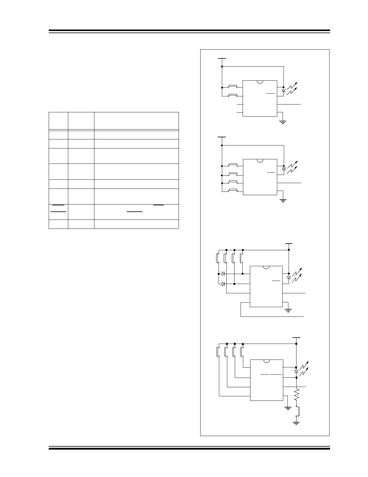
As shown in the typical application circuits (Figure 2-1),
the HCS362 is a simple device to use. It requires only
the addition of buttons and RF circuitry for use as the
transmitter in your security application. See Table 2-1
for a description of each pin and Figure 2-1 for typical
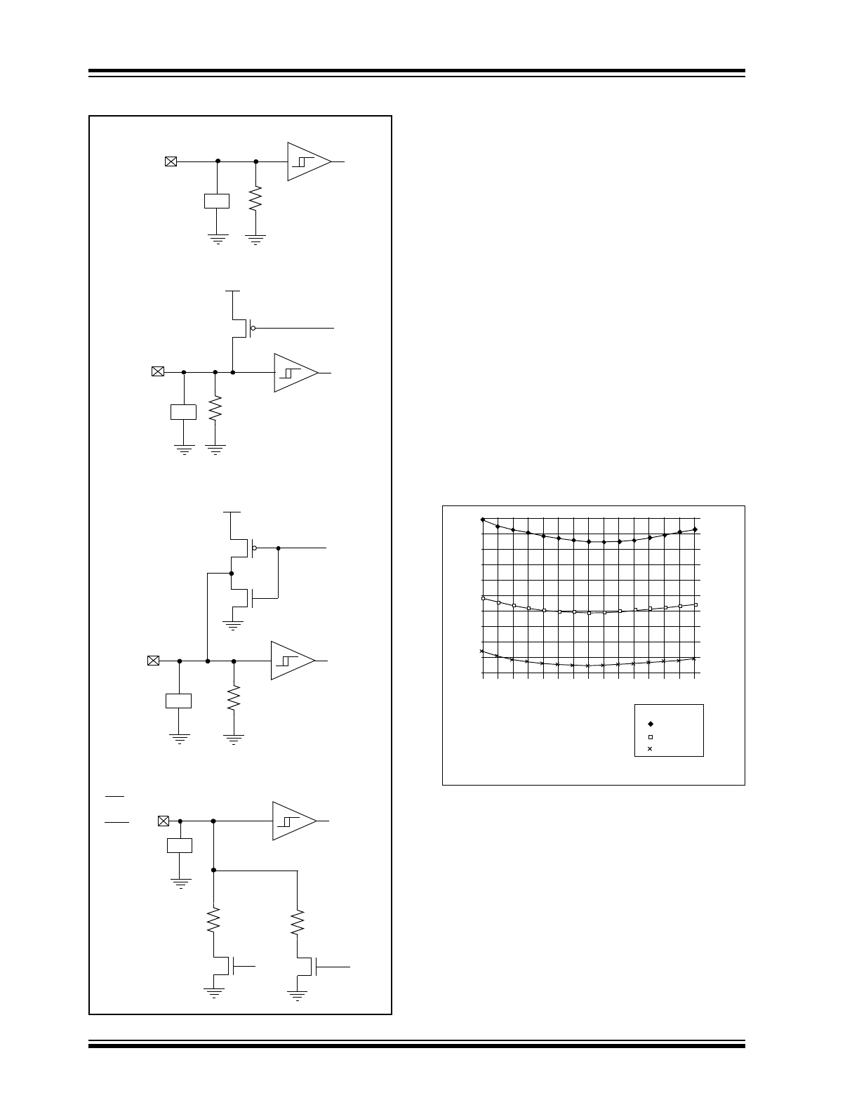
circuits. Figure 2-2 shows the device I/O circuits.
TABLE 2-1:
PIN DESCRIPTIONS
FIGURE 2-1:
TYPICAL CIRCUITS
Name
Pin
Number
Description
S0
1
Switch input 0
S1
2
Switch input 1
S2
3
Switch input 2 / Clock pin when in
Programming mode
S3/
RFEN
4
Switch input 3 / RF enable output
V
SS
5
Ground reference connection
DATA
6
Data output pin / DATA I/O pin for
Programming mode
LED/
SHIFT
7
Cathode connection for LED and
DUAL mode SHIFT input
V
DD
8
Positive supply voltage
V
DD
B0
Tx out
S0
S1
S2
S3
LED
V
DD
DATA
V
SS
a) Two button remote control
B1
V
DD
Tx out
S0
S1
S2
RFEN
V
DD
DATA
V
SS
c) Four button remote control with RF Enable
B3 B2 B1 B0
Note:
Up to 15 functions can be implemented by
pressing more than one button simultane-
ously or by using a suitable diode array.
V
DD
B0
Tx out
S0
S1
S2
S3
V
DD
DATA
V
SS
b) Four button remote control
B1
with PLL output (Note)
PLL control
B2
V
DD
Tx out
S0
S1
S2
S3
V
DD
DATA
V
SS
d) DUAL key, four buttons remote control
B3 B2 B1 B0
SHIFT
1 KW
LED
LED
LED/SHIFT
B3
HCS362
DS40189E-page 6
© 2011 Microchip Technology Inc.
FIGURE 2-2:
I/O CIRCUITS
2.1
Architectural Overview
2.1.1
ONBOARD EEPROM
The HCS362 has an onboard non-volatile EEPROM,
which is used to store user programmable data. The
data can be programmed at the time of production and
include the security-related information such as
encoder keys, serial numbers, discrimination and seed
values. All the security related options are read
protected. The HCS362 has built in protection against
counter corruption. Before every EEPROM write, the
internal circuitry also ensures that the high voltage
required to write to the EEPROM is at an acceptable
level.
2.1.2
INTERNAL RC OSCILLATOR
The HCS362 has an onboard RC oscillator that con-
trols all the logic output timing characteristics. The
oscillator frequency varies within ±10% of the nominal
value (once calibrated over a voltage range of 2V –
3.5V or 3.5V – 6.3V). All the timing values specified in
this document are subject to the oscillator variation.
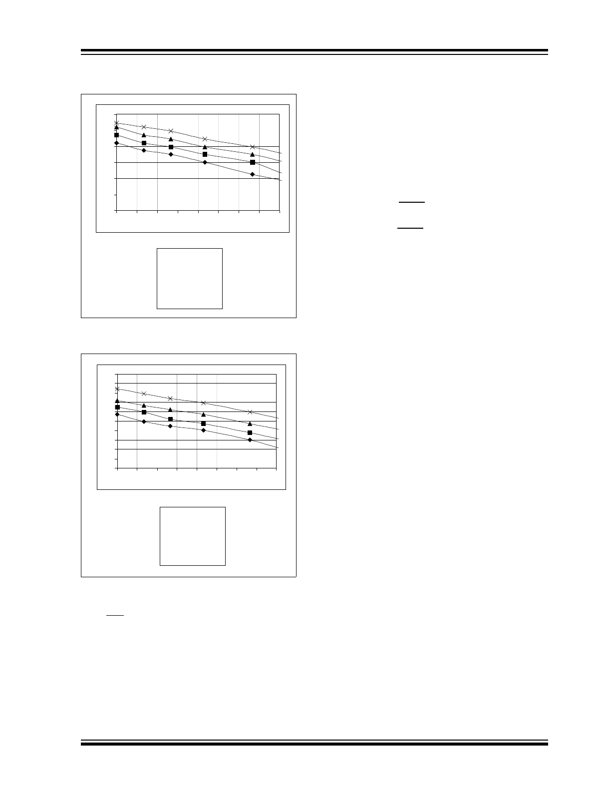
FIGURE 2-3:
HCS362 NORMALIZED T
E
VS.
TEMPERATURE
2.1.3
LOW VOLTAGE DETECTOR
A low battery voltage detector onboard the HCS362
can indicate when the operating voltage drops below a
predetermined value. There are eight options available
depending on the
VLOW
[
0..2
] configuration options.
The options provided are:
S0, S1, S2
ESD
RS
Inputs
V
DD
RFEN
S3 Input/
RS
RDATA
DATA I/O
LED output
RL
RH
V
DD
DATA
LEDH
LEDL
RFEN Output
PFET
NFET
PFET
ESD
ESD
NFET
NFET
ESD
SHIFT input
SHIFT
000
- 2.0V
100
- 4.0V
001
- 2.1V
101
- 4.2V
010
- 2.2V
110
- 4.4V
011
- 2.3V
111
- 4.6V
0.94
1.10
1.08
1.06
1.04
1.02
1.00
0.98
0.96
0.92
0.90
T
E
V
DD
Legend
= 2.0V
= 3.0V
= 6.0V
Typical
T
E
Temperature °C
-50-40-30-20-10 0 10 20 30 40 50 6070 80 90
Note:
Values are for calibrated oscillator
T
E
© 2011 Microchip Technology Inc.
DS40189E-page 7
HCS362
FIGURE 2-4:
HCS362 V
LOW
DETECTOR
(TYPICAL)
FIGURE 2-5:
HCS362 V
LOW
DETECTOR
(TYPICAL)
The output of the low voltage detector is transmitted in
each code word, so the decoder can give an indication
to the user that the transmitter battery is low. Operation
of the LED changes as well to further indicate that the
battery is low and needs replacing.
2.2
Dual Encoder Operation
The HCS362 contains two crypt keys (possibly derived
from two different Manufacturer’s Codes), but only one
Serial Number, one set of Discrimination bits, one 16-
bit Synchronization Counter and a single 60-bit Seed
value. For this reason the HCS362 can be used as an
encoder in multiple (two) applications as far as they
share the same configuration: transmission format,
baud rate, header and guard settings. The SHIFT input
pin (multiplexed with the LED output) is used to select
between the two crypt keys.
A logic 1 on the SHIFT input pin selects the first crypt
key.
A logic 0 on the SHIFT input pin will select the second
crypt key.
1.5
1.7
1.9
2.1
2.3
2.5
2.7
-40
-25
-10
5
20
35
50
65
80
V
DD
(V
)
Temperature (°C)
V
DD
Legend
◆
= 000
■
= 001
▲
= 010
✖
= 011
V
DD
(V)
Temperature (°C)
3.5
3.7
3.9
4.1
4.3
4.5
4.7
4.9
5.1
5.3
5.5
-40
-25
-10
5
20
35
50
65
80
V
DD
Legend
◆
= 000
■
= 001
▲
= 010
✖
= 011
HCS362
DS40189E-page 8
© 2011 Microchip Technology Inc.
3.0
DEVICE OPERATION
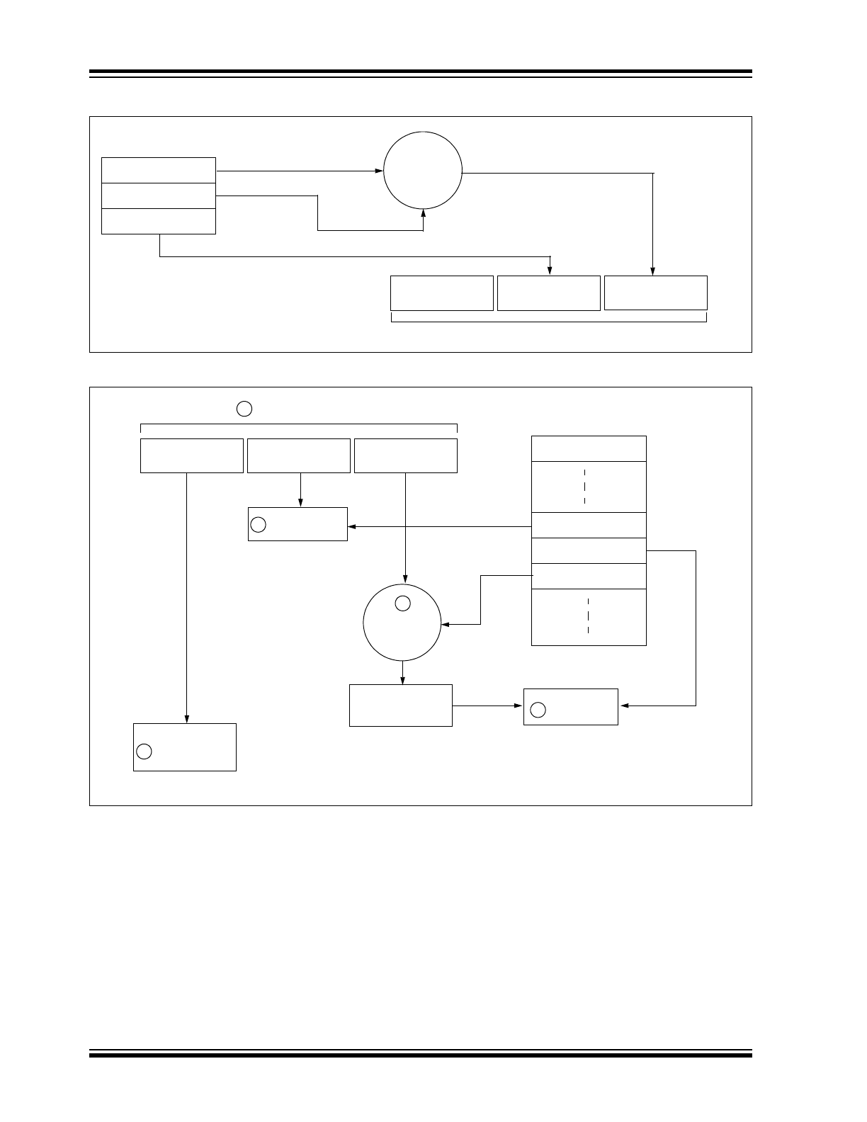
The HCS362 will wake-up upon detecting a switch clo-
sure and then delay for switch debounce (Figure 3-1).
The synchronization information, fixed information and
switch information will be encrypted to form the hop-
ping code. The encrypted or hopping code portion of
the transmission will change every time a button is
pressed, even if the same button is pushed again.
Keeping a button pressed for a long time will result in
the same code word being transmitted until the button
is released or time-out occurs.
The time-out time can be selected with the Time-out
(
TIMOUT
[
0..1
]) configuration option. This option
allows the time-out to be disabled or set to 0.8 s, 3.2 s
or 25.6 s. When a time-out occurs, the device will go
into SLEEP mode to protect the battery from draining
when a button gets stuck.
If in the transmit process, it is detected that a new but-
ton is pressed, the current code word will be aborted. A
new code word will be transmitted and the time-out
counter will RESET. If all the buttons are released, the
minimum code words will be completed. The minimum
code words can be set to 1,2,4 or 8 using the Minimum
Code Words (
MTX
[
0..1
]) configuration option. If the
time for transmitting the minimum code words is longer
than the time-out time, the device will not complete the
minimum code words.
A code that has been transmitted will not occur again
for more than 64K transmissions. This will provide
more than 18 years of typical use before a code is
repeated based on 10 operations per day. Overflow
information programmed into the encoder can be used
by the decoder to extend the number of unique trans-
missions to more than 192K.
FIGURE 3-1:
BASIC FLOW DIAGRAM OF
THE DEVICE OPERATION
Note:
Buttons removed will not have any
effect on the code word unless no but-
tons remain pressed in which case the
current code word will be completed
and the power-down will occur.
START
Sample Buttons
Increment
Seed
Time-out
Encrypt
No
No
Yes
Get Config.
TX?
Counter
Transmit
MTX
No
Buttons
Seed
Time
Read
Seed
STOP
Yes
Yes
No
Yes
No
No
Yes
Yes
Yes
Seed
Button
No
New
Buttons
No
No
© 2011 Microchip Technology Inc.
DS40189E-page 9
HCS362
3.1
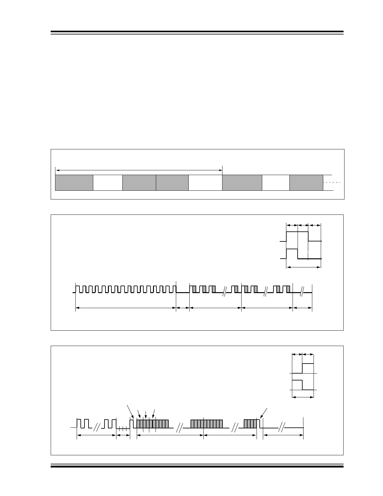
Transmission Modulation Format
The HCS362 transmission is made up of several code
words. Each code word starts with a preamble and a
header, followed by the data (see Figure 3-1 and
Figure 3-2).
The code words are separated by a Guard Time that
can be set to 0 ms, 6.4 ms, 25.6 ms or 76.8 ms with the
Guard Time Select (
GUARD
[
0..1
]) configuration
option. All other timing specifications for the modulation
formats are based on a basic timing element (T
E
). This
Timing Element can be set to 100
μs, 200 μs, 400 μs
or 800
μs with the Baud Rate Select (
BSEL
[
0..1
])
configuration option. The Header Time can be set to
3 T
E
or 10 T
E
with the Header Select (HEADER) Con-
figuration option.
There are two different modulation formats available on
the HCS362 that can be set according to the Modula-
tion Select (MOD) configuration option:
• Pulse Width Modulation (PWM)
• Manchester Encoding
The various formats are shown in Figure 3-3 and
Figure 3-4.
FIGURE 3-2:
CODE WORD TRANSMISSION SEQUENCE
FIGURE 3-3:
TRANSMISSION FORMAT (PWM)
FIGURE 3-4:
TRANSMISSION FORMAT (MANCHESTER)
Header
Encrypt
Fixed
Guard
1 CODE WORD
Preamble
Encrypt
Preamble
Header
LOGIC "1"
Guard
Time
31 T
E
Encrypted
Portion
Fixed Code
Portion
LOGIC "0"
Preamble
3-10
Header
T
E
T
E
T
E
T
E
1
16
T
BP
Guard
Preamble
Header
Encrypted
Fixed Code
1 2
START bit
STOP bit
Time
Portion
Portion
16
bit 0 bit 1 bit 2
LOGIC "0"
LOGIC "1"
T
E
T
E
T
BP

HCS362
DS40189E-page 10
© 2011 Microchip Technology Inc.
3.1.1
CODE HOPPING DATA
The hopping portion is calculated by encrypting the
counter, discrimination value and function code with the
Encoder Key (KEY). The counter is a 16-bit counter.
The discrimination value is 10 bits long and there are 2
counter overflow bits (OVR) that are cleared when the
counter wraps to 0. The rest of the 32 bits are made up
of the function code also known as the button inputs.
3.1.2
FIXED CODE DATA
The 32 bits of fixed code consist of 28 bits of the serial
number (SER) and another copy of the function code.
This can be changed to contain the whole 32-bit serial
number with the Extended Serial Number (XSER) con-
figuration option.
3.1.3
STATUS INFORMATION
The status bits will always contain the output of the Low
Voltage detector (V
LOW
), the Cyclic Redundancy
Check (CRC) bits (or TIME bits depending on CTSEL)
and the Button Queue information.
3.1.3.1
Low Voltage Detector Status (V
LOW
)
The output of the low voltage detector is transmitted
with each code word. If V
DD
drops below the selected
voltage, a logic ‘
1
’ will be transmitted. The output of the
detector is sampled before each code word is transmit-
ted.
3.1.3.2
Button Queue Information (QUEUE)
The queue bits indicate a button combination was
pressed again within 2 s after releasing the previous
activation. Queuing or repeated pressing of the same
buttons (or button combination) is detected by the
HCS362 button debouncing circuitry.
The Queue bits are added as the last two bits of the
standard code word. The queue bits are a 2-bit counter
that does not wrap. The counter value starts at ‘
00b’
and is incremented, if a button is pushed within 2 s of
the previous button press. The current code word is ter-
minated when the buttons are queued. This allows
additional functionality for repeated button presses.
The button inputs are sampled every 6.4 ms during this
2 s period.
00
- first activation
01
- second activation
10
- third activation
11
- from fourth activation on
3.1.3.3
Cyclic Redundancy Check (CRC)
The CRC bits are calculated on the 65 previously trans-
mitted bits. The decoder can use the CRC bits to check
the data integrity before processing starts. The CRC
can detect all single bit errors and 66% of double bit
errors. The CRC is computed as follows:
EQUATION 3-1:
CRC Calculation
and
with
and Di
n
the nth transmission bit 0
≤ n ≤ 64
Note:
The CRC may be wrong when the bat-
tery voltage is around either of the
V
LOW
trip points. This may happen
because V
LOW
is sampled twice each
transmission, once for the CRC calcu-
lation (PWM is LOW) and once when
V
LOW
is transmitted (PWM is HIGH).
V
DD
tends to move slightly during a
transmission which could lead to a dif-
ferent value for V
LOW
being used for
the CRC calculation and the transmis-
sion.
Work around: If the CRC is incorrect,
recalculate for the opposite value of
V
LOW
.
CRC 1
[ ]
n
1
+
CRC 0
[ ]
n
Di
n
⊕
=
CRC 0
[ ]
n
1
+
CRC 0
[ ]
n
Di
n
⊕
(
)
CRC 1
[ ]
n
⊕
=
CRC 1 0
,
[
]
0
0
=