
© 2011 Microchip Technology Inc.
DS40146F-page 1
FEATURES
Security
• Programmable 28/32-bit serial number
• Programmable 64-bit encryption key
• Each transmission is unique
• 67-bit transmission code length
• 32-bit hopping code
• 35-bit fixed code (28/32-bit serial number,
4/0-bit function code, 1-bit status, 2-bit CRC)
• Encryption keys are read protected
Operating
• 2.0-6.6V operation
• Four button inputs
- 15 functions available
• Selectable baud rate
• Automatic code word completion
• Battery low signal transmitted to receiver
• Nonvolatile synchronization data
• PWM and VPWM modulation
Other
• Easy to use programming interface
• On-chip EEPROM
• On-chip oscillator and timing components
• Button inputs have internal pull-down resistors
• Current limiting on LED output
• Minimum component count
Enhanced Features Over HCS300
• 48-bit seed vs. 32-bit seed
• 2-bit CRC for error detection
• 28/32-bit serial number select
• Two seed transmission methods
• PWM and VPWM modulation
• Wake-up signal in VPWM mode
• IR Modulation mode
Typical Applications
The HCS361 is ideal for Remote Keyless Entry (RKE)
applications. These applications include:
• Automotive RKE systems
• Automotive alarm systems
• Automotive immobilizers
• Gate and garage door openers
• Identity tokens
• Burglar alarm systems
DESCRIPTION
The HCS361 is a code hopping encoder designed for
secure Remote Keyless Entry (RKE) systems. The
HCS361 utilizes the K
EE
L
OQ®
code hopping technol-
ogy, which incorporates high security, a small package
outline and low cost, to make this device a perfect
solution for unidirectional remote keyless entry sys-
tems and access control systems.
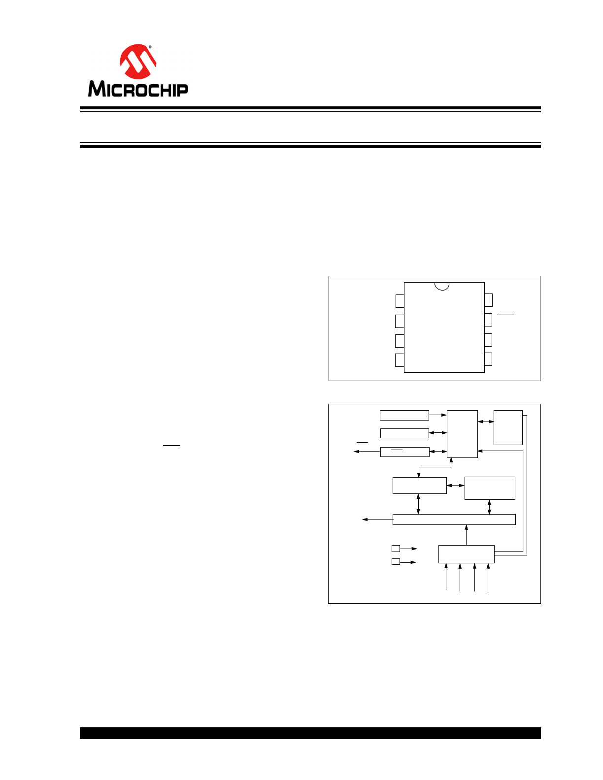
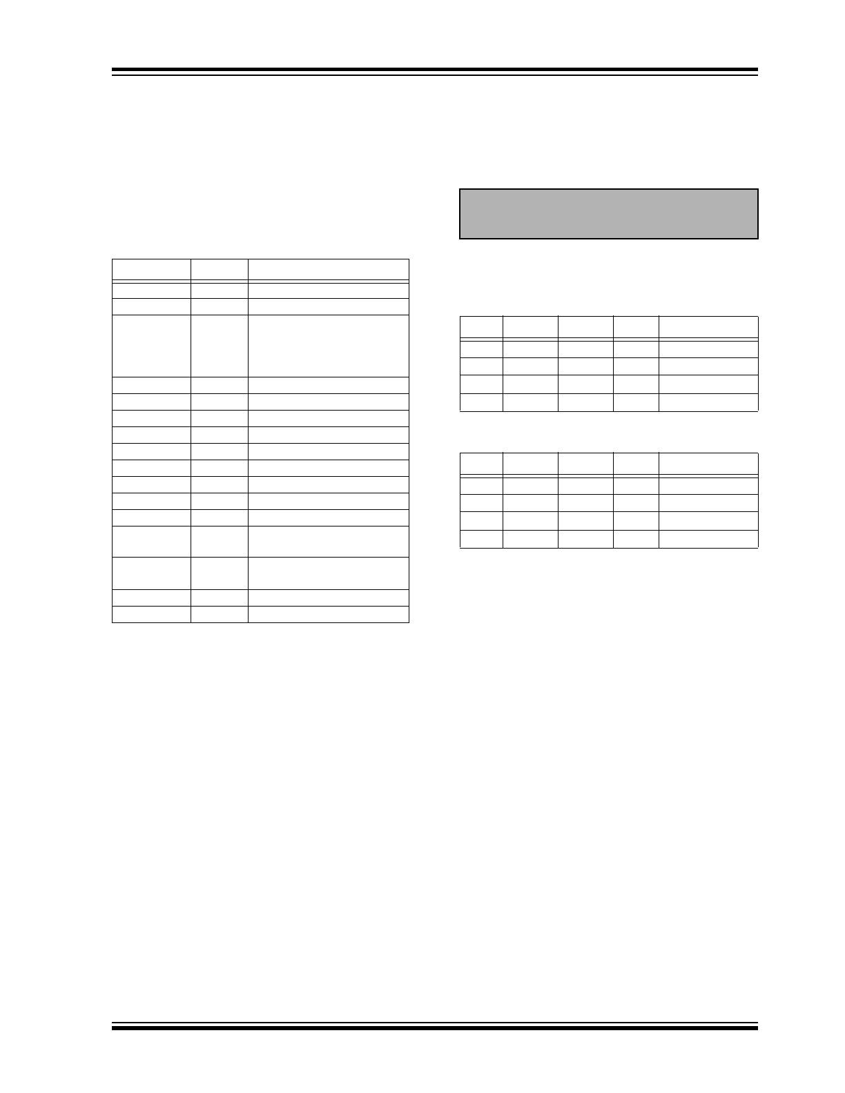
PACKAGE TYPES
HCS361 BLOCK DIAGRAM
DESCRIPTION
The HCS361 combines a 32-bit hopping code
generated by a nonlinear encryption algorithm, with a
28/32-bit serial number and 7/3 status bits to create a
67-bit transmission stream.
1
2
3
4
8
7
6
5
S0
S1
S2
S3
V
DD
LED
DATA
V
SS
PDIP, SOIC
HCS361
V
SS
V
DD
Oscillator
RESET circuit
LED driver
Controller
Power
latching
and
switching
Button input port
32-bit shift register
Encoder
EEPROM
DATA
LED
S
3
S
2
S
1
S
0
HCS361
K
EE
L
OQ®
Code Hopping Encoder

HCS361
DS40146F-page 2
© 2011 Microchip Technology Inc.
The crypt key, serial number and configuration data are
stored in an EEPROM array which is not accessible via
any external connection. The EEPROM data is pro-
grammable but read protected. The data can be veri-
fied only after an automatic erase and programming
operation. This protects against attempts to gain
access to keys or manipulate synchronization values.
The HCS361 provides an easy-to-use serial interface
for programming the necessary keys, system parame-
ters and configuration data.
1.0
SYSTEM OVERVIEW
Key Terms
The following is a list of key terms used throughout this
data sheet. For additional information on K
EE
L
OQ
and
Code Hopping, refer to Technical Brief 3 (TB003).
• RKE - Remote Keyless Entry
• Button Status - Indicates what button input(s)
activated the transmission. Encompasses the 4
button status bits S3, S2, S1 and S0 (Figure 3-2).
• Code Hopping - A method by which a code,
viewed externally to the system, appears to
change unpredictably each time it is transmitted.
• Code word - A block of data that is repeatedly
transmitted upon button activation (Figure 3-2).
• Transmission - A data stream consisting of
repeating code words (Figure 9-1).
• Crypt key - A unique and secret 64-bit number
used to encrypt and decrypt data. In a symmetri-
cal block cipher such as the K
EE
L
OQ
algorithm,
the encryption and decryption keys are equal and
will therefore be referred to generally as the crypt
key.
• Encoder - A device that generates and encodes
data.
• Encryption Algorithm - A recipe whereby data is
scrambled using a crypt key. The data can only be
interpreted by the respective decryption algorithm
using the same crypt key.
• Decoder - A device that decodes data received
from an encoder.
• Decryption algorithm - A recipe whereby data
scrambled by an encryption algorithm can be
unscrambled using the same crypt key.
• Learn –
Learning involves the receiver calculating
the transmitter’s appropriate crypt key, decrypting
the received hopping code and storing the serial
number, synchronization counter value and crypt
key in EEPROM. The K
EE
L
OQ
product family facil-
itates several learning strategies to be imple-
mented on the decoder. The following are
examples of what can be done.
- Simple Learning
The receiver uses a fixed crypt key, common
to all components of all systems by the same
manufacturer, to decrypt the received code
word’s encrypted portion.
- Normal Learning
The receiver uses information transmitted
during normal operation to derive the crypt
key and decrypt the received code word’s
encrypted portion.
- Secure Learn
The transmitter is activated through a special
button combination to transmit a stored 60-bit
seed value used to generate the transmitter’s
crypt key. The receiver uses this seed value
to derive the same crypt key and decrypt the
received code word’s encrypted portion.
• Manufacturer’s code – A unique and secret 64-
bit number used to generate unique encoder crypt
keys. Each encoder is programmed with a crypt
key that is a function of the manufacturer’s code.
Each decoder is programmed with the manufac-
turer code itself.
The HCS361 code hopping encoder is designed specif-
ically for keyless entry systems; primarily vehicles and
home garage door openers. The encoder portion of a
keyless entry system is integrated into a transmitter,
carried by the user and operated to gain access to a
vehicle or restricted area. The HCS361 is meant to be
a cost-effective yet secure solution to such systems,
requiring very few external components (Figure 2-1).
Most low-end keyless entry transmitters are given a
fixed identification code that is transmitted every time a
button is pushed. The number of unique identification
codes in a low-end system is usually a relatively small
number. These shortcomings provide an opportunity
for a sophisticated thief to create a device that ‘grabs’
a transmission and retransmits it later, or a device that
quickly ‘scans’ all possible identification codes until the
correct one is found.
The HCS361, on the other hand, employs the K
EE
L
OQ
code hopping technology coupled with a transmission
length of 66 bits to virtually eliminate the use of code
‘grabbing’ or code ‘scanning’. The high security level of
the HCS361 is based on the patented K
EE
L
OQ
technol-
ogy. A block cipher based on a block length of 32 bits
and a key length of 64 bits is used. The algorithm
obscures the information in such a way that even if the
transmission information (before coding) differs by only
one bit from that of the previous transmission, the next
© 2011 Microchip Technology Inc.
DS40146F-page 3
HCS361
coded transmission will be completely different. Statis-
tically, if only one bit in the 32-bit string of information
changes, greater than 50 percent of the coded trans-
mission bits will change.
As indicated in the block diagram on page one, the
HCS361 has a small EEPROM array which must be
loaded with several parameters before use; most often
programmed by the manufacturer at the time of produc-
tion. The most important of these are:
• A 28-bit serial number, typically unique for every
encoder
• A crypt key
• An initial 16-bit synchronization value
• A 16-bit configuration value
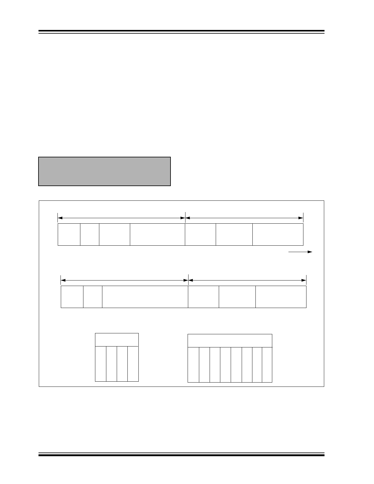
The crypt key generation typically inputs the transmitter
serial number and 64-bit manufacturer’s code into the
key generation algorithm (Figure 1-1). The manufac-
turer’s code is chosen by the system manufacturer and
must be carefully controlled as it is a pivotal part of the
overall system security.
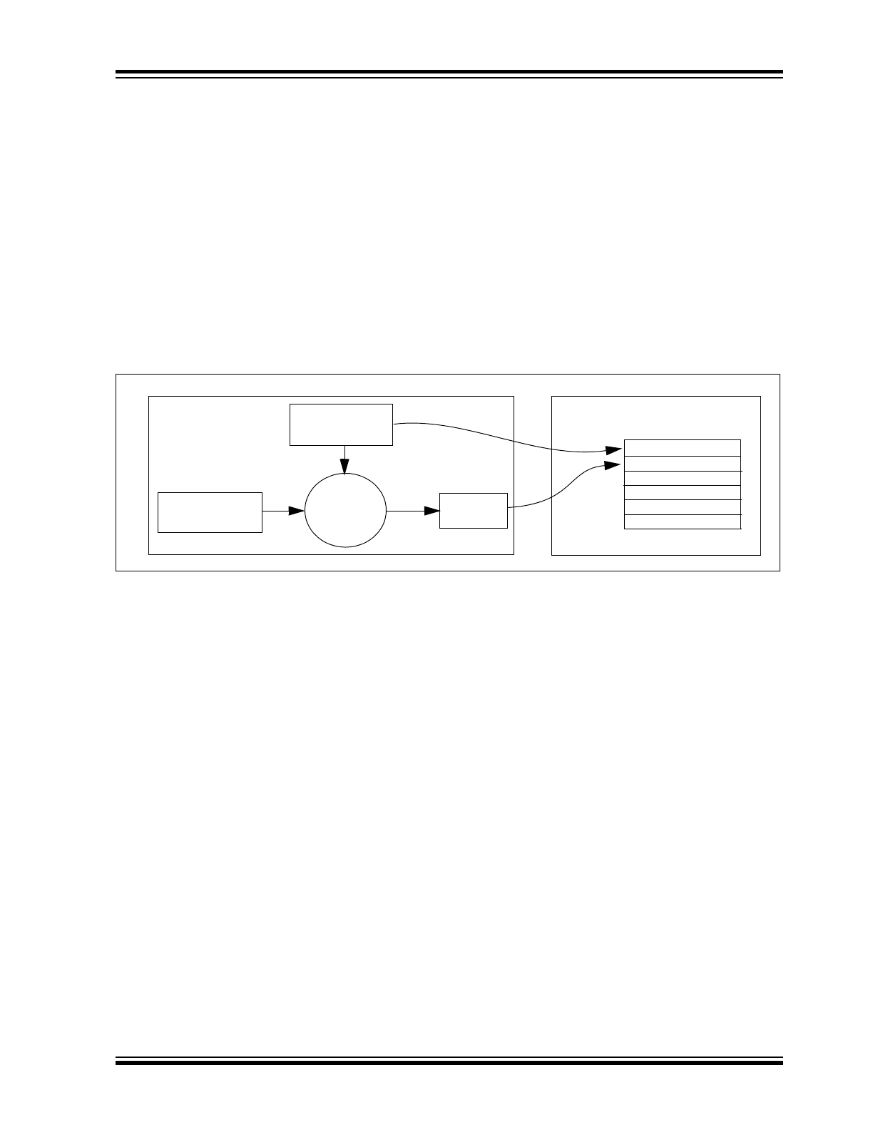
FIGURE 1-1:
CREATION AND STORAGE OF CRYPT KEY DURING PRODUCTION
The 16-bit synchronization counter is the basis behind
the transmitted code word changing for each transmis-
sion; it increments each time a button is pressed. Due
to the code hopping algorithm’s complexity, each incre-
ment of the synchronization value results in greater
than 50% of the bits changing in the transmitted code
word.
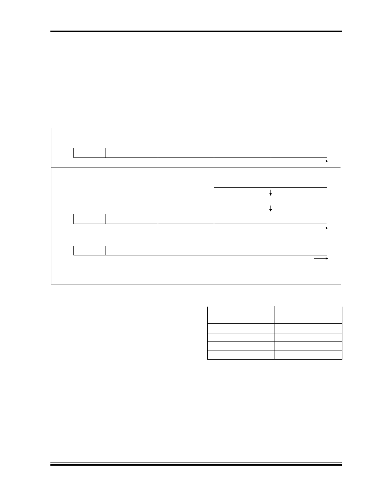
Figure 1-2 shows how the key values in EEPROM are
used in the encoder. Once the encoder detects a button
press, it reads the button inputs and updates the syn-
chronization counter. The synchronization counter and
crypt key are input to the encryption algorithm and the
output is 32 bits of encrypted information. This data will
change with every button press, its value appearing
externally to ‘randomly hop around’, hence it is referred
to as the hopping portion of the code word. The 32-bit
hopping code is combined with the button information
and serial number to form the code word transmitted to
the receiver. The code word format is explained in
greater detail in Section 4.2.
A receiver may use any type of controller as a decoder,
but it is typically a microcontroller with compatible firm-
ware that allows the decoder to operate in conjunction
with an HCS361 based transmitter. Section 7.0
provides detail on integrating the HCS361 into a sys-
tem.
A transmitter must first be ‘learned’ by the receiver
before its use is allowed in the system. Learning
includes calculating the transmitter’s appropriate crypt
key, decrypting the received hopping code and storing
the serial number, synchronization counter value and
crypt key in EEPROM.
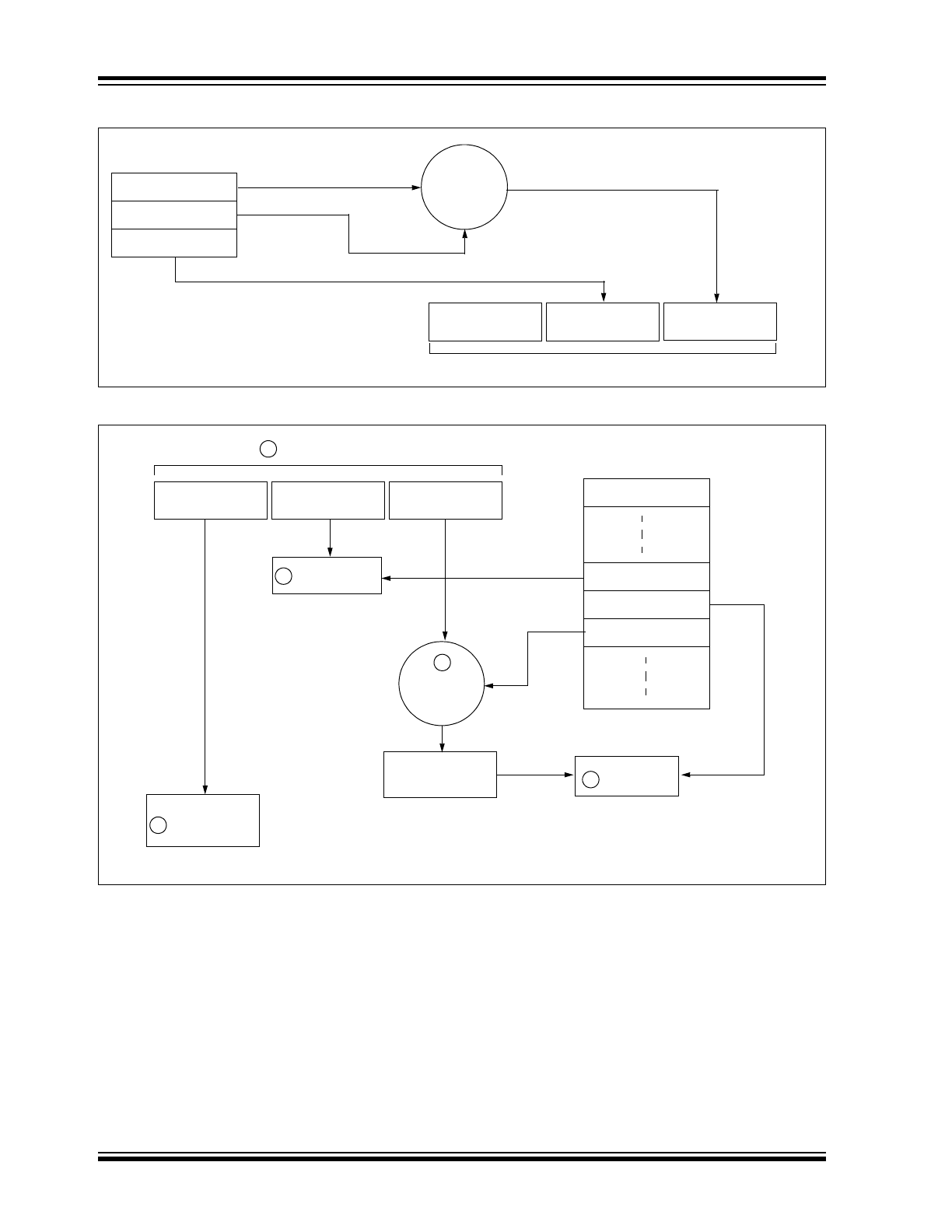
In normal operation, each received message of valid
format is evaluated. The serial number is used to deter-
mine if it is from a learned transmitter. If from a learned
transmitter, the message is decrypted and the synchro-
nization counter is verified. Finally, the button status is
checked to see what operation is requested. Figure 1-3
shows the relationship between some of the values
stored by the receiver and the values received from
the transmitter.
Transmitter
Manufacturer’s
Serial Number
Code
Crypt
Key
Key
Generation
Algorithm
Serial Number
Crypt Key
Sync Counter
.
.
.
HCS361
Production
Programmer
EEPROM Array
HCS361
DS40146F-page 4
© 2011 Microchip Technology Inc.
FIGURE 1-2:
BUILDING THE TRANSMITTED CODE WORD (ENCODER)
FIGURE 1-3:
BASIC OPERATION OF RECEIVER (DECODER)
NOTE: Circled numbers indicate the order of execution.
Button Press
Information
EEPROM Array
32 Bits
Encrypted Data
Serial Number
Transmitted Information
Crypt Key
Sync Counter
Serial Number
K
EE
L
OQ®
Encryption
Algorithm
Button Press
Information
EEPROM Array
Manufacturer Code
32 Bits of
Encrypted Data
Serial Number
Received Information
Decrypted
Synchronization
Counter
Check for
Match
Sync Counter
Serial Number
K
EE
L
OQ®
Decryption
Algorithm
1
3
4
Check for
Match
2
Perform Function
Indicated by
button press
5
Crypt Key
© 2011 Microchip Technology Inc.
DS40146F-page 5
HCS361
2.0
DEVICE OPERATION
As shown in the typical application circuits (Figure 2-1),
the HCS361 is a simple device to use. It requires only
the addition of buttons and RF circuitry for use as the
transmitter in your security application. A description of
each pin is described in Table 2-1.
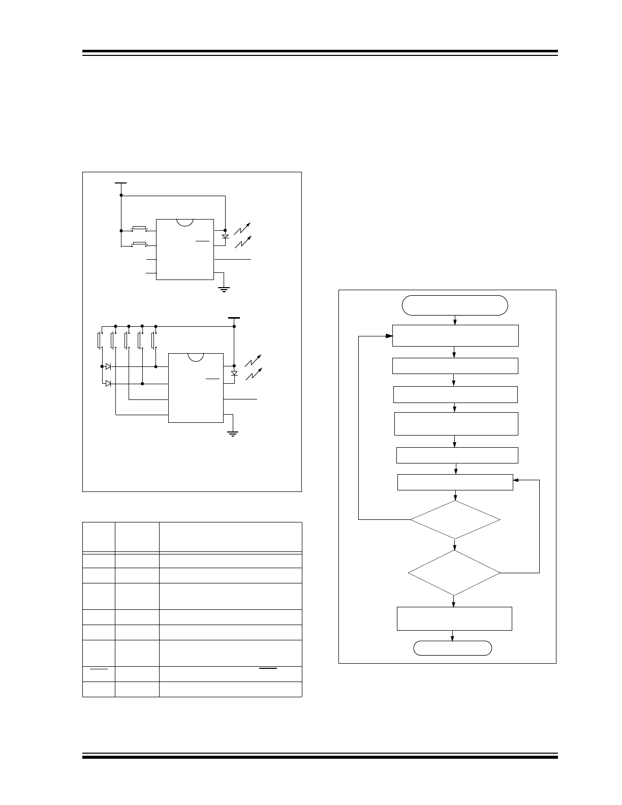
FIGURE 2-1:
Typical circuits
TABLE 2-1:
PIN DESCRIPTIONS
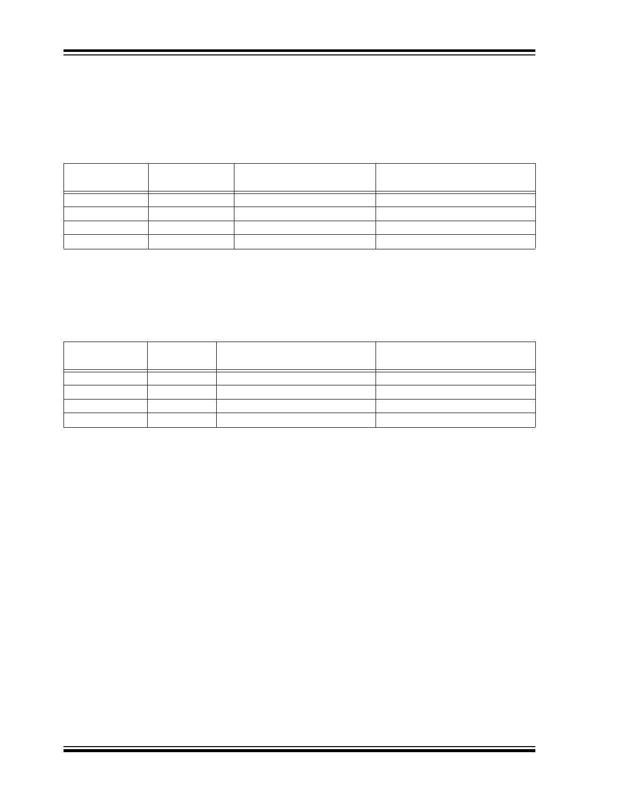
The HCS361 will wake-up upon detecting a button
press and delay approximately 10 ms for button
debounce (Figure 2-2). The synchronization counter,
discrimination value and button information will be
encrypted to form the hopping code. The hopping code
portion will change every transmission, even if the
same button is pushed again. A code word that has
been transmitted will not repeat for more than 64K
transmissions. This provides more than 18 years of use
before a code is repeated; based on 10 operations per
day. Overflow information sent from the encoder can be
used to extend the number of unique transmissions to
more than 192K.
If in the transmit process it is detected that a new but-
ton(s) has been pressed, a RESET will immediately
occur and the current code word will not be completed.
Please note that buttons removed will not have any
effect on the code word unless no buttons remain
pressed; in which case the code word will be completed
and the power-down will occur.
FIGURE 2-2:
ENCODER OPERATION
Name
Pin
Number
Description
S0
1
Switch input 0
S1
2
Switch input 1
S2
3
Switch input 2 / Clock pin when in
Programming mode
S3
4
Switch input 3
V
SS
5
Ground reference
DATA
6
Data output pin /Data I/O pin for
Programming mode
LED
7
Cathode connection for LED
V
DD
8
Positive supply voltage
V
DD
B0
Tx out
S0
S1
S2
S3
LED
V
DD
DATA
V
SS
Two button remote control
B1
V
DD
Tx out
S0
S1
S2
S3
LED
V
DD
DATA
V
SS
Five button remote control (Note
1
)
B4 B3 B2 B1 B0
Note:
Up to 15 functions can be implemented by pressing
more than one button simultaneously or by using a
suitable diode array.
Power-Up
RESET and Debounce Delay
(10 ms)
Sample Inputs
Update Sync Info
Encrypt With
Load Transmit Register
Buttons
Added
?
All
Buttons
Released
?
(A button has been pressed)
Transmit
Stop
No
Yes
No
Yes
Crypt Key
Complete Code
Word Transmission

HCS361
DS40146F-page 6
© 2011 Microchip Technology Inc.
3.0
EEPROM MEMORY
ORGANIZATION
The HCS361 contains 192 bits (12 x 16-bit words) of
EEPROM memory (Table 3-1). This EEPROM array is
used to store the encryption key information,
synchronization value, etc. Further descriptions of the
memory array is given in the following sections.
TABLE 3-1:
EEPROM MEMORY MAP
3.1
KEY_0 - KEY_3 (64-Bit Crypt Key)
The 64-bit crypt key is used to create the encrypted
message transmitted to the receiver. This key is calcu-
lated and programmed during production using a key
generation algorithm. The key generation algorithm
may be different from the K
EE
L
OQ
algorithm. Inputs to
the key generation algorithm are typically the transmit-
ter’s serial number and the 64-bit manufacturer’s code.
While the key generation algorithm supplied from
Microchip is the typical method used, a user may elect
to create their own method of key generation. This may
be done providing that the decoder is programmed with
the same means of creating the key for
decryption purposes.
3.2
SYNC_A, SYNC_B
(Synchronization Counter)
This is the 16-bit synchronization value that is used to
create the hopping code for transmission. This value is
incremented after every transmission. Separate syn-
chronization counters can be used to stay synchro-
nized with different receivers.
3.3
SEED_0, SEED_1, and SEED_2
(Seed Word)
The three word (48 bits) seed code will be transmitted
when seed transmission is selected. This allows the sys-
tem designer to implement the Secure Learn feature or
use this fixed code word as part of a different key genera-
tion/tracking process or purely as a fixed code transmis-
sion.
3.4
SER_0, SER_1
(Encoder Serial Number)
SER_0 and SER_1 are the lower and upper words of
the device serial number, respectively. There are 32
bits allocated for the Serial Number and a selectable
configuration bit determines whether 32 or 28 bits will
be transmitted. The serial number is meant to be
unique for every transmitter.
WORD
ADDRESS
MNEMONIC
DESCRIPTION
0
KEY_0
64-bit crypt key
(word 0) LSb’s
1
KEY_1
64-bit crypt key
(word 1)
2
KEY_2
64-bit crypt key
(word 2)
3
KEY_3
64-bit crypt key
(word 3) MSb’s
4
SYNC_A
16-bit synch counter
5
SYNC_B/
SEED_2
16-bit synch counter B
or Seed value (word 2)
6
RESERVED
Set to 0000H
7
SEED_0
Seed Value
(word 0) LSb’s
8
SEED_1
Seed Value
(word 1) MSb’s
9
SER_0
Device Serial Number
(word 0) LSb’s
10
SER_1
Device Serial Number
(word 1) MSb’s
11
CONFIG
Configuration Word
Note:
Since SEED2 and SYNC_B share the
same memory location, Secure Learn and
Independent mode transmission (including
IR mode) are mutually exclusive.
© 2011 Microchip Technology Inc.
DS40146F-page 7
HCS361
3.5
CONFIG
(Configuration Word)
The Configuration Word is a 16-bit word stored in
EEPROM array that is used by the device to store
information used during the encryption process, as well
as the status of option configurations. Further
explanations of each of the bits are described in the
following sections.
TABLE 3-1:
CONFIGURATION WORD
3.5.1
MOD: MODULATION FORMAT
MOD selects between VPWM modulation and PWM
modulation format.
If MOD = 1, VPWM modulation is selected as well as
the following:
1.
Enables the TXWAK bit to select the WAKE-UP
transmission.
2.
Extends the Guard Time.
If MOD = 0, PWM modulation is selected.
3.5.2
BSEL: BAUD RATE SELECT
BSEL selects the baud rate. If BSEL = 1, the baud rate
is nominally 1667 bits per second and with BSEL = 0,
833 bits per second.
3.5.3
TXWAK: BIT FORMAT SELECT OR
WAKE-UP
In PWM mode, this bit selects the bit format.
If TXWAK = 0, the PWM pulse duty cycle is 1/3-2/3.
If TXWAK = 1, the PWM pulse duty cycle is 1/6-2/6.
In VPWM mode, this bit enables the wake-up signal.
If TXWAK = 0, transmissions start normally with the
preamble portion of the code word.
If TXWAK = 1, transmissions start with a Wake-up
sequence followed by a dead time (see Figure 4-2).
The following tables summarize the combined effect of
TXWAK, BSEL and MOD option bits.
TABLE 3-1:
PWM OPTIONS
TABLE 3-2:
VPWM OPTIONS
3.5.4
SPM: SYNC PULSE MODULATION
Select Modulation mode of Sync Pulse. If SPM = 1, the
sync pulse is modulated (Figure 4-1 and Figure 4-2).
3.5.5
OVR: OVERFLOW
The overflow bit is used to extend the number of possi-
ble synchronization values. The synchronization coun-
ter is 16 bits in length, yielding 65,536 values before the
cycle repeats. Under typical use of 10 operations a day,
this will provide nearly 18 years of use before a
repeated value will be used. Should the system
designer conclude that is not adequate, then the over-
flow bit can be utilized to extend the number of unique
values. This can be done by programming OVR to 1 at
the time of production. The encoder will automatically
clear OVR the first time that the transmitted synchroni-
zation value wraps from 0xFFFF to 0x0000. Once
cleared, OVR cannot be set again, thereby creating a
permanent record of the counter overflow. This pre-
vents fast cycling of 64K counter. If the decoder system
is programmed to track the overflow bits, then the effec-
tive number of unique synchronization values can be
extended to 128K. If programmed to zero, the system
will be compatible with old encoder devices.
Bit Number Symbol
Bit Description
0
BACW
Blank Alternate Code Word
1
BSEL
Baud Rate Selection
2
TXWAK
PWM mode: 1/6, 2/6 or 1/3,
2/3 select
VPWM mode: Wake-up
enable
3
SPM
Sync Pulse Modulation
4
SEED
Seed Transmission enable
5
DELM
Delay mode enable
6
TIMO
Time-out enable
7
IND
Independent mode enable
8 USRA0
User bit
9
USRA1
User bit
10
USRB0
User bit
11
USRB1
User bit
12
XSER
Extended serial number
enable
13
TMPSD
Temporary seed
transmission enable
14
MOD
Modulation format select
15
OVR
Overflow bit
Note:
The Wake-up sequence is transmitted
before the first code word of each trans-
mission only.
MOD TXWAK
BSEL
T
E
Duty Cycle
0
0
0
400us
1/3-2/3
0
0
1
200us
1/3-2/3
0
1
0
200us
1/6-2/6
0
1
1
100us
1/6-2/6
MOD TXWAK
BSEL
T
E
Wake-up
1
0
0
400us
NO
1
0
1
200us
NO
1
1
0
400us
YES
1
1
1
200us
YES
HCS361
DS40146F-page 8
© 2011 Microchip Technology Inc.
3.5.6
BACW: BLANK ALTERNATE CODE
WORD
BACW = 1 selects the encoder to transmit every sec-
ond code word. This can be used to reduce the aver-
age power transmitted over a 100 ms window and
thereby transmit a higher peak power (see
Section 5.2).
3.5.7
XSER: EXTENDED SERIAL
NUMBER
If XSER = 0, the four Most Significant bits of the Serial
Number are substituted by S[3:0] and the code word
format is compatible with the HCS200/300/301.
If XSER = 1, the full 32-bit Serial Number [SER_1,
SER_0] is transmitted.
3.5.8
DISCRIMINATION VALUE
While in other K
EE
L
OQ
encoders its value is user
selectable, the HCS361 uses directly the 8 Least Sig-
nificant bits of the Serial Number as part of the infor-
mation that form the encrypted portion of the
transmission (Figure 3-2).
The discrimination value aids the post-decryption
check on the decoder end. After the receiver has
decrypted a transmission, the discrimination bits are
checked against the encoder Serial Number to verify
that the decryption process was valid.
3.5.9
USRA,B: USER BITS
User bits form part of the discrimination value. The user
bits together with the IND bit can be used to identify the
counter that is used in Independent mode.
FIGURE 3-2:
CODE WORD ORGANIZATION
Note:
Since the button status S[3:0] is used to
detect a Seed transmission, Extended
Serial Number and Secure Learn are
mutually exclusive.
Discrimination Bits
(12 bits)
I
O
U
U
S
S
... S
N V
S
S
E
E
... E
D R
R
R
R
R
... R
1
0
7
6
...
0
Fixed Code Portion of Transmission
Encrypted Portion of Transmission
67 bits
of Data
Transmitted
MSB
LSB
CRC
(2-bit)
V
LOW
(1-bit)
Button
Status
(4 bits)
28-bit
Serial Number
Button
Status
(4 bits)
Discrimination
bits
(12 bits)
16-bit
Sync Value
Button Status
(4 bits)
S
S
S
S
2
1
0
3
Fixed Code Portion of Transmission
Encrypted Portion of Transmission
MSB
LSB
CRC
(2-bit)
V
LOW
(1-bit)
32-bit
Extended Serial Number
Button
Status
(4 bits)
Discrimination
bits
(12 bits)
16-bit
Sync Value
XSER=1
XSER=0
© 2011 Microchip Technology Inc.
DS40146F-page 9
HCS361
3.5.10
SEED: ENABLE SEED
TRANSMISSION
If SEED = 0, seed transmission is disabled. The Inde-
pendent Counter mode can only be used with seed
transmission disabled since SEED_2 is shared with the
second synchronization counter.
With SEED = 1, seed transmission is enabled. The
appropriate button code(s) must be activated to trans-
mit the seed information. In this mode, the seed infor-
mation (SEED_0, SEED_1, and SEED_2) and the
upper 12 or 16 bits of the serial number (SER_1)are
transmitted instead of the hop code.
Seed transmission is available for function codes
(Table 3-2) S[3:0] = 1001 and S[3:0] = 0011 (delayed).
This takes place regardless of the setting of the IND bit.
The two seed transmissions are shown in Figure 3-3.
FIGURE 3-3:
Seed Transmission
3.5.11
TMPSD: TEMPORARY SEED
TRANSMISSION
The temporary seed transmission can be used to dis-
able learning after the transmitter has been used for a
programmable number of operations. This feature can
be used to implement very secure systems. After learn-
ing is disabled, the seed information cannot be
accessed even if physical access to the transmitter is
possible. If TMPSD = 1 the seed transmission will be
disabled after a number of code hopping transmis-
sions. The number of transmissions before seed trans-
mission is disabled, can be programmed by setting the
synchronization counter (SYNC_A or SYNC_B) to a
value as shown in Table 3-4.
TABLE 3-4:
SYNCHRONOUS COUNTER
INITIALIZATION VALUES
All examples shown with XSER = 1, SEED = 1
When S[3:0] = 1001, delay is not applicable.
CRC+V
LOW
SER_1
SEED_2
SEED_1
SEED_0
Data transmission direction
For S[3:0] = 0x3 before delay:
16-bit Data Word
16-bit Counter
Encrypt
CRC+V
LOW
SER_1
SER_0
Encrypted Data
For S[3:0] = 0011 after delay (Note 1, Note 2):
CRC+V
LOW
SER_1
SEED_2
SEED_1
SEED_0
Data transmission direction
Data transmission direction
Note 1: For Seed Transmission, SEED_2 is transmitted instead of SER_0.
2: For Seed Transmission, the setting of DELM has no effect.
Synchronous Counter
Values
Number of
Transmissions
0000H
128
0060H
64
0050H
32
0048H
16
HCS361
DS40146F-page 10
© 2011 Microchip Technology Inc.
3.5.12
DELM: DELAY MODE
If DELM = 1, delay transmission is enabled. A delayed
transmission is indicated by inverting the lower nibble
of the discrimination value. The Delay mode is primarily
for compatibility with previous K
EE
L
OQ
devices.
If DELM = 0, delay transmission is disabled (Table 3-
1).
TABLE 3-1:
TYPICAL DELAY TIMES
3.5.13
TIMO: TIME-OUT
OR AUTO-SHUTOFF
If TIMO = 1, the time-out is enabled. Time-out can be
used to terminate accidental continuous transmissions.
When time-out occurs, the PWM output is set low and
the LED is turned off. Current consumption will be
higher than in Standby mode since current will flow
through the activated input resistors. This state can be
exited only after all inputs are taken low. TIMO = 0, will
enable continuous transmission (Table 3-5).
TABLE 3-5:
TYPICAL TIME-OUT TIMES
TXWAK
BSEL
Number of Code Words before
Delay Mode
Time Before Delay Mode (MOD = 0)
0
0
28
≈ 2.8s
0
1
56
≈ 2.9s
1
0
28
≈ 2.6s
1
1
56
≈ 2.8s
TXWAK
BSEL
Maximum Number of Code Words
Transmitted
Time Before Time-out (MOD = 0)
0
0
256
≈ 25.6s
0
1
512
≈ 27.2s
1
0
256
≈ 23.8s
1
1
512
≈ 25.4s