
R&E International
A Subsidiary of Microchip Technology Inc.
RE46C120
CMOS Ionization Smoke Detector ASIC
Product Specification
General Description
The RE46C120 is a low power CMOS ionization type
smoke detector IC. With a few external components
this circuit will provide all the required features for an
ionization type smoke detector.
An internal oscillator strobes power to the smoke
detection circuitry for 10.5mS every 1.66 seconds to
keep standby current to a minimum. A check for a low
battery condition is performed every 40 seconds when
in standby. The TONE input allows for selection of a
temporal pattern or a 2/3 duty cycle continuous tone.
The temporal horn pattern supports the NFPA 72
emergency evacuation signal.
Although this device was designed for smoke detection
utilizing an ionization chamber it could be used in a
variety of security applications.
© 2009 Microchip Technology Inc.
DS22157B-page 1
The RE46C120 is recognized by Underwriters
Laboratories for use in smoke detectors that comply
with specification UL217 and UL268.
Features
• Guard Outputs for Ion Detector Input
• +/-0.75pA Detect Input Current
• Internal Reverse Battery Protection
• Internal Low Battery Detection
• Pin Selectable Horn Pattern
• Low Quiescent Current Consumption (<6.5uA)
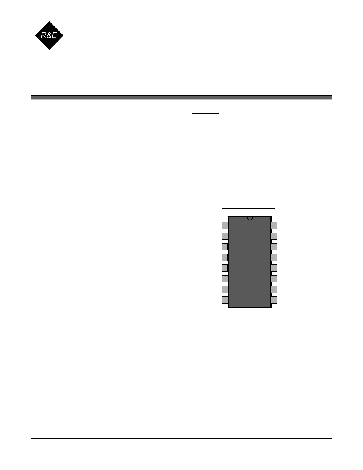
• 16L
PDIP
• ESD Protection on all Pins
• Compatible with MC145017, MC14467
• UL Recognized per File S24036
• Available in RoHS Compliant Pb Free Packaging
Pin Configuration
16
1
DETCOMP
GUARD2
15
2
DETECT
N/C
14
3
GUARD1
LBADJ
13
4
VSEN
TONE
ABSOLUTE MAXIMUM RATINGS
PARAMETER SYMBOL
VALUE
UNITS
Supply Voltage
V
DD
15 V
Input Voltage Range Except FEED
V
in
-.3 to V
dd
+.3 V
FEED Input Voltage Range
V
infd
-10 to +22
V
Reverse Battery Time
T
RB
5 S
Input Current except FEED
I
in
10
MA
Operating Temperature
T
A
-10 to 60
°C
Storage Temperature
T
STG
-55 to 125
°C
Maximum Junction Temperature
T
J
150
°C
Stresses beyond those listed under Absolute Maximum Ratings may cause permanent damage to the device. These are
stress ratings only and operation at these conditions for extended periods may affect device reliability.
This product utilizes CMOS technology with static protection; however proper ESD prevention procedures should be used
when handling this product. Damage can occur when exposed to extremely high static electrical charge
12
5
OSCAP
LED
VDD
RBIAS
FEED
HS
11
6
HB
VSS
8
9
10
7

RE46C120
CMOS Ionization Smoke Detector ASIC R&E International
Product Specification
A Subsidiary of Microchip Technology
Inc.
© 2009 Microchip Technology Inc.
DS22157B-page 2
DC Electrical Characteristics at TA = 25°C, VDD=9V, VSS=0V (unless otherwise noted)
Limits
Parameter Symbol
Test
Pin Test
Conditions Min Typ Max Units
Supply Voltage
V
DD
6
Operating
6 12
V
I
DD1
6
RBIAS=8.2MΩ, OSCAP=.1uF
4.5
6.5
uA
Supply Current
I
DD2
6
RBIAS=8.2MΩ, OSCAP=.1uF;Vdd=12V
9
uA
Input Voltage High
V
IH
4,8
6.2 4.5
V
Input Voltage Low
V
IL
4,8
4.5 2.7 V
IL
DET1
15
VDD=9V, DETECT=VSS, 0-40% RH
-0.75
pA
IL
DET2
15
VDD=9V, DETECT=VSS, 85% RH
Note 1
-1.50
pA
IL
TONE
4
TONE=VSS, RBIAS=8.2MΩ,
-100 -450
nA
Input Leakage Low
IL
FD
8
FEED=-10V
-50
uA
IH
DET1
15
VDD=9V, DETECT=VDD, 0-40% RH
0.75
pA
IH
DET2
15
VDD=9V, DETECT=VDD, 85% RH
Note 1
1.50
pA
Input Leakage High
IH
FD
8
FEED=22V
50
uA
Output Off Leakage High
I
OHZ
5
LED Off
1
uA
V
OH1
10,11
IOH=-16mA, VDD=7.2V
6.3 V
Output Voltage High
V
OH2
1
IOH=-30ua
8.5 V
V
OL1
10,11
IOL=16mA, VDD=7.2V
.9
V
V
OL2
1
IOL=30ua
.5
V
Output Voltage Low
V
OL3
5
IOL=10mA, VDD=7.2V
3
V
Low Battery Voltage
V
LB
6
T
A
=-10 to 60ºC, Note 3
7.2 7.5 7.8 V
V
SET1
13
47 50 53
%V
DD
Internal Sensitivity Set Voltage
V
SET2
3
65.5 %V
DD
VG
OS1
14,15
Guard Amplifier
-50 50
mV
VG
OS2
15,16
Guard Amplifier
-50 50
mV
Offset Voltage
VG
OS3
13,15
Smoke Comparator
-50 50
mV
V
CM1
14,15
Guard Amplifier, Note 2
2
V
DD
-.5 V
Common Mode Voltage
V
CM2
13,15
Smoke Comparator, Note 2
.5
V
DD
-2 V
Output Impedance
Z
OUT
14,16
Guard Amplifier Outputs, Note 2
10
k
Ω
Hysteresis
V
HYS
13
No Alarm to Alarm Condition
90 130 170 mV
Note 1: Sample test only
Note 2: Not 100% production tested
Note 3: Production test at room with temperature guardbanded limits.
RE46C120
CMOS Ionization Smoke Detector ASIC R&E International
Product Specification
A Subsidiary of Microchip Technology
Inc.
AC Electrical Characteristics at TA = 25°C, VDD=9V, OSCAP=.1uF, RBIAS=8.2MΩ, VSS=0V (unless
otherwise noted)
Limits
Parameter Symbol
Test
Pin Test
Conditions Min Typ Max Units
T
PER1
12
No Alarm Condition
1.34 1.67 2
S
Oscillator Period
T
PER2
12
Alarm Condition
37.5 41.5 45.8 mS
Oscillator Pulse Width
T
PW
5
Operating
9.1 10.5 12.9 mS
LED On Time
T
LON
5
Operating
9.1 10.5 12.9 mS
T
LOF1
5
Standby, No Alarm
32 40 48 S
LED Off Time
T
LOF2
5
Alarm Condition
.9 1 1.1 S
T
HON1
10,11
Operating, Alarm Condition, Note 4,
TONE=VDD or Float
450 500 550 mS
T
HON2
10,11
Low Battery, No Alarm
9.1
10.5 12.9 mS
Horn On Time
T
HON3
10,11
Operating, Alarm Condition, TONE=Low
150 166 183 mS
T
HOF1
10,11
Operating, Alarm Condition, Note 4,
TONE=VDD or Float
450 500 550 mS
T
HOF2
10,11
Operating, Alarm Condition, Note 4,
TONE=VDD or Float
1.35 1.5 1.65 S
T
HOF3
10,11
Operating, Alarm Condition, TONE=Low
75 83 92 mS
Horn Off Time
T
HOF4
10,11
Low Battery, No Alarm
32 40 48 S
Note 4: See timing diagram for Horn Temporal Pattern
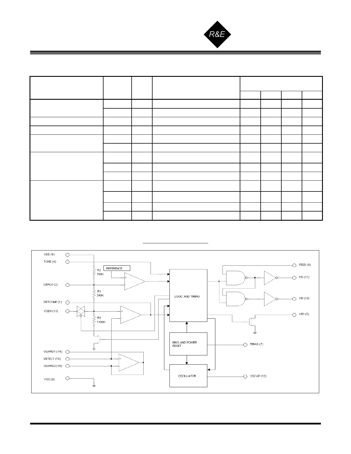
Functional Block Diagram
Figure 1
© 2009 Microchip Technology Inc.
DS22157B-page 3

RE46C120
CMOS Ionization Smoke Detector ASIC R&E International
Product Specification
A Subsidiary of Microchip Technology
Inc.
© 2009 Microchip Technology Inc.
DS22157B-page 4
DEVICE DESCRIPTION and APPLICATION NOTES
Note: All timing references are nominal values. Refer to the electrical specifications for limits
Internal Timing – With external components as indicated on the application drawing the period of the oscillator is
1.67 seconds in standby. Every 1.66 seconds the detection circuitry is powered up for 10.5mS and the status of
the smoke comparator is latched. In addition every 40 seconds the LED driver is turned on for 10.5mS and the
status of the low battery comparator is latched. The smoke comparator status is not checked during the low
battery test, during the low battery horn warning chirp, or when the horn is on due to an alarm condition.
If an alarm condition is detected the oscillator period increases to 41.5mS.
Due to the low currents used in the oscillator the capacitor on pin 12 should be a low leakage type. Oscillator
accuracy will depend mainly on the tolerance of the RBIAS resistor and OSCAP capacitor.
Smoke Detection Circuit – The smoke comparator compares the ionization chamber voltage to a voltage derived
from a resistor divider across VDD. This divider voltage is available externally on pin 13 (VSEN). When smoke is
detected this voltage is internally increased by 130mV nominal to provide hysteresis and make the detector less
sensitive to false triggering.
Pin 13 (VSEN) can be used to modify the internal set point for the smoke comparator by using external resistors
to VDD or VSS. Nominal values for the internal resistor divider are indicated on the block diagram. These internal
resistor values can vary by up to ±20% but the resistor matching will typically be <2% on any one device. A
transmission switch on pin 13 isolates this pin during the low battery test so that the low battery set point will not
be affected if external resistors are used to modify the smoke sensitivity set point.
The guard amplifier and outputs are always active and will be within 50mV of the DETECT input to reduce surface
leakage. The guard outputs also allow for measurement of the DETECT input without loading the ionization
chamber.
Low Battery Detection – An internal Zener reference is compared to the voltage divided VDD supply. The battery
can be checked under load via the LED low side driver output since low battery status is latched at the end of the
10mS LED pulse. Pin 3 (LBADJ) can be used to modify the low battery set point by placing a resistor to VDD or
VSS. Note that the internal resistor string is common to both pin 3 and pin 13 so there will be some interaction
between the two. Modification of the low battery set point may affect the smoke sensitivity setting.
LED Pulse – The LED is pulsed on for 10.5mS every 40S in standby. In alarm the LED is pulsed on for 10.5mS
every 1S.
Testing – At power up all internal registers are reset. By holding pin 12 (OSCAP) low the internal power strobe is
active. Functional testing can be accelerated by driving pin 12 with a 4 kHz square wave however the 10.5mS
strobe period should be maintained for proper operation of the analog circuitry. Please refer to the timing
diagrams.
Horn Tone – Pin 4 selects the NFPA72 horn tone (high or floating) or the 2/3 duty cycle continuous tone (low).
If
this pin is externally connected high, use a current limiting resistor from pin 4 to VDD.
Reverse Battery Protection – The RE46c120 internally limits the current from VSS to VDD in the event of
accidental polarity reversal. If an input is connected to VDD it should be done through a resistance of at least
1.5K to limit the reverse current through this path.
RE46C120
CMOS Ionization Smoke Detector ASIC R&E International
Product Specification
A Subsidiary of Microchip Technology
Inc.
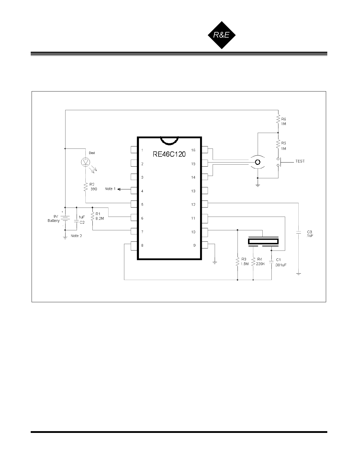
Typical Application
Figure 2
Notes:
1.
Float or connect pin 4 to VDD through 1.5kOhm minimum for NFPA72 temporal horn pattern, connect to VSS for 2/3 duty cycle
continuous tone.
2.
R3, R4 and C1 are typical values and may be adjusted to maximize sound pressure.
3.
C2 should be located as close as possible to the device power pins.
4.
Route the pin 8 PC board trace away from pin 7 to avoid coupling.
© 2009 Microchip Technology Inc.
DS22157B-page 5
RE46C120
CMOS Ionization Smoke Detector ASIC R&E International
Product Specification
A Subsidiary of Microchip Technology
Inc.
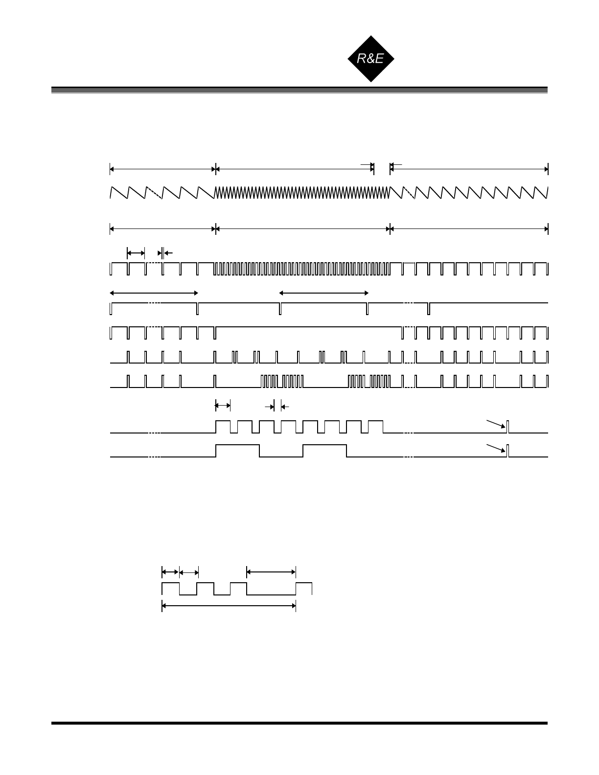
Timing Diagram
Standby Mode; No Low Battery; No Alarm
Alarm; No Low Battery
Alarm; Low Battery
Oscillator
1.67S
10mS
Internal Clock
24 Clock Cycles (40 S)
LED
DETCOMP (pin1)
Sample (2/3 Duty)
Sample (NFPA72)
T
HON3
T
HOF3
Low Battery Warning Chirp
Horn (2/3 Duty Cycle, TONE=VSS)
Low Battery Warning Chirp
Horn (NFPA72, TONE=Open)
See Figure Below for Complete Temporal Horn Cycle
Notes:
1. Smoke is not sampled when the horn is active so the horn cycle is self completing
2. Low battery warning chirp is suppressed in alarm
T
HON1
T
HOF1
Complete Temporal Horn Pattern
Pin 15 > Pin 13
Pin 13 > Pin 15; 130mV Level Shift on Pin 13
No Alarm; Low Battery
T
HOF2
24 Clock Cycles (1S)
Pin 15 > Pin 13
© 2009 Microchip Technology Inc.
DS22157B-page 6

RE46C120
CMOS Ionization Smoke Detector ASIC R&E International
Product Specification
A Subsidiary of Microchip Technology
Inc.
Information contained in this publication regarding device
applications and the like is provided only for your convenience and
may be superseded by updates. It is your responsibility to ensure
that your application meets with your specifications. MICROCHIP
MAKES NO REPRESENTATIONS OR WARRANTIES OF ANY
KIND WHETHER EXPRESS OR IMPLIED, WRITTEN OR ORAL,
STATUTORY OR OTHERWISE, RELATED TO THE
INFORMATION, INCLUDING BUT NOT LIMITED TO ITS
CONDITION, QUALITY, PERFORMANCE, MERCHANTABILITY
OR FITNESS FOR PURPOSE. Microchip disclaims all liability
arising from this information and its use. Use of Microchip devices in
life support and/or safety applications is entirely at the buyer’s risk,
and the buyer agrees to defend, indemnify and hold harmless
Microchip from any and all damages, claims, suits, or expenses
resulting from such use. No licenses are conveyed, implicitly or
otherwise, under any Microchip intellectual property rights.
Trademarks
The Microchip name and logo, the Microchip logo, Accuron,
dsPIC, K
EE
L
OQ
, K
EE
L
OQ
logo,
MPLAB, PIC, PICmicro,
PICSTART, rfPIC, SmartShunt and UNI/O are registered
trademarks of Microchip Technology Incorporated in the U.S.A.
and other countries.
FilterLab, Hampshire, Linear Active Thermistor, MXDEV, MXLAB,
SEEVAL, SmartSensor and The Embedded Control Solutions
Company are registered trademarks of Microchip Technology
Incorporated in the U.S.A.
Analog-for-the-Digital Age, Application Maestro, CodeGuard,
dsPICDEM, dsPICDEM.net, dsPICworks, dsSPEAK, ECAN,
ECONOMONITOR, FanSense, In-Circuit Serial Programming,
ICSP, ICEPIC, Mindi, MiWi, MPASM, MPLAB Certified logo,
MPLIB, MPLINK, mTouch, nanoWatt XLP, PICkit, PICDEM,
PICDEM.net, PICtail, PIC
32
logo, PowerCal, PowerInfo,
PowerMate, PowerTool, REAL ICE, rfLAB, Select Mode, Total
Endurance, TSHARC, WiperLock and ZENA are trademarks of
Microchip Technology Incorporated in the U.S.A. and other
countries.
SQTP is a service mark of Microchip Technology Incorporated in
the U.S.A.
All other trademarks mentioned herein are property of their
respective companies.
© 2009, Microchip Technology Incorporated, Printed in the
U.S.A., All Rights Reserved.
Printed on recycled paper.
Microchip received ISO/TS-16949:2002 certification for its worldwide
headquarters, design and wafer fabrication facilities in Chandler and
Tempe, Arizona; Gresham, Oregon and design centers in California and
India. The Company’s quality system processes and procedures are for its
PIC
®
MCUs and dsPIC
®
DSCs, K
EE
L
OQ
®
code hopping devices, Serial
EEPROMs, microperipherals, nonvolatile memory and analog products. In
addition, Microchip’s quality system for the design and manufacture of
development systems is ISO 9001:2000 certified.
© 2009 Microchip Technology Inc.
DS22157B-page 7