
2002 Microchip Technology Inc.
DS21702A-page 1
M
TC1307
Features
• Four Independent 150 mA LDOs
• Low Supply Current (220 µA typical)
• High Output Voltage Accuracy (0.5% typical)
• Low Dropout Voltage (100 mV typical with
150 mA load)
• Four Independent Shutdown Inputs
• Select Mode
™
: Selectable Output Voltages for
High Design Flexibility
• Integrated Independent Microprocessor Reset
• Low Noise Outputs
• Fast Response from Shutdown (10 µs typical)
• RESET Output for Low Battery Detection or Reset
Generator
• Over Current and Over-Temperature Protection
• Small 16-Pin QSOP Package
• Specified Junction Temperature Range:
- -40°C to +125°C
Applications
• Battery Operated Systems
• Potable Computers
• Set Top Boxes
• Load Partitioning
• Medical Instruments
• Cellular / GSM / PHS Phones
• Instrumentation
• Linear Post Regulator for SMPS
• Pagers
Description
The TC1307 combines four CMOS Low Dropout Linear
Regulators with a Microcontroller Monitor in a space-
saving 16-Pin QSOP package. Developed specifically
for battery powered portable applications, all four out-
puts of the TC1307 typically consume a total of 220 µA
supply current, hold the output voltage to a tolerance of
0.5% and require 100 mV of headroom for regulation at
the maximum output current of 150 mA. In addition to
the four high performance LDOs, the TC1307 also
includes a voltage detector with a delayed RESET out-
put that can be configured for low battery detection or
Microcontroller Reset Generator.
All four LDOs have independent shutdown inputs and
can be programmed using two select inputs making the
TC1307 adaptable for a wide range of multiple output
applications. The tri-state SELECT12 input pin allows
the designer to select the output voltages on V
OUT1
,
and V
OUT2
from three different values (2.5V, 2.8V or
3.0V). The tri-state SELECT34 input pin allows the
designer to select the output voltages on V
OUT3
, and
V
OUT4
from three different values (1.8V, 2.5V or 2.8V).
All four LDO’s require only a 1 µF output capacitor for
stability that can be ceramic, tantalum or aluminum
over the entire input voltage operating range and 0 mA
to 150 mA rated load range. All four LDOs have low
output noise and excellent dynamic response when
faced with sudden line and load changes.
The voltage detect pin is set for a threshold of 2.63V
(typical) and operates down to a minimum input voltage
of 1.0V. When the voltage on the detect pin rises above
the 2.63V threshold, the RESET output is held low for
300 ms (typical).
Additional integrated features include over-current pro-
tection and over-temperature protection providing full
protection from external load faults.
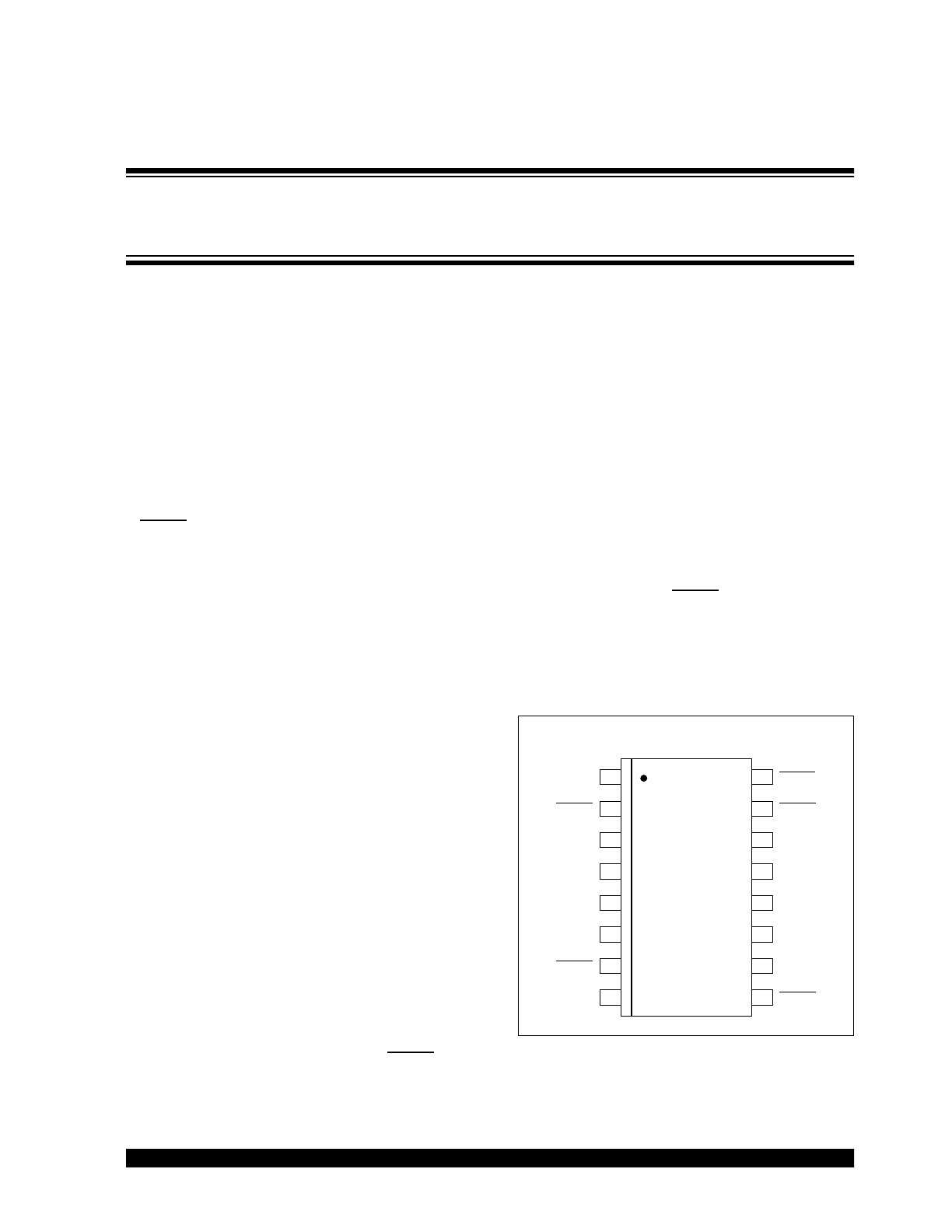
Package Types
TC1307
1
2
3
4
5
6
7
8
9
10
11
12
13
14
15
16
V
DET
SHDN1
SHDN3
SHDN4
SHDN2
SELECT12
SELECT34
V
IN
V
IN
V
IN
RESET
V
OUT
1
V
OUT
2
V
OUT
3
V
OUT
4
GND
QSOP
Four-Channel CMOS LDO with Select Mode, Shutdown and
Independent Reset
TC1307
DS21702A-page 2
2002 Microchip Technology Inc.
1.0
ELECTRICAL
CHARACTERISTICS
1.1
Maximum Ratings*
V
DD
..............................................................................
6.5V
All inputs and outputs w.r.t. ....... ...V
IN
+ 0.3V to -0.3V
Output Short Circuit Current ...... ...............continuous
Storage temperature.................... .... -65°C to +150°C
Operating Junction Temperature,
T
J
..................................................-40°C < T
J
< +150°C
Maximum Junction Temperature, T
J
..................150°C
ESD protection on all pins...................................
≥
4 kV
*Notice: Stresses above those listed under “Maximum
Ratings” may cause permanent damage to the device.
This is a stress rating only and functional operation of
the device at those or any other conditions above those
indicated in the operational listings of this specification
is not implied. Exposure to maximum rating conditions
for extended periods may affect device reliability.
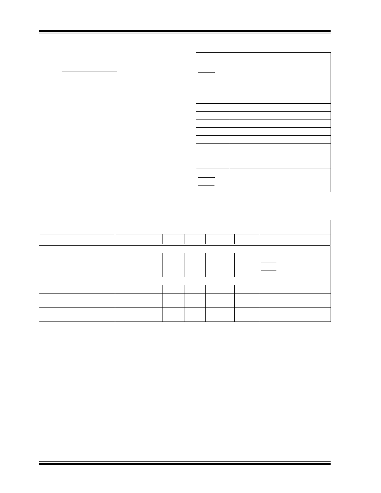
PIN FUNCTION TABLE
ELECTRICAL CHARACTERISTICS
Name
Function
V
DET
Voltage Detect Input
SHDN1
Shutdown for V
OUT1
SELECT12
Input for setting V
OUT1
and V
OUT2.
V
IN
Input Voltage Connection
V
IN
Input Voltage Connection
GND
Ground connection
SHDN3
Shutdown for V
OUT3
V
IN
Input Voltage Connection
SHDN4
Shutdown for V
OUT4
SELECT34
Input for setting V
OUT3
and V
OUT4.
V
OUT4
LDO4 Output
V
OUT3
LDO3 Output
V
OUT2
LDO2 Output
V
OUT1
LDO1 Output
SHDN2
Shutdown for V
OUT2
RESET
Reset Output
Unless otherwise specified, all limits are established for V
IN
= V
R
+1, I
L
= 100 µA, C
L
= 3.3 µF, SHDN > V
IH
, T
A
= 25°C.
Boldface type specifications apply for junction temperatures, T
J
(Note 9) of -40°C to +125°C.
Parameter
Sym
Min
Typ
Max
Units
Conditions
Input Characteristics:
Input Operating Voltage
V
IN
2.7
—
6.0
V
Note 1
Input Quiescent Current
I
IN
—
220
370
µA
SHDN = V
IH
, I
L
= 0
Input Shutdown Current
I
IN_SHDN
—
0.1
0.5
µA
SHDN = 0V
Output Characteristics:
Maximum Output Current
I
OUT_MAX
150
—
mA
Output Short Circuit Current
(Average)
I
OUT_SC
—
360
—
mA
V
OUT
= 0V
Voltage Regulation
LDO1/LDO2/LDO3/LDO4
V
OUT
V
R
-2.5% V
R
±0.5
V
R
+2.5%
V
Note 2
Note 1: The minimum V
IN
must meet two conditions: V
IN
≥
2.7V and V
IN
≥
(V
R
+ 2.5%) + V
DROPOUT
.
2: V
R
is the nominal regulator output voltage. For example: V
R
= 1.8V, 2.5V, 2.8V or 3.0V.
3: TCV
OUT
= (V
OUT-HIGH
- V
OUT-LOW
) * 10
6
/ (V
R
*
∆
Temperature), V
OUT-HIGH
= Highest voltage measured over the tempera-
ture range. V
OUT-LOW
= Lowest voltage measured over the temperature range.
4: Load regulation is measured at a constant junction temperature using low duty cycle pulse testing. Load regulation is
tested over a load range from 1mA to the maximum specified output current. Changes in output voltage due to heating
effects are determined using thermal regulation specification TCV
OUT
.
5: Thermal regulation is defined as the change in output voltage at a time t after a change in power dissipation is applied.
Specifications are for a current pulse equal to I
LMAX
at V
IN
= 6.0V for t = 10 msec.
6: Dropout voltage is defined as the input to output differential at which the output voltage drops 2% below its nominal value
with a 1V differential applied.
7: The maximum allowable power dissipation is a function of ambient temperature, the maximum allowable junction temper-
ature and the thermal resistance from junction to air. (i.e. T
A
, T
J
,
θ
JA
). Exceeding the maximum allowable power dissipa-
tion will cause the device operating junction temperature to exceed the maximum 150°C rating. Sustained junction
temperatures above 150°C can impact the device reliability.
8: V
TH-MIN
= 2.55V and V
TH-MAX
= 2.70V.
9: The Junction temperature is approximated by soaking the device under test at an ambient temperature equal to the
desired Junction temperature. The test time is small enough such that the rise in the Junction temperature over the Ambi-
ent temperature is not significant.
2002 Microchip Technology Inc.
DS21702A-page 3
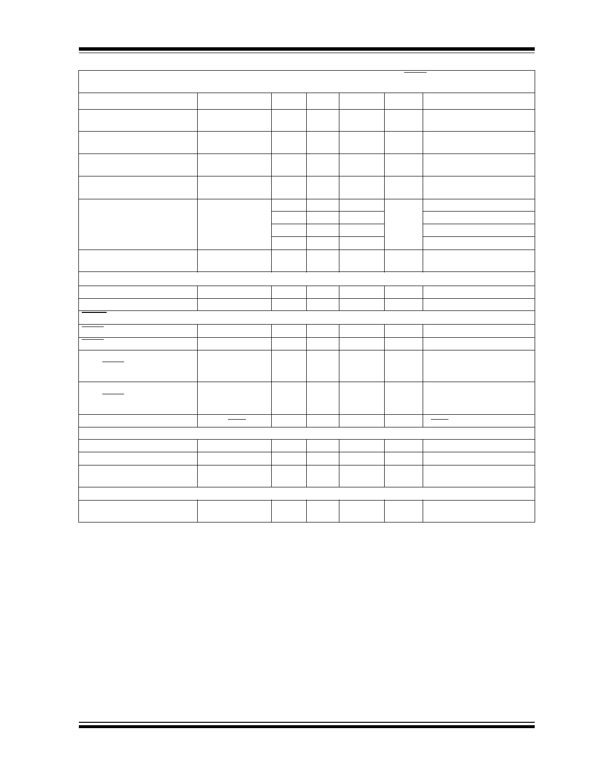
TC1307
VOUT Temperature Coefficient
LDO1/LDO2/LDO3/LDO4
TCV
OUT
—
20
40
—
ppm/°C Note 3
Line Regulation LDO1/LDO2/
LDO3/LDO4
∆
V
OUT
/(V
OUT
x
∆
V
IN
)
—
0.05
0.2
%/V
(V
R
+1)
≤
V
IN
≤
6.0V
Load Regulation
LDO1/LDO2/LDO3/LDO4
∆
V
OUT
/V
OUT
—
—
2.0
%
I
L
= 0.1 mA to I
OUT_MAX
Note 4
Thermal Regulation
LDO1/LDO2/LDO3/LDO4
∆
V
OUT
/
∆
P
D
—
0.04
—
V/W
Note 5
Dropout Voltage
LDO1/LDO2/LDO3/LDO4
V
IN
-V
OUT
—
2
—
mV
I
L
= 100 µA, Note 6
—
15
—
I
L
= 20 mA, Note 6
—
35
90
I
L
= 50 mA, Note 6
—
100
280
I
L
= 150 mA, Note 6
Output Noise
LDO1/LDO2/LDO3/LDO4
e
N
—
1.2
—
µV/(Hz)
½
I
OUT
= 100 mA, f = 10 kHz
C
OUT
= 1 µF to noise
Over Temperature Protection Characteristics:
Thermal Shutdown Protection
T
SD
—
150
—
°C
Note 7
Thermal Shutdown Hysteresis
∆
TSD
—
10
—
°C
SHDN Input Characteristics:
SHDN Input High Threshold
V
IH
60
—
—
% of V
IN
V
IN
= 2.7V to 6.0V
SHDN Input Low Threshold
V
IL
—
—
15
% of V
IN
V
IN
= 2.7V to 6.0V
Wake-up Time
(from SHDN mode)
t
WK
—
10
—
µsec
V
IN
= 5V, I
L
= 100 mA,
C
OUT
= 1 µF, C
IN
= 1 µF,
see Figure 4-1
Settling Time
(from SHDN mode)
t
S
—
40
—
µsec
V
IN
= 5V, I
L
= 100 mA,
C
OUT
= 1 µF, C
IN
= 1 µF,
See Figure 4-1
Shutdown Leakage Current
I
SHDN
—
±0.01
—
nA
V
SHDN
= V
IN
or GND
SELECT Input Characteristics:
SELECT Input High Threshold
V
SELH
V
IN
-0.2
—
—
V
V
IN
= 2.7V to 6.0V
SELECT Input Low Threshold
V
SELL
—
—
0.2
V
V
IN
= 2.7V to 6.0V
SELECT Input Leakage
Current
I
SELECT
—
—
±0.11
±0.06
—
—
µA
V
SELECT
= V
IN
V
SELECT
= GND
RESET Output Characteristics:
Detect Operating
Voltage Range
V
DET
1.0
1.2
—
—
6.0
6.0
V
T
A
= 0°C to +70°C
T
A
= -40°C to +125°C
Unless otherwise specified, all limits are established for V
IN
= V
R
+1, I
L
= 100 µA, C
L
= 3.3 µF, SHDN > V
IH
, T
A
= 25°C.
Boldface type specifications apply for junction temperatures, T
J
(Note 9) of -40°C to +125°C.
Parameter
Sym
Min
Typ
Max
Units
Conditions
Note 1: The minimum V
IN
must meet two conditions: V
IN
≥
2.7V and V
IN
≥
(V
R
+ 2.5%) + V
DROPOUT
.
2: V
R
is the nominal regulator output voltage. For example: V
R
= 1.8V, 2.5V, 2.8V or 3.0V.
3: TCV
OUT
= (V
OUT-HIGH
- V
OUT-LOW
) * 10
6
/ (V
R
*
∆
Temperature), V
OUT-HIGH
= Highest voltage measured over the tempera-
ture range. V
OUT-LOW
= Lowest voltage measured over the temperature range.
4: Load regulation is measured at a constant junction temperature using low duty cycle pulse testing. Load regulation is
tested over a load range from 1mA to the maximum specified output current. Changes in output voltage due to heating
effects are determined using thermal regulation specification TCV
OUT
.
5: Thermal regulation is defined as the change in output voltage at a time t after a change in power dissipation is applied.
Specifications are for a current pulse equal to I
LMAX
at V
IN
= 6.0V for t = 10 msec.
6: Dropout voltage is defined as the input to output differential at which the output voltage drops 2% below its nominal value
with a 1V differential applied.
7: The maximum allowable power dissipation is a function of ambient temperature, the maximum allowable junction temper-
ature and the thermal resistance from junction to air. (i.e. T
A
, T
J
,
θ
JA
). Exceeding the maximum allowable power dissipa-
tion will cause the device operating junction temperature to exceed the maximum 150°C rating. Sustained junction
temperatures above 150°C can impact the device reliability.
8: V
TH-MIN
= 2.55V and V
TH-MAX
= 2.70V.
9: The Junction temperature is approximated by soaking the device under test at an ambient temperature equal to the
desired Junction temperature. The test time is small enough such that the rise in the Junction temperature over the Ambi-
ent temperature is not significant.
TC1307
DS21702A-page 4
2002 Microchip Technology Inc.
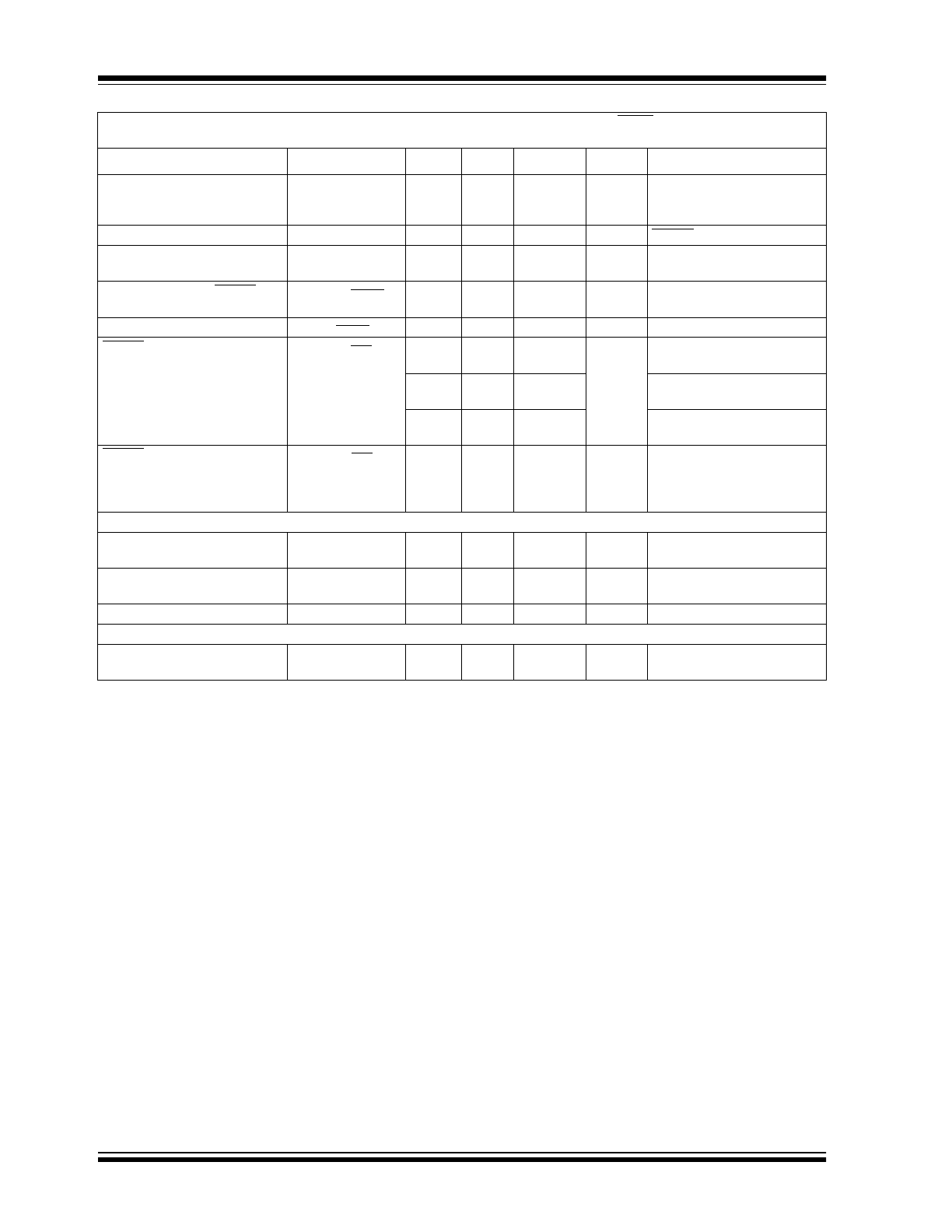
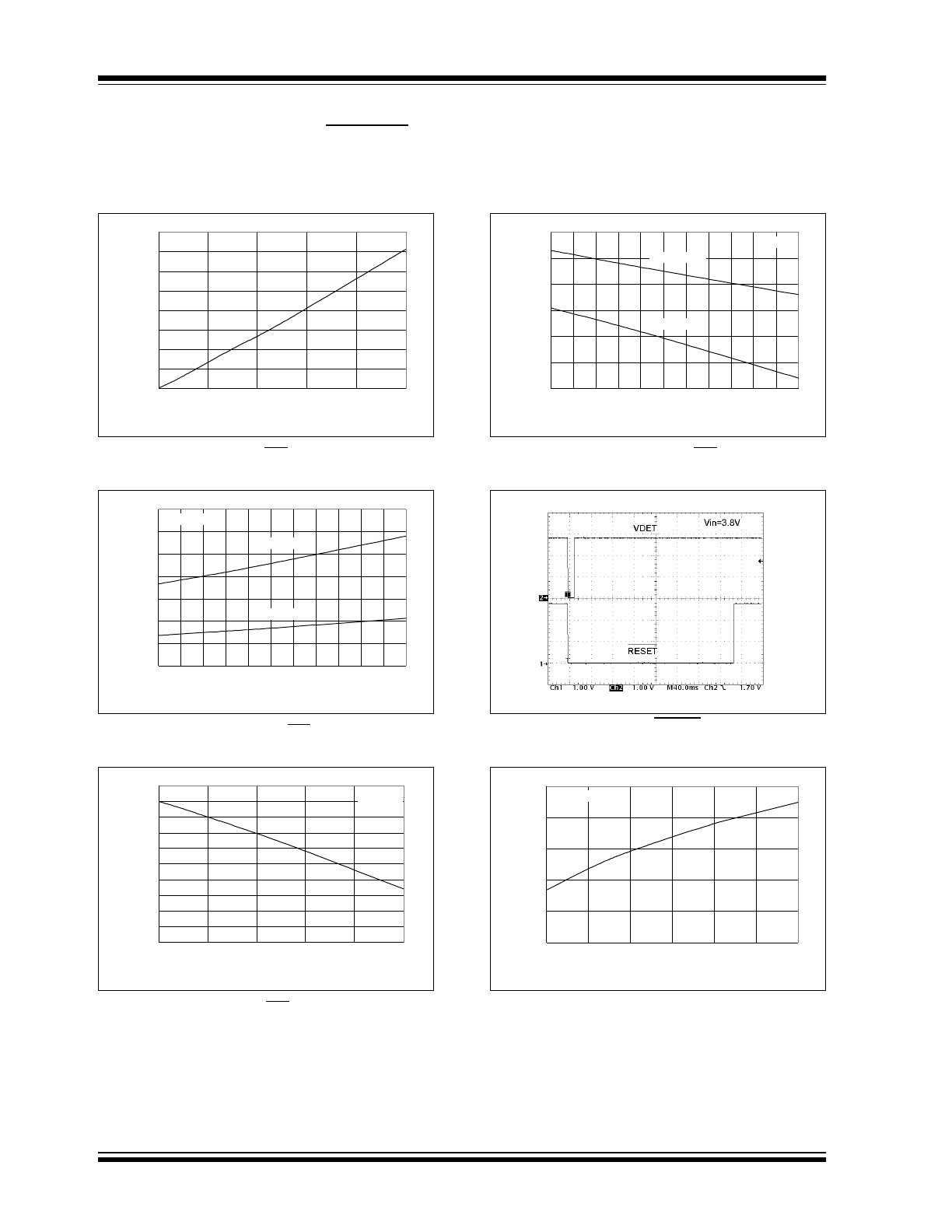
Reset Threshold Voltage
V
TH
2.59
2.55
2.63
—
2.66
2.70
V
V
T
A
= +25°C
T
A
= -40°C to +125°C
See Figure 4-2
Reset Circuit Supply Current
I
VDET
—
20
40
µA
RESET = Open
Reset Threshold Voltage
Temperature Coefficient
V
TH-TEMP
—
30
—
ppm/°C
Detect Threshold to RESET
Active Time Delay
T
VDET-RESET
—
135
—
µsec
V
DET
= V
TH
to V
TH
- 100 mV,
See Figure 4-2
Reset Time-out Period
T
RESET
140
300
560
msec
See Figure 4-2
RESET Output Voltage Low
V
OL-RES
—
—
0.3
V
V
DET
= V
TH-min
I
SINK
= 1.2 mA
—
—
0.4
V
DET
= V
TH-min
I
SINK
= 3.2 mA
—
—
0.3
V
DET
> 1.0V I
SINK
= 50 µA
Note 8, See Figure 4-2
RESET Output Voltage High
V
OH-RES
0.8*V
DET
V
DET
-
1.5V
—
—
V
I
SOURCE
= 500 µA
Isource = 800 µA
V
DET
>V
TH-max
(Both cases),
See Figure 4-2
Temperature Ranges:
Maximum Junction Temperature
Range
T
J
-40
—
+150
°C
Maximum Junction Temperature
Range
T
J
-40
—
+125
°C
Storage Temperature Range
T
A
-65
—
+150
°C
Thermal Package Resistances:
Thermal Resistance, 16L-QSOP
θ
JA
—
112.4
—
°C/W
EIA/JEDEC JESD51-751-7
4 Layer Board
Unless otherwise specified, all limits are established for V
IN
= V
R
+1, I
L
= 100 µA, C
L
= 3.3 µF, SHDN > V
IH
, T
A
= 25°C.
Boldface type specifications apply for junction temperatures, T
J
(Note 9) of -40°C to +125°C.
Parameter
Sym
Min
Typ
Max
Units
Conditions
Note 1: The minimum V
IN
must meet two conditions: V
IN
≥
2.7V and V
IN
≥
(V
R
+ 2.5%) + V
DROPOUT
.
2: V
R
is the nominal regulator output voltage. For example: V
R
= 1.8V, 2.5V, 2.8V or 3.0V.
3: TCV
OUT
= (V
OUT-HIGH
- V
OUT-LOW
) * 10
6
/ (V
R
*
∆
Temperature), V
OUT-HIGH
= Highest voltage measured over the tempera-
ture range. V
OUT-LOW
= Lowest voltage measured over the temperature range.
4: Load regulation is measured at a constant junction temperature using low duty cycle pulse testing. Load regulation is
tested over a load range from 1mA to the maximum specified output current. Changes in output voltage due to heating
effects are determined using thermal regulation specification TCV
OUT
.
5: Thermal regulation is defined as the change in output voltage at a time t after a change in power dissipation is applied.
Specifications are for a current pulse equal to I
LMAX
at V
IN
= 6.0V for t = 10 msec.
6: Dropout voltage is defined as the input to output differential at which the output voltage drops 2% below its nominal value
with a 1V differential applied.
7: The maximum allowable power dissipation is a function of ambient temperature, the maximum allowable junction temper-
ature and the thermal resistance from junction to air. (i.e. T
A
, T
J
,
θ
JA
). Exceeding the maximum allowable power dissipa-
tion will cause the device operating junction temperature to exceed the maximum 150°C rating. Sustained junction
temperatures above 150°C can impact the device reliability.
8: V
TH-MIN
= 2.55V and V
TH-MAX
= 2.70V.
9: The Junction temperature is approximated by soaking the device under test at an ambient temperature equal to the
desired Junction temperature. The test time is small enough such that the rise in the Junction temperature over the Ambi-
ent temperature is not significant.
2002 Microchip Technology Inc.
DS21702A-page 5
TC1307
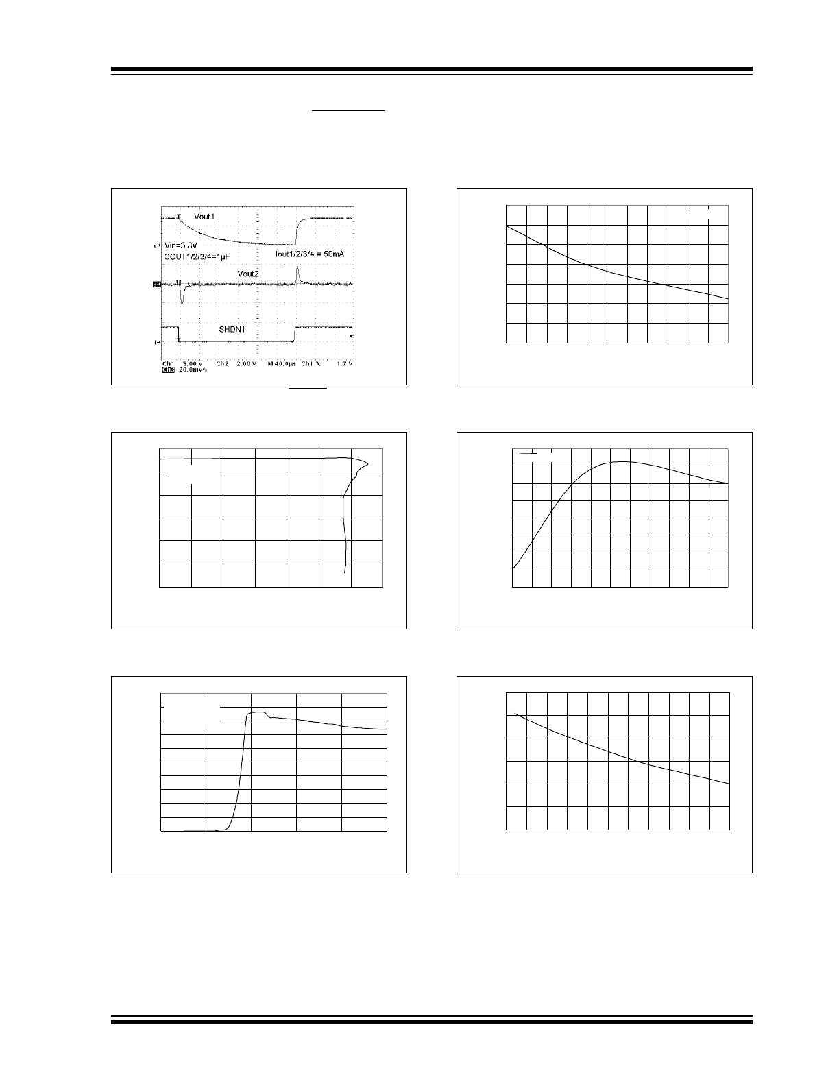
2.0
TYPICAL PERFORMANCE CHARACTERISTICS
Note: Unless otherwise indicated, V
IN
= 3.8V, C
IN
= 10 µF ceramic (X5R), C
OUT
= 1 µF ceramic (X5R), I
LOAD
= 100 µA,
SELECT12 = NC, SELECT34 = V
IN
, SHDN1/2/3/4 = V
IN,
T
A
= 25°C.
Junction temperature (T
J
) is approximated by soaking the device under test at an ambient temperature equal to the
desired Junction temperature. The test time is small enough such that the rise in the Junction temperature over the
Ambient temperature is not significant.
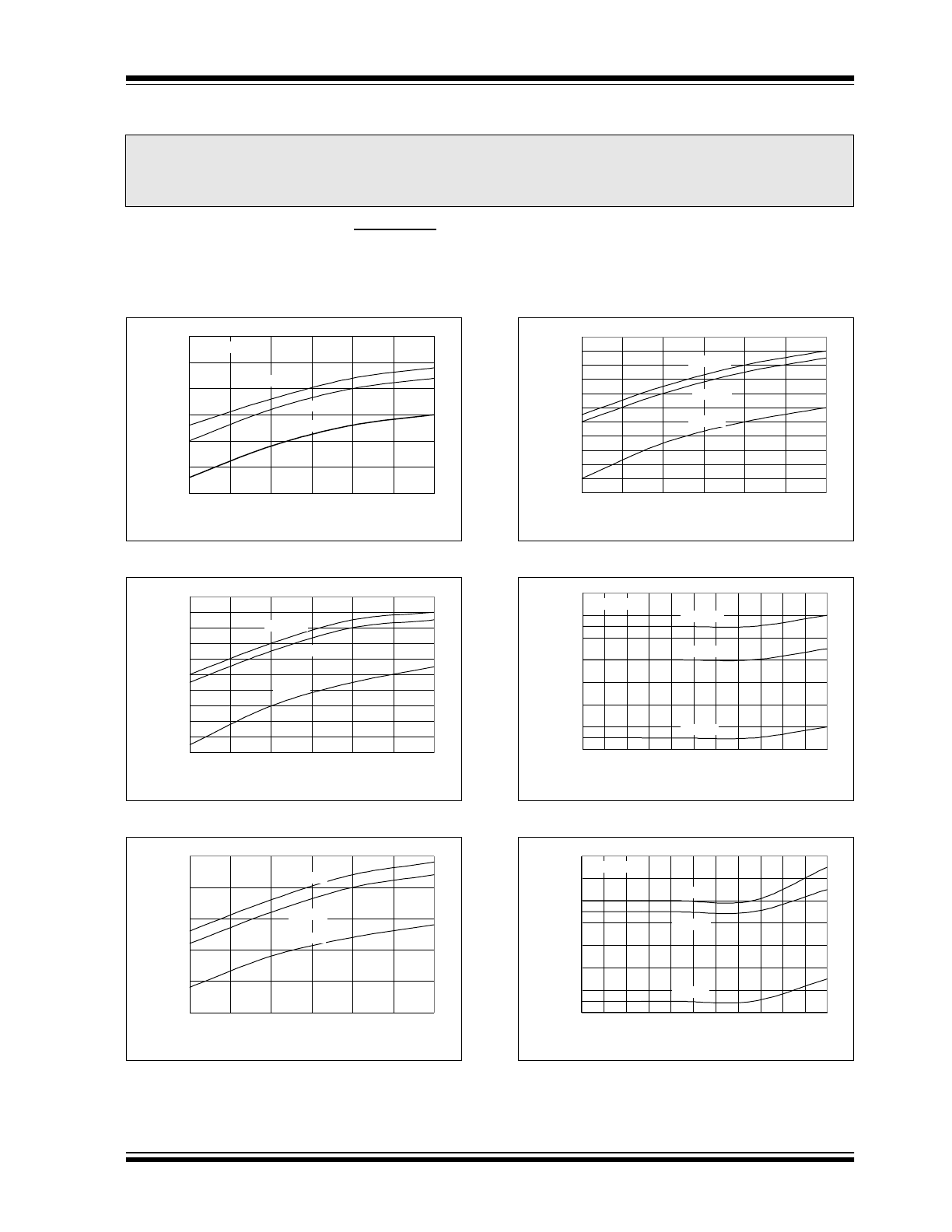
FIGURE 2-1:
V
OUT
vs. Load Current.
FIGURE 2-2:
V
OUT
vs. Load Current.
FIGURE 2-3:
V
OUT
vs. Load Current.
FIGURE 2-4:
V
OUT
vs. Load Current.
FIGURE 2-5:
V
OUT
vs. Input Voltage.
FIGURE 2-6:
V
OUT
vs. Input Voltage.
Note:
The graphs and tables provided following this note are a statistical summary based on a limited number of
samples and are provided for informational purposes only. The performance characteristics listed herein
are not tested or guaranteed. In some graphs or tables, the data presented may be outside the specified
operating range (e.g., outside specified power supply range) and therefore outside the warranted range.
1.800
1.805
1.810
1.815
1.820
1.825
1.830
0
25
50
75
100
125
150
Load Current (mA)
Output Voltage (V)
V
IN
= 2.8V
T
J
= +125°C
T
J
= +25°C
T
J
= -40°C
2.488
2.490
2.492
2.494
2.496
2.498
2.500
2.502
2.504
2.506
2.508
0
25
50
75
100
125
150
Load Current (mA)
Output Voltage (V)
V
IN
= 3.5V
T
J
= +125°C
T
J
= +25°C
T
J
= -40°C
2.78
2.785
2.79
2.795
2.8
2.805
0
25
50
75
100
125
150
Load Current (mA)
Output Voltage (V)
V
IN
= 3.8V
T
J
= +125°C
T
J
= +25°C
T
J
= -40°C
2.978
2.980
2.982
2.984
2.986
2.988
2.990
2.992
2.994
2.996
2.998
3.000
0
25
50
75
100
125
150
Load Current (mA)
Output Voltage (V)
V
IN
= 4.0V
T
J
= +125°C
T
J
= +25°C
T
J
= -40°C
1.802
1.804
1.806
1.808
1.810
1.812
1.814
1.816
2.7
3.0
3.3
3.6
3.9
4.2
4.5
4.8
5.1
5.4
5.7
6.0
Input Voltage (V)
Output Voltage (V)
I
LOAD
= 100 µA
T
J
= +125°C
T
J
= +25°C
T
J
= -40°C
2.488
2.49
2.492
2.494
2.496
2.498
2.5
2.502
2.7
3.0
3.3
3.6
3.9
4.2
4.5
4.8
5.1
5.4
5.7
6.0
Input Voltage (V)
Output Voltage (V)
I
LOAD
= 100 µA
T
J
= +125°C
T
J
= +25°C
T
J
= -40°C
TC1307
DS21702A-page 6
2002 Microchip Technology Inc.
Note: Unless otherwise indicated, V
IN
= 3.8V, C
IN
= 10 µF ceramic (X5R), C
OUT
= 1 µF ceramic (X5R), I
LOAD
= 100 µA,
SELECT12 = NC, SELECT34 = V
IN
, SHDN1/2/3/4 = V
IN,
T
A
= 25°C.
Junction temperature (T
J
) is approximated by soaking the device under test at an ambient temperature equal to the
desired Junction temperature. The test time is small enough such that the rise in the Junction temperature over the
Ambient temperature is not significant.
FIGURE 2-7:
V
OUT
vs. Input Voltage.
FIGURE 2-8:
V
IN
Supply Current vs. Junction
Temperature.
FIGURE 2-9:
Supply Current vs. Input Voltage, V
IN
.
FIGURE 2-10: V
DET
Supply Current vs. Junction
Temperature.
FIGURE 2-11: V
DET
Supply Current vs. V
DET
Input
Voltage.
FIGURE 2-12: Supply Current vs. Junction
Temperature.
2.780
2.782
2.784
2.786
2.788
2.790
2.792
2.794
2.796
3.0
3.3
3.6
3.9
4.2
4.5
4.8
5.1
5.4
5.7
6.0
Input Voltage (V)
Output Voltage (V)
I
LOAD
= 100 µA
T
J
= +125°C
T
J
= +25°C
T
J
= -40°C
100
120
140
160
180
200
220
240
260
280
-40
-25
-10
5
20
35
50
65
80
95
110
125
Junction Temperature (°C)
I
IN
Supply Current (µA)
V
IN
= 3.8V
I
LOAD1/2/3/4
= 0 mA
180
210
240
270
2.7
3
3.3
3.6
3.9
4.2
4.5
4.8
5.1
5.4
5.7
6
Input Voltage (V)
I
IN
Supply Current (µA)
T
J
= +125°C
T
J
= +25°C
T
J
= -40°C
I
LOAD1/2/3/4
= 0 mA
15.0
17.0
19.0
21.0
23.0
25.0
27.0
29.0
-40
-25
-10
5
20
35
50
65
80
95
110 125
Junction Temperature (°C)
I
VDET
Supply Current (µA)
V
DET
= 2.8V
RESET = OPEN
0.0
5.0
10.0
15.0
20.0
25.0
30.0
0.0
1.0
2.0
3.0
4.0
5.0
6.0
V
DET
Input Voltage (V)
I
VDET
Supply Current (µA)
T
J
= -40°C
T
J
= +25°C
T
J
= +125°C
V
IN
= 0V
SHDN1/2/3/4 = 0V
0.00
0.20
0.40
0.60
0.80
1.00
1.20
1.40
-40
-25
-10
5
20
35
50
65
80
95
110 125
Junction Temperature (°C)
Shutdown Supply Current (µA)
V
IN
= 2.7V
V
IN
= 3.8V
V
IN
= 6.0V
SHDN1/2/3/4 = 0V
2002 Microchip Technology Inc.
DS21702A-page 7
TC1307
Note: Unless otherwise indicated, V
IN
= 3.8V, C
IN
= 10 µF ceramic (X5R), C
OUT
= 1 µF ceramic (X5R), I
LOAD
= 100 µA,
SELECT12 = NC, SELECT34 = V
IN
, SHDN1/2/3/4 = V
IN,
T
A
= 25°C.
Junction temperature (T
J
) is approximated by soaking the device under test at an ambient temperature equal to the
desired Junction temperature. The test time is small enough such that the rise in the Junction temperature over the
Ambient temperature is not significant.
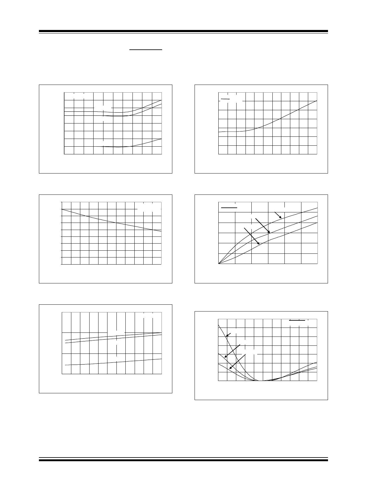
FIGURE 2-13: Dropout Voltage vs. Load Current.
FIGURE 2-14: Dropout Voltage vs. Load Current.
FIGURE 2-15: Crosstalk Characteristics V
OUT1
,
V
OUT2
and V
OUT3
.
FIGURE 2-16: Crosstalk Characteristics V
OUT1
,
V
OUT2
, and V
OUT3
.
FIGURE 2-17: Crosstalk Characteristics V
OUT1
,
V
OUT2
, and V
OUT3
.
FIGURE 2-18: Crosstalk Characteristics V
OUT1
,
V
OUT2
, and V
OUT3
.
0.000
0.020
0.040
0.060
0.080
0.100
0.120
0.140
0.160
0
25
50
75
100
125
150
Load Current (mA)
Droput Voltage (V)
T
J
= -40°C
T
J
= +25°C
T
J
= +125°C
V
OUT
= 2.8V
0.000
0.020
0.040
0.060
0.080
0.100
0.120
0.140
0
25
50
75
100
125
150
Load Current (mA)
Dropout Voltage (V)
T
J
= +40°C
T
J
= +25°C
T
J
= +125°C
V
OUT
= 3.0V
TC1307
DS21702A-page 8
2002 Microchip Technology Inc.
Note: Unless otherwise indicated, V
IN
= 3.8V, C
IN
= 10 µF ceramic (X5R), C
OUT
= 1 µF ceramic (X5R), I
LOAD
= 100 µA,
SELECT12 = NC, SELECT34 = V
IN
, SHDN1/2/3/4 = V
IN,
T
A
= 25°C.
Junction temperature (T
J
) is approximated by soaking the device under test at an ambient temperature equal to the
desired Junction temperature. The test time is small enough such that the rise in the Junction temperature over the
Ambient temperature is not significant.
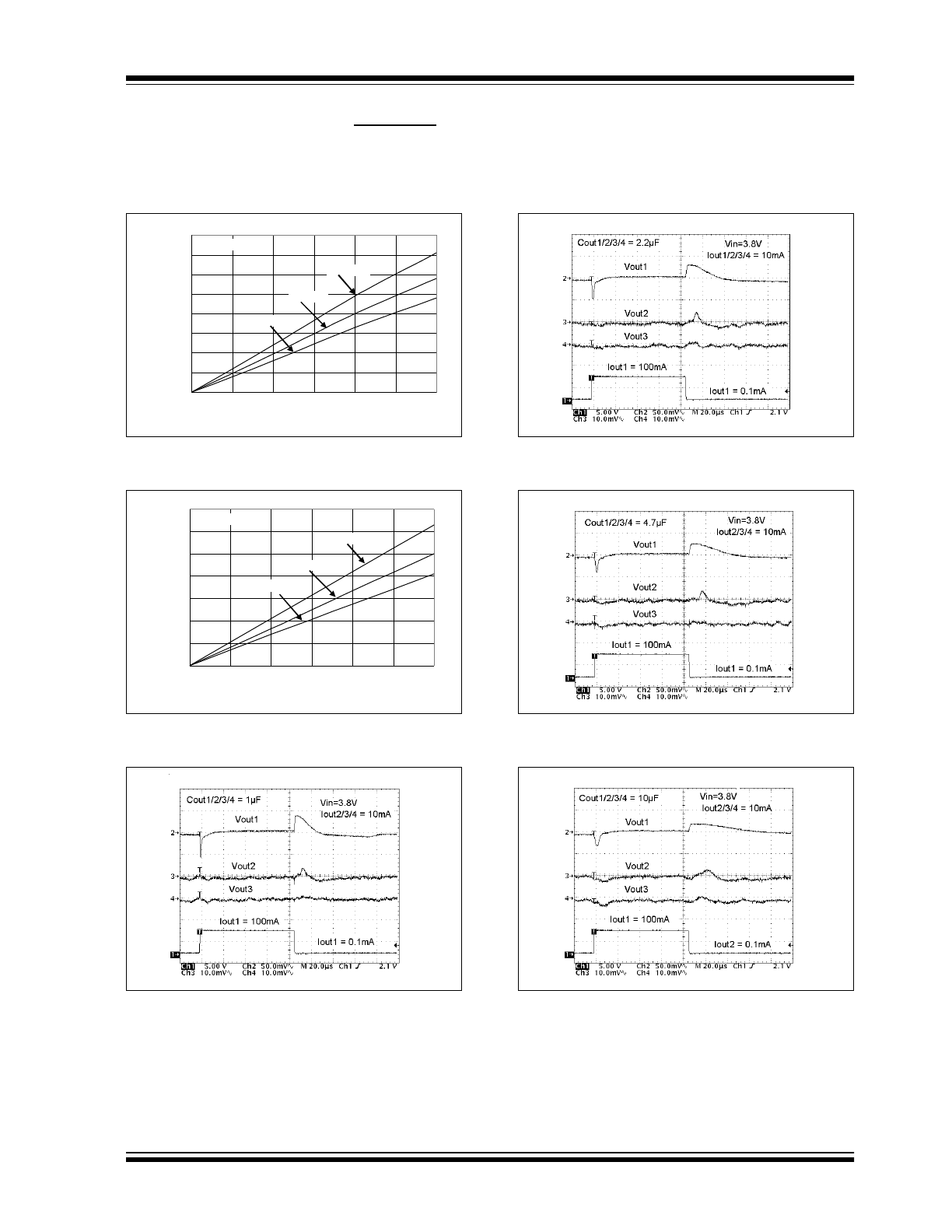
FIGURE 2-19: Line Step Response.
FIGURE 2-20: Line Step Response.
FIGURE 2-21: Power Supply Rejection Ratio vs.
Ripple Voltage Frequency.
FIGURE 2-22: Power Supply Rejection Ratio vs.
Ripple Voltage Frequency.
FIGURE 2-23: Output Noise.
FIGURE 2-24: Output Noise.
0
10
20
30
40
50
60
70
1.0E+01
1.0E+02
1.0E+03
1.0E+04
1.0E+05
1.0E+06
Ripple Voltage Frequency (Hz)
PSRR (dB)
V
IN
= 4.1V
V
OUT
= 2.8V
C
OUT
= 1 µF Ceramic
I
LOAD
= 100 mA
0
10
20
30
40
50
60
70
1.0E+01
1.0E+02
1.0E+03
1.0E+04
1.0E+05
1.0E+06
Ripple Voltage Frequency (Hz)
PSSR (dB)
V
IN
= 4.1V
V
OUT
= 2.8V
C
OUT
= 10µF Ceramic
I
LOAD
= 100 mA
2002 Microchip Technology Inc.
DS21702A-page 9
TC1307
Note: Unless otherwise indicated, V
IN
= 3.8V, C
IN
= 10 µF ceramic (X5R), C
OUT
= 1 µF ceramic (X5R), I
LOAD
= 100 µA,
SELECT12 = NC, SELECT34 = V
IN
, SHDN1/2/3/4 = V
IN,
T
A
= 25°C.
Junction temperature (T
J
) is approximated by soaking the device under test at an ambient temperature equal to the
desired Junction temperature. The test time is small enough such that the rise in the Junction temperature over the
Ambient temperature is not significant.
FIGURE 2-25: Response From SHDN.
FIGURE 2-26: Output Voltage vs. Current.
FIGURE 2-27: Short Circuit Current vs. Input Voltage.
FIGURE 2-28: Power-Up Reset Time-out Period vs.
Junction Temperature.
FIGURE 2-29: Reset Threshold Voltage vs. Junction
Temperature.
FIGURE 2-30: Reset Delay vs. Overdrive Voltage.
0
0.5
1
1.5
2
2.5
3
50
100
150
200
250
300
350
400
Output Current (mA)
Output Voltage (V)
C
OUT
= 1 µF
V
OUT
= Set to 2.8V
0
50
100
150
200
250
300
350
400
450
500
1
2
3
4
5
6
Input Voltage (V)
Short Circuit Current (mA)
C
OUT
= 1 µF
R
OUT
< 0.1 ohm
V
OUT
= Set to 2.8V
200
225
250
275
300
325
350
375
-40
-25
-10
5
20
35
50
65
80
95
110
125
Junction Temperature (°C)
Reset Delay Time (ms)
V
DET
= 0V to 2.7V
2.626
2.627
2.628
2.629
2.63
2.631
2.632
2.633
2.634
-40
-25
-10
5
20
35
50
65
80
95
110 125
Junction Temperature (°C)
Reset Threshold Voltage (V)
RESET = OPEN
40
60
80
100
120
140
160
0
0.1
0.2
0.3
0.4
0.5
0.6
0.7
0.8
0.9
1
1.1
Overdrive Voltage (V below V
TH
)
Time to Reset Output (µs)
TC1307
DS21702A-page 10
2002 Microchip Technology Inc.
Note: Unless otherwise indicated, V
IN
= 3.8V, C
IN
= 10 µF ceramic (X5R), C
OUT
= 1 µF ceramic (X5R), I
LOAD
= 100 µA,
SELECT12 = NC, SELECT34 = V
IN
, SHDN1/2/3/4 = V
IN,
T
A
= 25°C.
Junction temperature (T
J
) is approximated by soaking the device under test at an ambient temperature equal to the
desired Junction temperature. The test time is small enough such that the rise in the Junction temperature over the
Ambient temperature is not significant.
FIGURE 2-31: Reset V
OL-RES
vs. I
SINK
.
FIGURE 2-32: Reset V
OL-RES
vs. Junction
Temperature.
FIGURE 2-33: Reset V
OH-RES
vs. I
SOURCE
.
FIGURE 2-34: Reset V
OH-RES
vs.Junction
Temperature.
FIGURE 2-35: Power-Up RESET Timing.
FIGURE 2-36: Ground Current vs. Load Current.
0.00
0.10
0.20
0.30
0.40
0.50
0.60
0.70
0.80
0.0
2.0
4.0
6.0
8.0
10.0
Sink Current (mA)
Reset V
OL
(V)
V
DET
= 2.55V
0
0.05
0.1
0.15
0.2
0.25
0.3
0.35
-40
-25
-10
5
20
35
50
65
80
95
110 125
Junction Temperature (°C)
Reset V
OL
(V)
V
DET
= 2.55V
I
SINK
= 1.2 mA
I
SINK
= 3.2 mA
2.00
2.20
2.40
2.60
2.80
3.00
3.20
3.40
3.60
3.80
4.00
0.00
2.00
4.00
6.00
8.00
10.00
Source Current (mA)
Reset V
OH
(V)
V
DET
= 3.80V
5.91
5.92
5.93
5.94
5.95
5.96
5.97
-40
-25
-10
5
20
35
50
65
80
95
110 125
Junction Temperature (°C)
RESET V
OH
(V)
V
DET
= 6.0V
I
SOURCE
= 500 µA
I
SOURCE
= 800 µA
200
225
250
275
300
325
0
25
50
75
100
125
150
Load Current (mA)
Ground Current (µA)
V
DET
= V
IN
= 3 .8V