
2016 Microchip Technology Inc.
DS20005538B-page 1
SM813XXX
Features
• Generates Up to 8 Differential or Single-Ended
Outputs
• <65 fs Phase Jitter @ 156.25 MHz (1.875 MHz to
20 MHz)
• <115 fs Phase Jitter @ 156.25 MHz (12 kHz to
20 MHz)
• On-Chip Power Supply Regulation for Excellent
Power Supply Noise Immunity
• Two High-Performance PLL Synthesizers to
Generate Multiple Frequencies
• Independently Programmable Output Logic and
Frequency:
- Output Logic: LVPECL, LVDS, HCSL,
LVCMOS
• Fundamental Mode Crystal: 31.25 MHz to
156.250 MHz
• No External Crystal Oscillator Capacitors
Required
• 2.5V or 3.3V Operating Power Supply
• Separate Output Power Supplies:
- Each Bank can be at Different Power Supply
Voltage Levels (4 Banks of 2 Outputs Each)
• Industrial Temperature Range, –40°C to +85°C
• Green, RoHS-, and PFOS-Compliant 48-Pin
7 mm x 7 mm QFN Package
Applications
• 1/10/40/100 Gigabit Ethernet (GbE)
• SONET/SDH
• PCI-Express
• CPRI/OBSAI – Wireless Base Station
• Fibre Channel
• SAS/SATA
• DIMM (DDR2/DDR3/AMB)
• HDMI
General Description
The SM813xxx is a dual-PLL clock generator that
achieves ultra-low phase jitter (<65 fs
RMS
). With 8 total
outputs and dividers on each output, this device can
generate 8 different frequencies up to 850 MHz, from a
low-cost quartz crystal.
Each of 8 outputs can be independently programmed
to LVPECL, LVDS, HCSL, or LVCMOS logic. For
LVCMOS, only the true side of the channel is used.
The SM813xxx is packaged in a 48-pin QFN with up to
8 outputs.
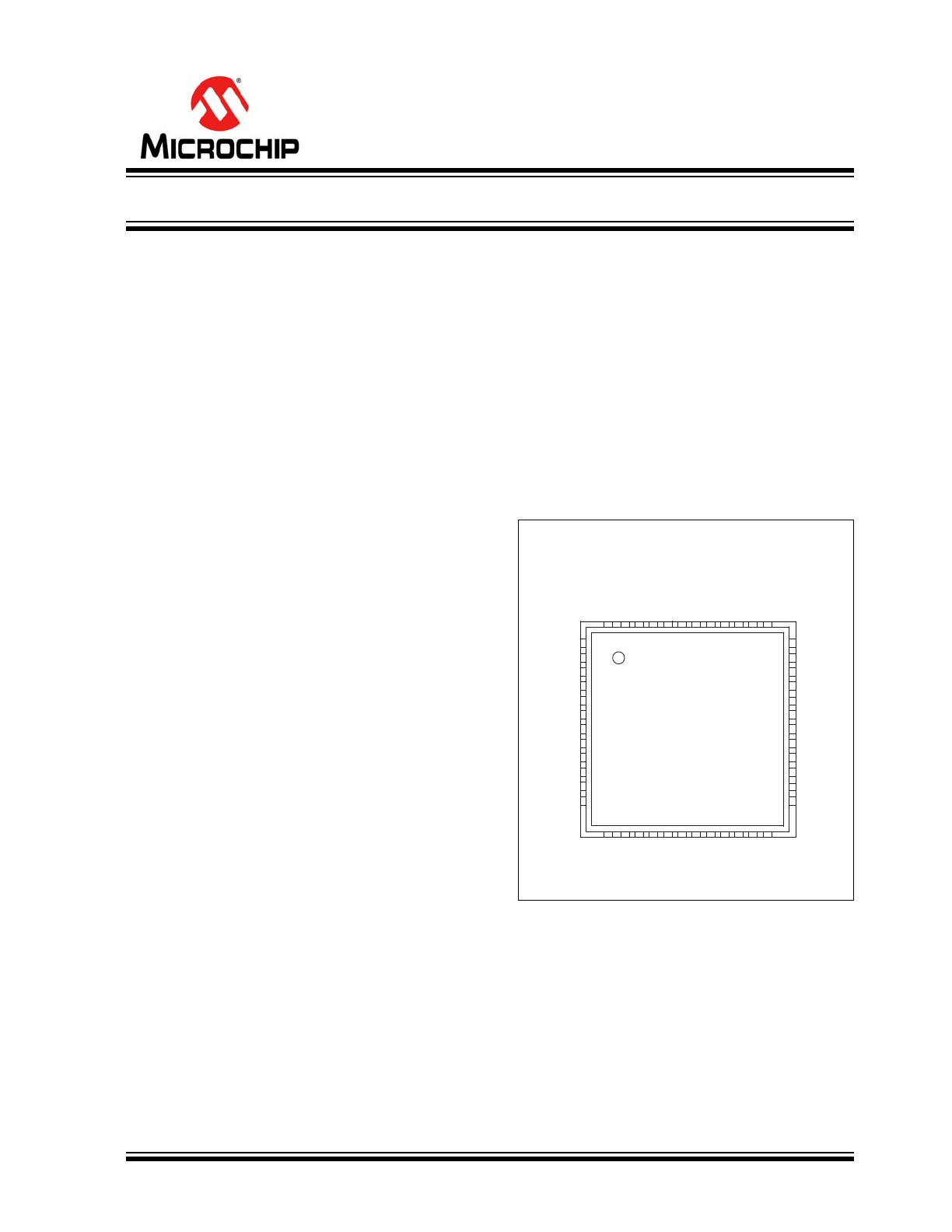
Package Type
1
2
3
4
5
6
7
8
14 15 16 17 18 19 20
48 47 46 45 44 43 42 41
VDDAP2
VDD
QC1
VDDOC
/QC1
QC2
/QC2
OEC
VDDI2
DNC
DNC
VSS
VSS
VDDI1 XIN XOUT
9
10
11
21 22 23
39
QD1
VDDOD
/QD1
40
38
VSS
DNC
DNC
SM813xxx
GND
/QD3
QD3
VDDOD
OED
DNC DNC
DNC
VDDOB
QB2
DNC
12
VSS
36
35
34
33
32
31
30
29
28
27
26
25
VDD
/QA1
QA1
VDDOA
/QA2
QA2
VDDOA
OEA
/QB1
QB1
VSS
OEB
24
/QB2
37
VDDAP1
13
SM813
XXX
48-Pin QFN (M)
Flexible Ultra-Low Jitter Clock Synthesizer
SM813XXX
DS20005538B-page 2
2016 Microchip Technology Inc.
Functional Block Diagram
PLL1
÷
÷
÷
÷
XO
QA1
QA2
QB1
QB2
PLL2
÷
÷
÷
÷
QC1
QC2
QD1
QD3
VDD POWER RAIL REGULATION
OTP MEMORY
2
VDD
1
VSS
OED
OEC
OEB
OEA
VSSOD
VSSOC
VSSOB
VSSOA
2 2 2
2
VDDOD
VDDOC
VDDOB
VDDOA
2 2 2
2
VSSAP2
VDDAP2
VSSAP1
VDDAP1
VSSI2
VDDI2
VSSI1
VDDI1
÷
÷
÷
÷
2016 Microchip Technology Inc.
DS20005538B-page 3
SM813XXX
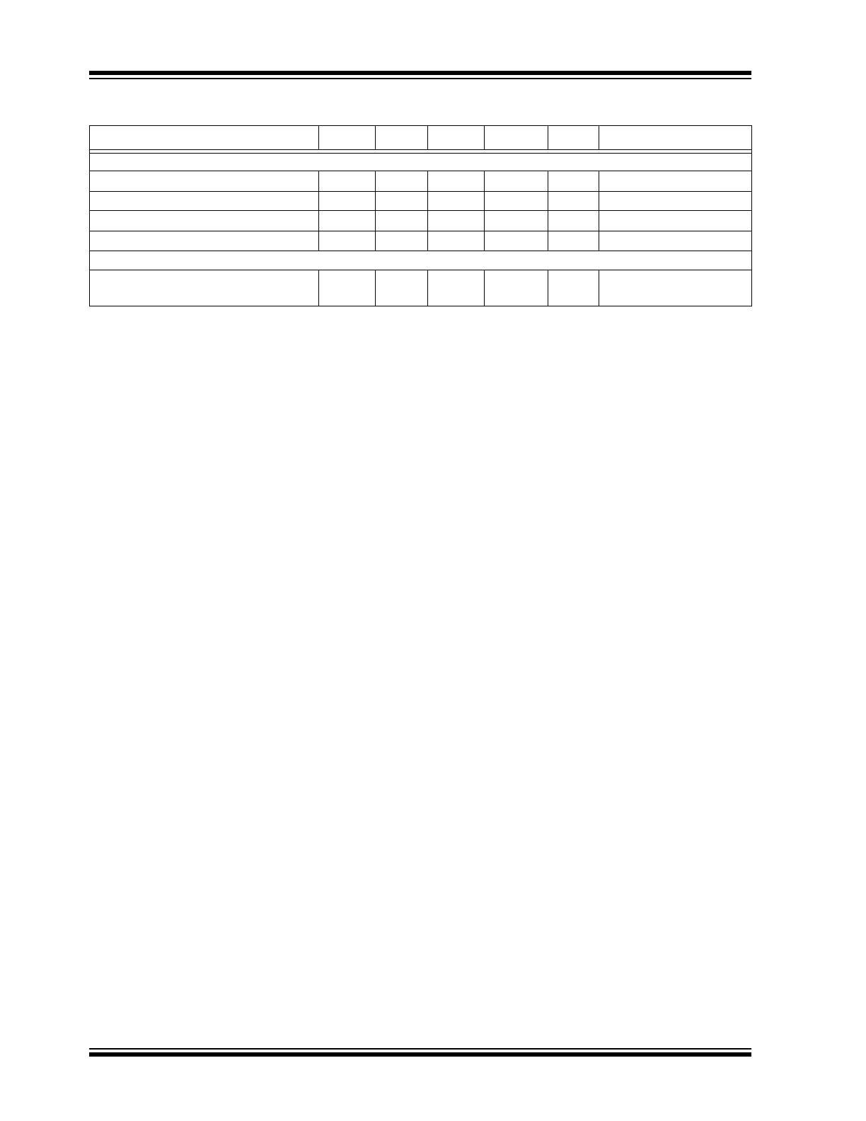
1.0
ELECTRICAL CHARACTERISTICS
Absolute Maximum Ratings †
Supply Voltage (V
DD
, V
DDA
, V
DDI
, V
DDO
).................................................................................................................+4.6V
Input Voltage (V
IN
) .................................................................................................................................. –0.50V to +4.6V
ESD Rating (MM)
(
1
)
..................................................................................................................................................200V
ESD Rating (HBM)
(
1
)
................................................................................................................................................. 2 kV
Operating Ratings ‡
Supply Voltage (V
DD
, V
DDO
) ............................................................................................................. +2.375V to +3.465V
†
Notice: Stresses above those listed under “Absolute Maximum Ratings” may cause permanent damage to the device.
This is a stress rating only and functional operation of the device at those or any other conditions above those indicated
in the operational sections of this specification is not intended. Exposure to maximum rating conditions for extended
periods may affect device reliability.
‡ Notice:
The device is not guaranteed to function outside its operating ratings.
Note 1:
Devices are ESD sensitive. Handling precautions are recommended. Human body model, 1.5 kΩ in series
with 100 pF.
Note 1:
Supply current may change depending on the device’s configuration.
TABLE 1-1:
ELECTRICAL CHARACTERISTICS
Electrical Characteristics:
Typical values are T
A
= +25°C, min./max. across –40°C ≤ T
A
≤ +85°C, unless otherwise
noted.
Symbol
Parameters
Min.
Typ.
Max.
Units
Condition
V
DD
,
V
DDO
Supply Voltage
2.375
2.5
2.625
V
2.5V Operation
3.135
3.3
3.465
3.3V Operation
V
DDI1
,
V
DDI2
Analog Supply Voltage
2.375
—
3.465
V
—
V
DDA
PLL Core Voltage
2.375
—
3.465
V
—
I
DDA
PLL Core Current Consumption
(
Note 1
)
—
—
60
mA
Per Active PLL
I
DDI
Analog Current Consumption
(
Note 1
)
—
—
10
mA
—
I
DDO
Output Stage Current
Consumption (
Note 1
)
—
—
70
mA
Per Output Bank,
Unloaded.
I
DD
Miscellaneous Logic
—
—
8
mA
—
SM813XXX
DS20005538B-page 4
2016 Microchip Technology Inc.
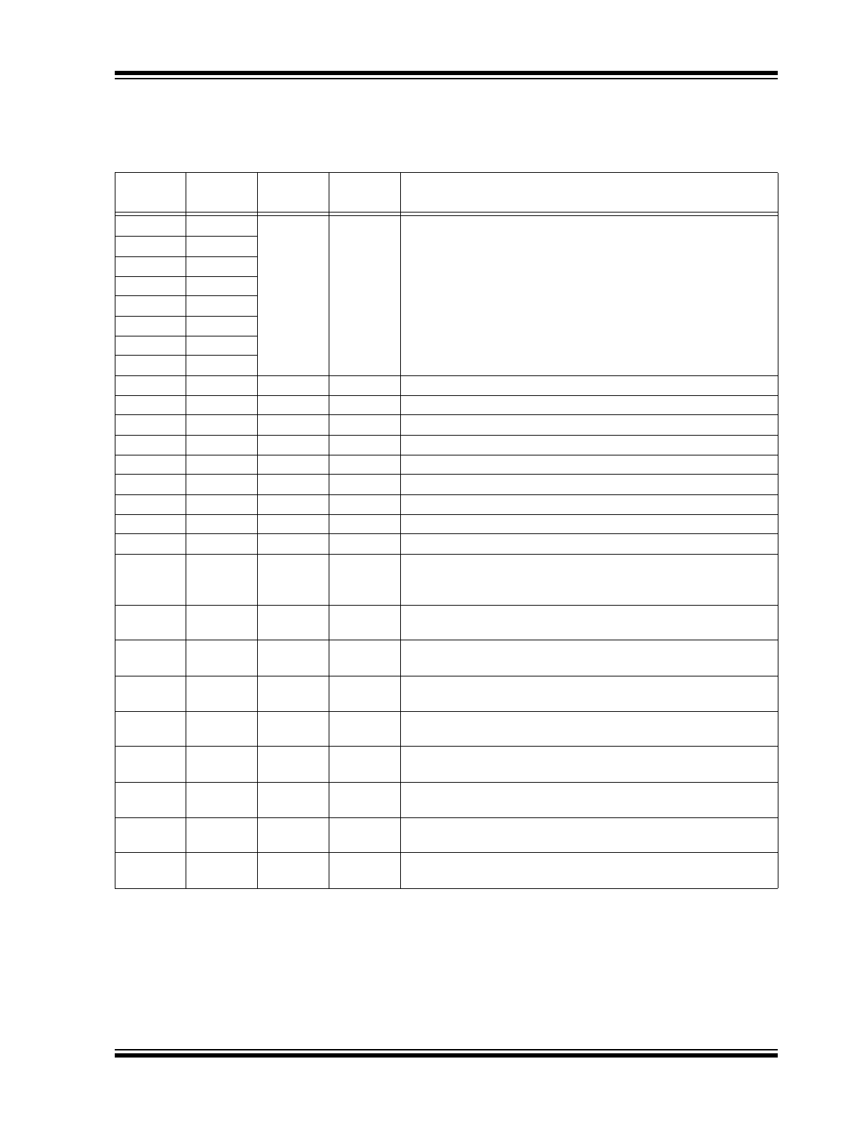
TABLE 1-2:
LVPECL DC ELECTRICAL CHARACTERISTICS
Electrical Characteristics:
V
DDCore
= V
DD
= V
DD0
= 3.3V ±5% or 2.5V ±5%, T
A
= –40°C to +85°C, unless otherwise
noted. R
L
= 50Ω to V
DDO
- 2V.
Symbol
Parameters
Min.
Typ.
Max.
Units
Conditions
V
OH
Output High Voltage
V
DDO
-
1.35
V
DDO
-
1.01
V
DDO
-
0.8
V
—
V
OL
Output Low Voltage
V
DDO
-
2
V
DDO
-
1.78
V
DDO
-
1.6
V
—
V
SWING
Peak-to-Peak Output Voltage
0.65
0.77
0.95
V
Figure 4-3
TABLE 1-3:
LVDS DC ELECTRICAL CHARACTERISTICS
Electrical Characteristics:
V
DDCore
= V
DD
= V
DD0
= 3.3V ±5% or 2.5V ±5%, T
A
= –40°C to +85°C, unless otherwise
noted. R
L
= 100Ω between Q and /Q.
Symbol
Parameters
Min.
Typ.
Max.
Units
Conditions
V
OD
Differential Output Voltage
245
350
530
mV
Figure 4-3
V
CM
Common Mode Voltage
1.125
1.2
1.375
V
—
V
OH
Output High Voltage
1.248
1.375
1.602
V
—
V
OL
Output Low Voltage
0.898
1.025
1.252
V
—
TABLE 1-4:
HCSL DC ELECTRICAL CHARACTERISTICS
Electrical Characteristics:
V
DDCore
= V
DD
= V
DD0
= 3.3V ±5% or 2.5V ±5%, T
A
= –40°C to +85°C, unless otherwise
noted. R
L
= 50Ω to V
SS
.
Symbol
Parameters
Min.
Typ.
Max.
Units
Conditions
V
OH
Output High Voltage
660
700
850
mV
—
V
OL
Output Low Voltage
–150
0
27
mV
—
V
CROSS
Crossing Point Voltage
—
350
—
V
—
TABLE 1-5:
LVCMOS DC ELECTRICAL CHARACTERISTICS
Electrical Characteristics:
V
DDCore
= V
DD
= V
DD0
= 3.3V ±5% or 2.5V ±5%, T
A
= –40°C to +85°C, unless otherwise
noted. R
L
= 50Ω to V
DDO
/2.
Symbol
Parameters
Min.
Typ.
Max.
Units
Conditions
V
OH
Output High Voltage
V
DD
-
0.8
—
—
V
Highest Drive (default)
V
OL
Output Low Voltage
—
—
0.5
V
—
V
IH
Input High Voltage
V
DD
-
0.7
—
V
DD
+
0.3
V
—
V
IL
Input Low Voltage
V
SS
-
0.3
—
0.3 x
V
DD
V
—
I
IH
Input High Current
—
—
5
µA
V
DD
= V
IN
= 3.465V
I
IL
Input Low Current
–150
—
—
µA
V
DD
= 3.465V, V
IN
= 0V
TABLE 1-6:
CRYSTAL CHARACTERISTICS
Parameters
Min.
Typ.
Max.
Units
Conditions
Mode of Oscillation
Fundamental, Parallel Resonant
—
Frequency
31.25
—
156.25
MHz
—
2016 Microchip Technology Inc.
DS20005538B-page 5
SM813XXX
Note 1:
See
Figure 4-6
.
2:
Output-to-output skew is defined as skew between outputs at the same supply voltage and with equal load
conditions. It is measured at the output differential crossing points.
3:
Output-to-output skew is only defined for outputs in the same PLL bank [A:B, C:D] with the same output logic
type setting.
4:
All phase noise measurements were taken with an Agilent 5052B phase noise system.
5:
Measured using a 52.0833 MHz crystal as the input reference source.
There are sufficient feedback dividers to support below 20 MHz, down to about 12 MHz, but phase noise performance
will be impacted. Please contact Microchip TCG Applications for more information.
Equivalent Series Resistance (ESR)
—
—
80
Ω
Saunders 250B,
25Ω Pi Network
Load Capacitance (C
L
)
—
8
—
pF
Device Equivalent Load
Shunt Capacitor, C0
—
1
2
pF
—
Correlation Drive Level
—
10
100
µW
—
TABLE 1-7:
AC ELECTRICAL CHARACTERISTICS
Electrical Characteristics:
V
DD
= V
DDO1/2
= 3.3V ±5% or 2.5V ±5%; V
DD
= 3.3V ±5%, V
DDO1/2
= 3.3V ±5% or 2.5V
±5%; T
A
= –40°C to +85°C.
Symbol
Parameters
Min.
Typ.
Max.
Units
Conditions
F
IN
Input Frequency
31.25
50
156.25
MHz
XO
F
OUT
Output Frequency
12
—
850
MHz
LVPECL, LVDS, HCSL
12
—
250
LVCMOS
t
r
/t
f
Output Rise/Fall Time (
Note 1
)
85
135
350
ps
LVPECL Output
85
140
300
LVDS Output
175
300
450
HCSL Output
100
200
400
LVCMOS Output
ODC
Output Duty Cycle
45
50
55
%
All Output Frequencies
48
50
52
<350 MHz Output Frequencies
T
SKEW
Output-to-Output Skew
(
Note 2
,
Note 3
)
—
—
50
ps
Note 3
, Same Output Bank
T
LOCK
PLL Lock Time
—
5
20
ms
V
DD
= 90%
T
jit(Ø)
RMS Phase Jitter (
Note 4
,
Note 5
)
—
112
150
fs
Integration Range 12 kHz -
20 MHz
—
64
—
Integration Range 1.875 MHz -
20 MHz
TABLE 1-6:
CRYSTAL CHARACTERISTICS (CONTINUED)
Parameters
Min.
Typ.
Max.
Units
Conditions
SM813XXX
DS20005538B-page 6
2016 Microchip Technology Inc.
TEMPERATURE SPECIFICATIONS
Parameters
Sym.
Min.
Typ.
Max.
Units
Conditions
Temperature Ranges
Ambient Temperature
T
A
–40
—
+85
°C
Note 1
Storage Temperature Range
T
S
–65
—
+150
°C
—
Lead Temperature
—
—
—
+260
°C
Soldering, 20s
Case Temperature
—
—
—
+115
°C
—
Package Thermal Resistances
Junction Thermal Resistance QFN, Still
Air
JA
—
24
—
°C/W
—
Note 1:
The maximum allowable power dissipation is a function of ambient temperature, the maximum allowable
junction temperature and the thermal resistance from junction to air (i.e., T
A
, T
J
,
JA
). Exceeding the
maximum allowable power dissipation will cause the device operating junction temperature to exceed the
maximum +85°C rating. Sustained junction temperatures above +85°C can impact the device reliability.
2016 Microchip Technology Inc.
DS20005538B-page 7
SM813XXX
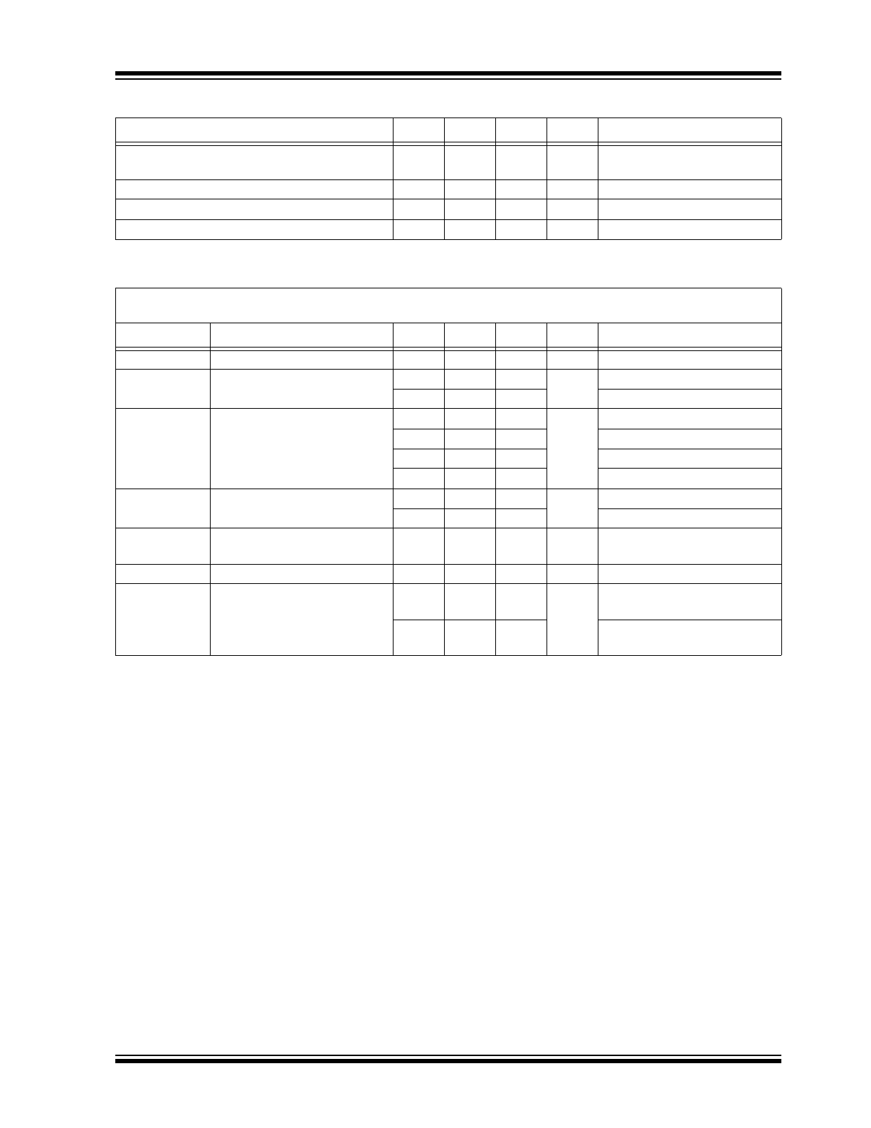
2.0
PIN DESCRIPTIONS
The descriptions of the pins are listed in
Table 2-1
.
TABLE 2-1:
PIN FUNCTION TABLE
Pin
Number
Pin Name
Pin Type
Pin Level
Description
34, 35
QA1, /QA1
O
(DIF, SE)
LVPECL
LVDS
HCSL
LVCMOS
(Q only)
Differential/Single-Ended Clock Output (LVCMOS)
31, 32
QA2, /QA2
27, 28
QB1, /QB1
22, 24
QB2, /QB2
3, 5
QC1, /QC1
6, 7
QC2, /QC2
9, 11
QD1, /QD1
15, 16
QD3, /QD3
2, 36
V
DD
PWR
—
Power Supply
30, 33
V
DDOA
PWR
—
Power Supply for Outputs QA1–2
23
V
DDOB
PWR
—
Power Supply for Outputs QB1–2
4
V
DDOC
PWR
—
Power Supply for Outputs QC1–2
10, 14
V
DDOD
PWR
—
Power Supply for Outputs QD1 and QD3
37
V
DDAP1
PWR
—
Power Supply for PLL1
1
V
DDAP2
PWR
—
Power Supply for PLL2
43
V
DDI1
PWR
3.3V Only Power Supply for Input Circuits
44
V
DDI2
PWR
3.3V Only Power Supply for Input Circuits
12, 26, 38
47, 48,
ePAD
V
SS
(Exposed
Pad)
PWR
—
Power Supply Ground. The exposed pad must be connected to
the V
SS
ground plane.
29
OEA1/2
I, (SE)
LVCMOS Output Enable, Outputs QA1/2 disable to tri-state,
0 = Disabled, 1 = Enabled, on-chip 75 kΩ pull-up
25
OEB1/2
I, (SE)
LVCMOS Output Enable, Outputs QB1/2 disable to tri-state,
0 = Disabled, 1 = Enabled, on-chip 75 kΩ pull-up
8
OEC1/2
I, (SE)
LVCMOS Output Enable, Outputs QC1/2 disable to tri-state,
0 = Disabled, 1 = Enabled, on-chip 75 kΩ pull-up
13
OED1/3
I, (SE)
LVCMOS Output Enable, Outputs QD1/3 disable to tri-state,
0 = Disabled, 1 = Enabled, on-chip 75 kΩ pull-up
42
XIN
I, (SE)
8 pF
Crystal
Crystal Reference Input, no load caps needed
41
XOUT
O, (SE)
8 pF
Crystal
Crystal Reference Output, no load caps needed
18, 19, 20,
21
DNC
DNC
—
Leave open; for normal operation, do not connect to anything.
17
GND
I
—
This pin is not Power Supply ground, but must be tied to V
SS
for
proper operation.
SM813XXX
DS20005538B-page 8
2016 Microchip Technology Inc.
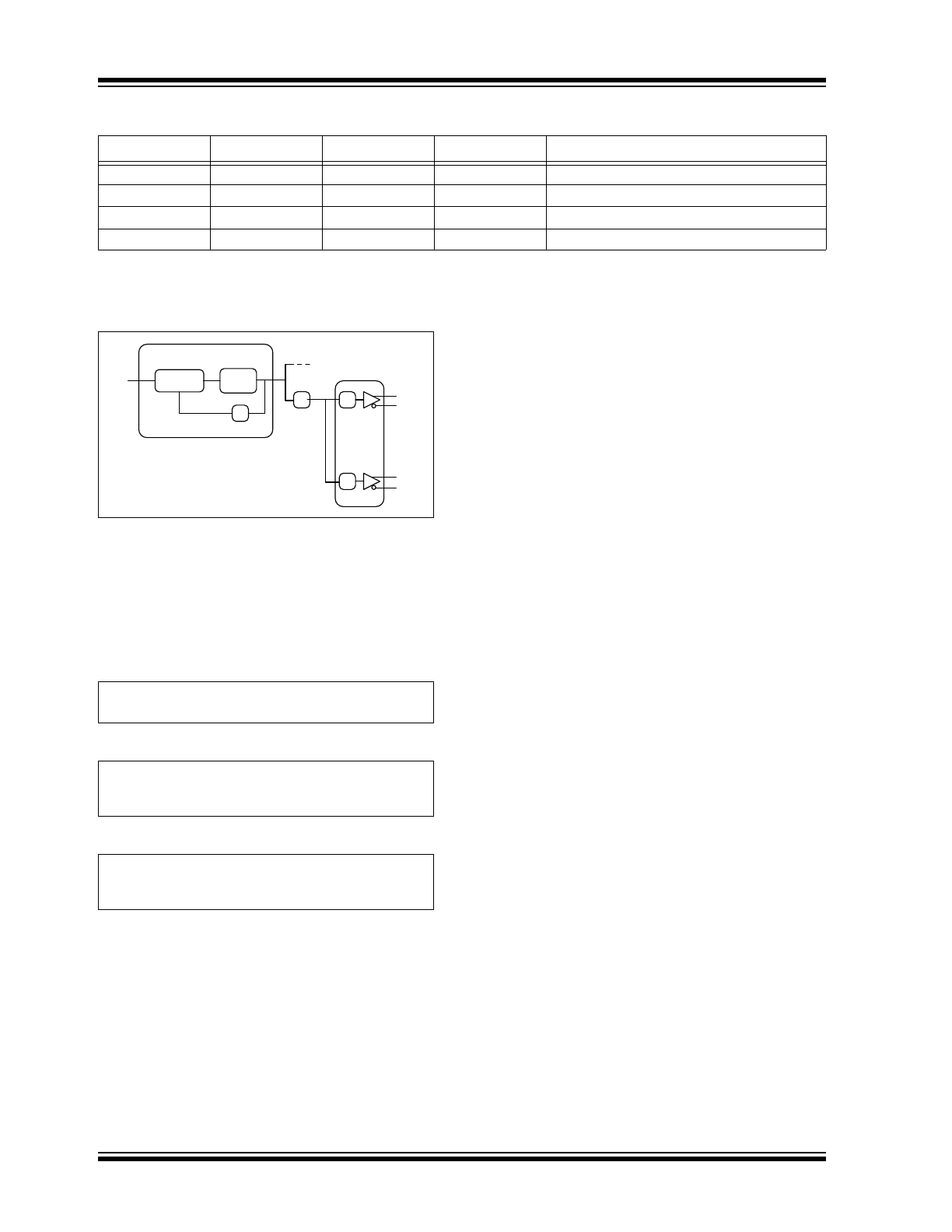
2.1
Key Programmable Parameters
FIGURE 2-1:
Frequency Settings for One
PLL and One Output Bank.
The VCO in the PLL has a range of ~2875 MHz to
3510 MHz.
Counters M and P0 have a range of 4 to 259.
Counters P1, P2, and P3 have a range of 1 to 16.
EQUATION 2-1:
EQUATION 2-2:
EQUATION 2-3:
2.1.1
OUTPUT LOGIC PROGRAMMING
Available output logic types are LVPECL, LVDS, HCSL,
and LVCMOS.
Each output can be programmed individually to one of
the four logic types.
All logic types are differential, except LVCMOS. For
LVCMOS, only the true channel of the output pair is
enabled and the complementary channel is disabled.
With LVCMOS there is also an output drive setting.
There is one setting for all LVCMOS outputs, so all
LVCMOS outputs will have the same drive strength.
Unused outputs are disabled to high impedance.
TABLE 2-2:
TRUTH TABLE
OEA
OEB
OEC
OED
Output
0
1
1
1
2 QA outputs tri-state
1
0
1
1
2 QB outputs tri-state
1
1
0
1
2 QC outputs tri-state
1
1
1
0
2 QD outputs tri-state
÷
÷
QD1
QD3
÷
REF
PLL
÷
VCO
PHASE
DETECTOR
M
P0
P1
P2
P3
F
VCO
REF
M
=
QD1
F
VCO
P0
P1
=
QD3
F
VCO
P0
P3
=
2016 Microchip Technology Inc.
DS20005538B-page 9
SM813XXX
3.0
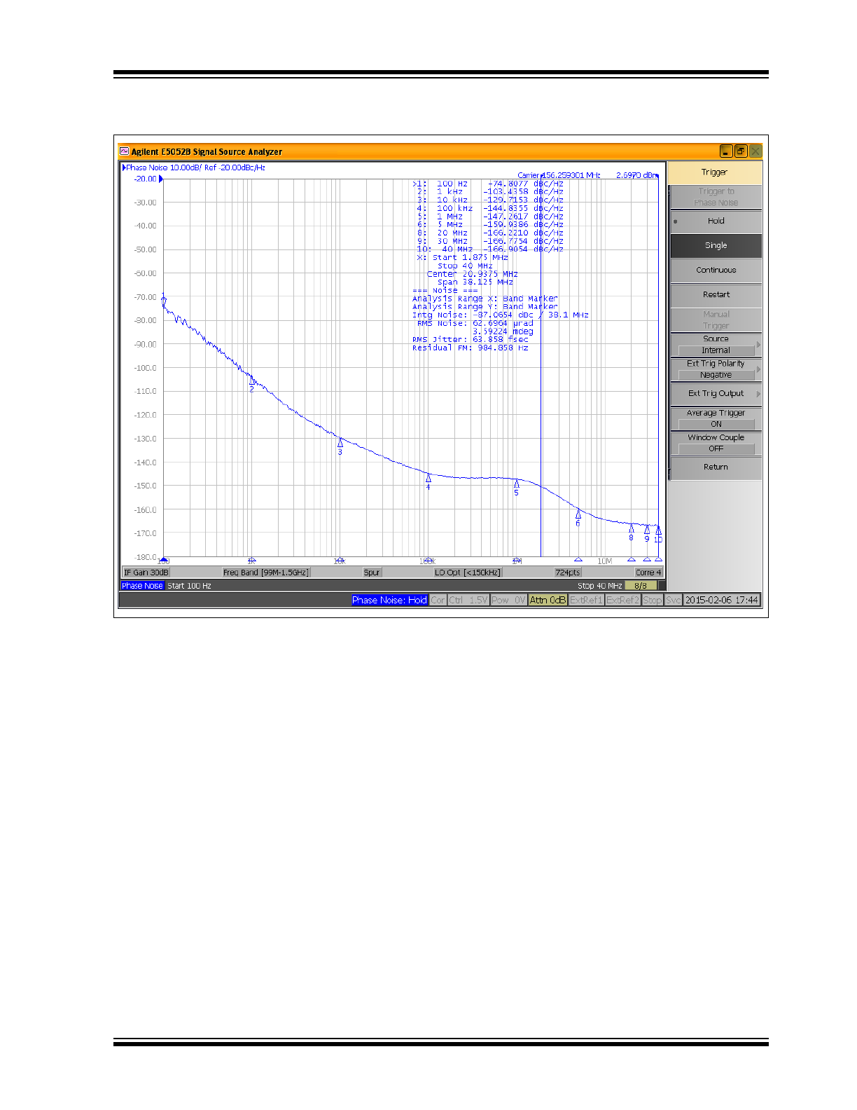
PHASE NOISE PERFORMANCE
FIGURE 3-1:
156.25 MHz, LVPECL Integration Range 1.875 MHz to 20 MHz: 64 fs
RMS
.
SM813XXX
DS20005538B-page 10
2016 Microchip Technology Inc.
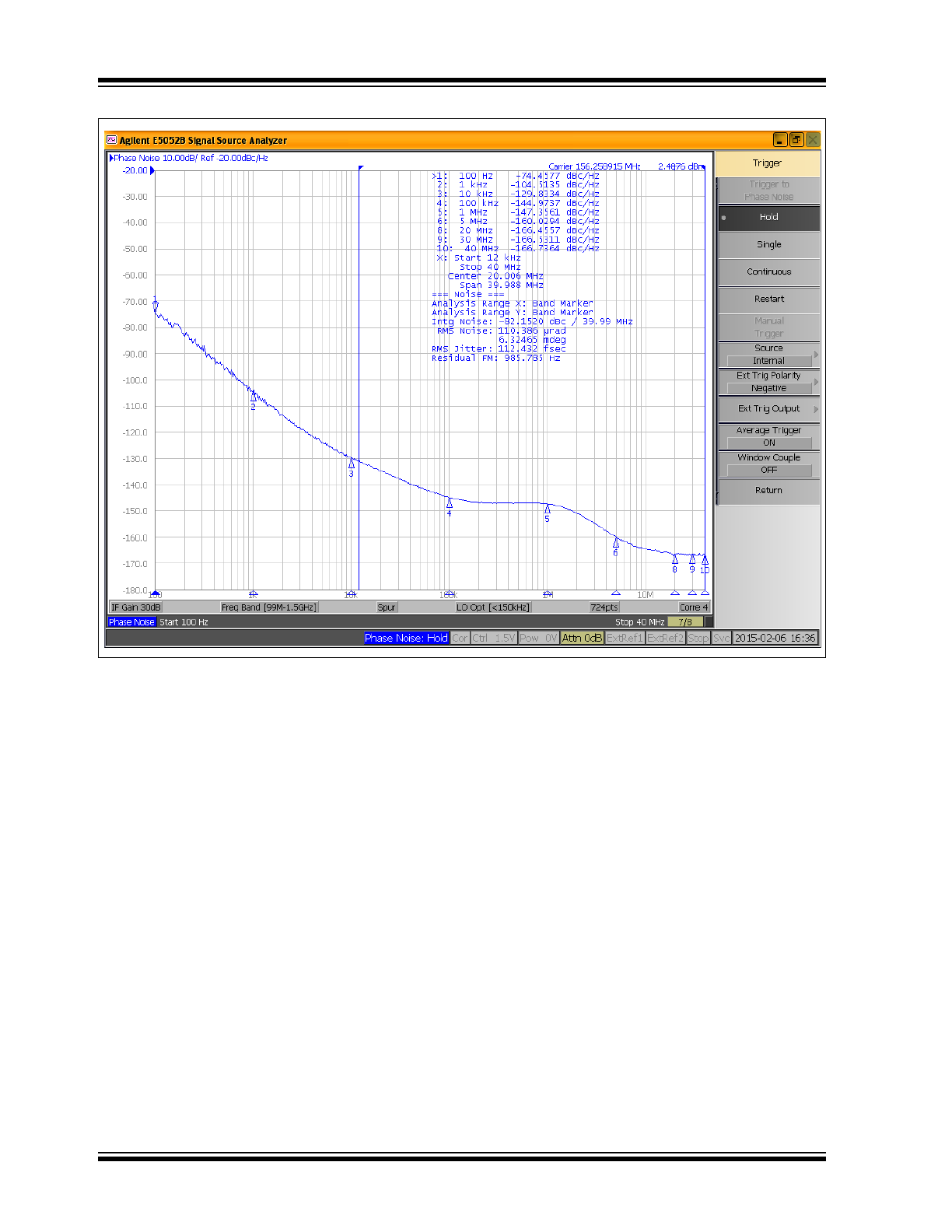
FIGURE 3-2:
156.25 MHz, LVPECL Integration Range 12 kHz to 40 MHz: 112.4 fs
RMS
.