

FDC37C78
Floppy Disk Controller
FEATURES
•
3.3/5 Volt Operation
•
Intelligent Auto Power Management
•
2.88MB FDC37C78 Floppy Disk Controller
-
Licensed CMOS 765B Floppy Disk
Controller
-
Software and Register Compatible with
SMSC's Proprietary 82077AA
Compatible Core
-
Supports Two Floppy Drives Directly
-
Supports Vertical Recording Format
-
16 Byte Data FIFO
-
100% IBM Compatibility
-
DMA Enable Logic
-
Data Rate and Drive Control Registers
-
Swap Drives A and B
-
Non-Burst Mode DMA Option
-
Detects All Overrun and Underrun
Conditions
-
Sophisticated Power Control Circuitry
(PCC) Including Multiple Powerdown
Modes for Reduced Power
Consumption
•
Enhanced Digital Data Separator
-
2 Mbps (Only Available When V
CC
= 5V),
1 Mbps, 500 Kbps, 300 Kbps, 250 Kbps
Data Rates
-
Programmable Precompensation Modes
•
48 pin TQFP Package

2
TABLE OF CONTENTS
FEATURES...............................................................................................................................................1
GENERAL DESCRIPTION .......................................................................................................................3
PIN CONFIGURATION.............................................................................................................................4
DESCRIPTION OF PIN FUNCTIONS ......................................................................................................6
FUNCTIONAL DESCRIPTION ...............................................................................................................10
FDC37C78
REGISTERS ..................................................................................................................10
HOST
PROCESSOR
INTERFACE ..................................................................................................10
FLOPPY
DISK
CONTROLLER .........................................................................................................11
FLOPPY DISK CONTROLLER INTERNAL REGISTERS.................................................................11
COMMAND SET/DESCRIPTIONS .........................................................................................................29
INSTRUCTION SET ...............................................................................................................................32
AUTO POWER MANAGEMENT.............................................................................................................58
CONFIGURATION..................................................................................................................................62
OPERATIONAL DESCRIPTION.............................................................................................................71
MAXIMUM
GUARANTEED RATINGS ..............................................................................................71
DC ELECTRICAL CHARACTERISTICS ...........................................................................................71
TIMING DIAGRAMS ...............................................................................................................................75

3
GENERAL DESCRIPTION
The SMSC FDC37C78 Floppy Disk Controller
utilizes SMSC's proven SuperCell technology
for increased product reliability and functionality.
The FDC37C78 optimized for motherboard
applications. The FDC37C78 supports both 1
Mbps and 2 Mbps data rates and vertical vertical
recording operation at 1 Mbps Data Rate.
The FDC37C78 incorporates SMSC's true CMOS
765B floppy disk controller, advanced digital data
separator, 16 byte data FIFO, on-chip 12 mA bus
drivers and two floppy direct drive support. The
true CMOS 765B core provides 100%
compatibility with IBM PC/XT and PC/AT
architectures in addition to providing data overflow
and underflow protection. The SMSC advanced
digital data separator incorporates SMSC's
patented data separator technology, allowing for
ease of testing and use.
The FDC37C78 incorporates sophisticated power
control circuitry (PCC). The PCC supports
multiple low power down modes.
The FDC37C78 Floppy Disk Controller
incorporates Software Configurable Logic (SCL)
for ease of use. Use of the SCL feature allows
programmable system configuration of key
functions of FDC
The FDC37C78 does not require any external
filter components, and is, therefore easy to use
and offers lower system cost and reduced board
area. The FDC37C78 is software and register
compatible with SMSC's proprietary 82077AA
core.
4
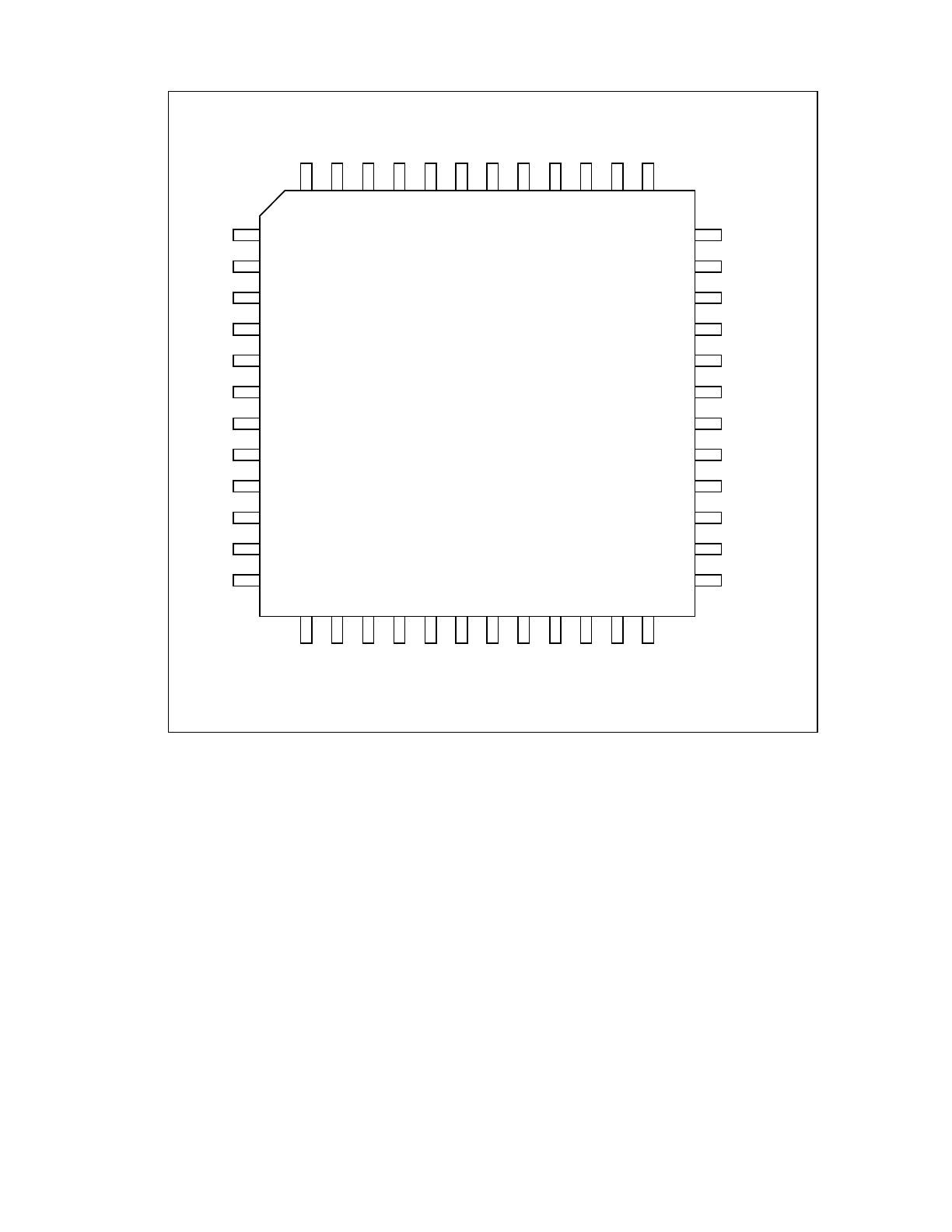
PIN CONFIGURATION
R
ESE
T
1
nDACK
D0
D1
D2
D3
VSS
VCC
D4
D5
D6
D7
VCC
FDC37C78
13
25
IR
Q
TC
nT
RK0
nI
ND
E
X
nW
R
T
P
R
T
VS
S
VC
C
nD
S
K
C
H
G
nRD
A
T
A
D
R
VD
EN
0
D
R
VD
EN
1
DE
N
S
E
L
MEDIA_ID0
MEDIA_ID1
nWDATA
nWGATE
nHDSEL
VSS
nSTEP
VCC
nDIR
nMTR1/IDLE
nDS1/PD
nMTR0
DRQ
nI
OW
nI
O
R
nC
S
A0
A1
A2
VS
S
X1
X2
nDS
0
2
3
4
5
6
7
8
9
10
11
12
14
15
16
17
18
19
20
21
22
23
24
36
35
34
33
32
31
30
29
28
27
26
37
38
39
40
41
42
43
44
45
46
47
48

5
FDC37C78 PIN OUT
FDC37C78 48 Pin FDC
PIN #
NAME
PIN #
NAME
1 nDACK
25 MEDIA_ID0
2 D0
26 MEDIA_ID1
3 D1
27 nWDATA
4 D2
28 nWGATE
5 D3
29 nHDSEL
6 VSS 30 VSS
7 VCC 31 nSTEP
8 D4
32 VCC
9 D5
33 nDIR
10 D6
34 nMTR1/IDLE
11 D7
35 nDS1/PD
12 VCC 36 nMTR0
13 IRQ
37 nDS0
14 TC
38 RESET
15 nTRK0 39 X2
16 nINDEX
40 X1
17 nWRTPRT
41 VSS
18 VSS 42 A2
19 VCC 43 A1
20 nDSKCHG
44 A0
21 nRDATA
45 nCS
22 DRVDEN0
46 nIOR
23 DRVDEN1
47 nIOW
24 DENSEL
48 DRQ
Note: “n” denotes active low signal.

6
DESCRIPTION OF PIN FUNCTIONS
DESCRIPTION OF PIN FUNCTIONS
PIN NO.
NAME
SYMBOL
BUFFER
TYPE
DESCRIPTION
HOST PROCESSOR INTERFACE
2-5,
8-11
Data Bus 0-7
D0-D7
I/O12
The data bus connection used by the host
microprocessor to transmit data to and from
the chip. These pins are in a high-impedance
state when not in the output mode.
46
I/O Read
nIOR
I
This active low signal is issued by the host
microprocessor to indicate a read operation.
47
I/O Write
nIOW
I
This active low signal is issued by the host
microprocessor to indicate a write operation.
44-42
I/O Address
A0-A2
I
These host address bits determine the I/O
address to be accessed during nIOR and
nIOW cycles. These bits are latched
internally by the leading edge of nIOR and
nIOW.
48
DMA Request
DRQ
O12
This active high output is the DMA request for
byte transfers of data between the host and
the chip. This signal is cleared on the last
byte of the data transfer by the nDACK signal
going low (or by nIOR going low if nDACK
was already low as in demand mode).
1 n
DMA
Acknowledge
nDACK
I
An active low
input acknowledging the
request for a DMA transfer of data between
the host and the chip. This input enables the
DMA read or write internally.
14
Terminal Count
TC
I
This signal indicates to the chip that DMA
data transfer is complete. TC is only
accepted when nDACK is low. TC is active
high.
13 Interrupt
Request
IRQ O12
The interrupt request from the logical device
is output on the IRQ signal. Refer to the
configuration registers for more information.
45
Chip Select Input nCS
I
When enabled, this active low pin serves as
an input for an external decoder circuit which
is used to qualify address lines above A2.

7
DESCRIPTION OF PIN FUNCTIONS
PIN NO.
NAME
SYMBOL
BUFFER
TYPE
DESCRIPTION
38
Reset
RESET
IS
This active high signal resets the chip and
must be valid for 500 ns minimum. The effect
on the internal registers is described in the
appropriate section. The configuration
registers are not affected by this reset.
FLOPPY DISK INTERFACE
21
Read Disk Data
nRDATA
IS
Raw serial bit stream from the disk drive, low
active. Each falling edge represents a flux
transition of the encoded data.
27 Write
Data
nWDATA
OD20
This active low high current driver provides
the encoded data to the disk drive. Each
falling edge causes a flux transition on the
media.
29 Head
Select
nHDSEL OD20
This
high
current output selects the floppy
disk side for reading or writing. A logic "1" on
this pin means side 0 will be accessed, while
a logic "0" means side 1 will be accessed.
33 Direction
Control
nDIR
OD20
This high current low active output determines
the direction of the head movement. A logic
"1" on this pin means outward motion, while a
logic "0" means inward motion.
31 Step
Pulse
nSTEP
OD20
This
active
low high current driver issues a
low pulse for each track-to-track movement of
the head.
20 Disk
Change nDSKCHG
IS This
input
senses that the drive door is open
or that the diskette has possibly been
changed since the last drive selection. This
input is inverted and read via bit 7 of I/O
address 3F7H.
22,
23
DRVDEN 0,
DRVDEN 1
DRVDEN0,
DRVDEN1
OD20
Indicates the drive and media selected. Refer
to configuration registers CR03, CR0B,
CR1F.
24 Density
Select DENSEL
OD20
Indicates whether a low (250/300 Kb/s) or
high (500 Kb/s) data rate has been selected.
This is determined by the IDENT bit in
Configuration Register 3.

8
DESCRIPTION OF PIN FUNCTIONS
PIN NO.
NAME
SYMBOL
BUFFER
TYPE
DESCRIPTION
25,
26
Media ID0,
Media ID1
MEDIA_ID0,
MEDIA_ID1
I
In Floppy Enhanced Mode 2 - These bits are
the Media ID 0,1 inputs. The value of these
bits can be read as bits 6 and 7 of the Floppy
Tape Register.
28
Write Gate
nWGATE
OD20 This active low high current driver allows
current to flow through the write head. It
becomes active just prior to writing to the
diskette.
15
Track 0
nTRK0
IS
This active low Schmitt Trigger input senses
from the disk drive that the head is positioned
over the outermost track.
16 Index
nINDEX
IS This
active
low Schmitt Trigger input senses
from the disk drive that the head is positioned
over the beginning of a track, as marked by
an index hole.
17 nWrite
Protected
nWRTPRT
IS This
active low Schmitt Trigger input senses
from the disk drive that a disk is write
protected. Any write command is ignored.
36
nMotor On 0
nMTR0
OD20
This active low open drain output selects
motor drive 0.
37
nDrive Select 0
nDS0
OD20
This active low open drain output selects drive
0.
34
nMotor On 1
Idle
nMTR1
IDLE
OD20
OD20
This active low open drain output select motor
drive 0.
This pin indicates that the part is in the IDLE
state and can be powered down. Whenever
the part is in this state, IDLE pin is active
high. If the part is powered down by the Auto
Powerdown Mode, IDLE pin is set high and if
the part is powered down by setting the DSR
POWERDOWN bit (direct), IDLE pin is set
low.
35
nDrive Select 1
Powerdown
nDS1
PD
OD20
OD20
This active low open drain output selects drive
0.
This pin is active high whenever the part is in
powerdown state, either via DSR
POWERDOWN bit (direct) or via the Auto
Powerdown Mode. This pin can be used to
disable an external oscillator’s output.
9
DESCRIPTION OF PIN FUNCTIONS
PIN NO.
NAME
SYMBOL
BUFFER
TYPE
DESCRIPTION
MISCELLANEOUS
40
CLOCK
1
X1
ICLK The external connection for a parallel
resonant 24 MHz crystal. A CMOS
compatible oscillator is required if crystal is
not used.
39
CLOCK 2
X2
OCLK
24 MHz crystal. If an external clock is used,
this pin should not be connected. This pin
should not be used to drive any other drivers.
7, 12, 19,
32
Power V
CC
Positive Supply Voltage.
6, 18, 30,
41
Ground GND
Ground
Supply.
BUFFER TYPE DESCRIPTIONS
Note: These values are for 3
.3
V operation. See Operational Description for 3
.3
V/5V values.
BUFFER TYPE
DESCRIPTION
I/O12
Input/output. 12 mA sink; 6 mA source
O12
Output. 12 mA sink; 6 mA source
OD20
Open drain. 20 mA sink
OCLK
Output to external crystal
ICLK
Input to Crystal Oscillator Circuit (CMOS levels)
I
Input TTL compatible.
IS
Input with Schmitt Trigger

10
FUNCTIONAL DESCRIPTION
FDC37C78 REGISTERS
The address map, shown below in Table 1, shows
the addresses of the different blocks of the
FDC37C78 immediately after power up. Some
addresses are used to access more than one
register.
HOST PROCESSOR INTERFACE
The host processor communicates with the
FDC37C78 through a series of read/write
registers. The port addresses for these registers
are shown in Table 1. Register access is
accomplished through programmed I/O or DMA
transfers. All registers are 8 bits wide.
Table 1 - FDC37C78 Block Addresses
ADDRESS
BLOCK NAME
NOTES
+0, +1
Configuration
Write only; Note 1, 2
Base +0,1
Floppy Disk
Read only; Disabled at power
up; Note 2
Base +[2:5, 7]
Floppy Disk
Disabled at power up; Note 2
Note 1: Configuration registers can only be modified in configuration mode, refer to the configuration
register description for more information. Access to status registers A and B of the floppy disk is
disabled in configuration mode.
Note 2: The fdc must be enabled in the configuration registers before accessing the registers.