
1996-2013 Microchip Technology Inc.
DS30430D-page 1
Devices Included in this Data Sheet:
• PIC16F83
• PIC16F84
• PIC16CR83
• PIC16CR84
• Extended voltage range devices available
(PIC16LF8X, PIC16LCR8X)
High Performance RISC CPU Features:
• Only 35 single word instructions to learn
• All instructions single cycle except for program
branches which are two-cycle
• Operating speed: DC - 10 MHz clock input
DC - 400 ns instruction cycle
• 14-bit wide instructions
• 8-bit wide data path
• 15 special function hardware registers
• Eight-level deep hardware stack
• Direct, indirect and relative addressing modes
• Four interrupt sources:
- External RB0/INT pin
- TMR0 timer overflow
- PORTB<7:4> interrupt on change
- Data EEPROM write complete
• 1000 erase/write cycles Flash program memory
• 10,000,000 erase/write cycles EEPROM data mem-
ory
• EEPROM Data Retention > 40 years
Peripheral Features:
• 13 I/O pins with individual direction control
• High current sink/source for direct LED drive
- 25 mA sink max. per pin
- 20 mA source max. per pin
• TMR0: 8-bit timer/counter with 8-bit
programmable prescaler
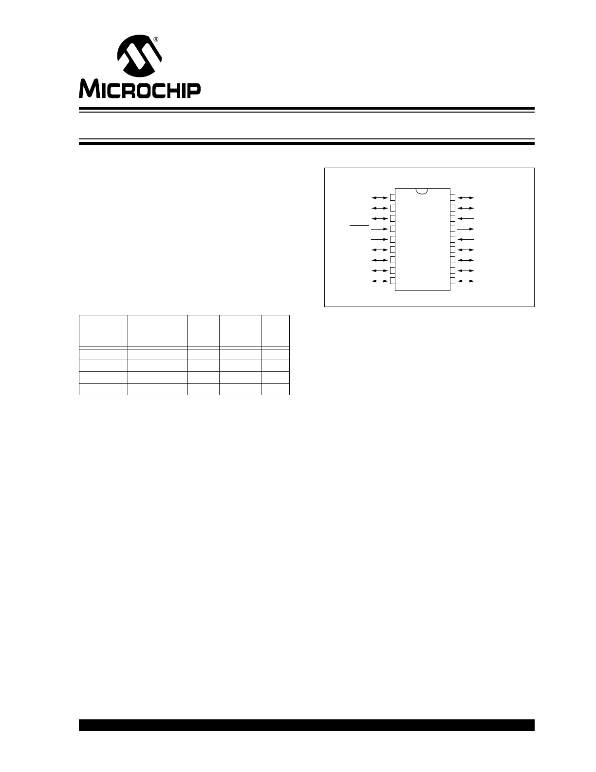
Pin Diagrams
Special Microcontroller Features:
• In-Circuit Serial Programming (ICSP™) - via two
pins (ROM devices support only Data EEPROM
programming)
• Power-on Reset (POR)
• Power-up Timer (PWRT)
• Oscillator Start-up Timer (OST)
• Watchdog Timer (WDT) with its own on-chip RC
oscillator for reliable operation
• Code-protection
• Power saving SLEEP mode
• Selectable oscillator options
CMOS Flash/EEPROM Technology:
• Low-power, high-speed technology
• Fully static design
• Wide operating voltage range:
- Commercial: 2.0V to 6.0V
- Industrial:
2.0V to 6.0V
• Low power consumption:
- < 2 mA typical @ 5V, 4 MHz
- 15
A typical @ 2V, 32 kHz
- < 1
A typical standby current @ 2V
Device
Program
Memory
(words)
Data
RAM
(bytes)
Data
EEPROM
(bytes)
Max.
Freq
(MHz)
PIC16F83
512 Flash
36
64
10
PIC16F84
1 K Flash
68
64
10
PIC16CR83
512 ROM
36
64
10
PIC16CR84
1 K ROM
68
64
10
RA1
RA0
OSC1/CLKIN
OSC2/CLKOUT
V
DD
RB7
RB6
RB5
RB4
RA2
RA3
RA4/T0CKI
MCLR
V
SS
RB0/INT
RB1
RB2
RB3
1
2
3
4
5
6
7
8
9
18
17
16
15
14
13
12
11
10
PDIP, SOIC
PIC
16F
8X
PIC1
6
CR8
X
PIC16F8X
18-pin Flash/EEPROM 8-Bit Microcontrollers

PIC16F8X
DS30430D-page 2
1996-2013 Microchip Technology Inc.
Table of Contents
1.0
General Description ...................................................................................................................................................................... 3
2.0
PIC16F8X Device Varieties .......................................................................................................................................................... 5
3.0
Architectural Overview .................................................................................................................................................................. 7
4.0
Memory Organization ................................................................................................................................................................. 11
5.0
I/O Ports...................................................................................................................................................................................... 21
6.0
Timer0 Module and TMR0 Register............................................................................................................................................ 27
7.0
Data EEPROM Memory.............................................................................................................................................................. 33
8.0
Special Features of the CPU ...................................................................................................................................................... 37
9.0
Instruction Set Summary ............................................................................................................................................................ 53
10.0 Development Support ................................................................................................................................................................. 69
11.0 Electrical Characteristics for PIC16F83 and PIC16F84 .............................................................................................................. 73
12.0 Electrical Characteristics for PIC16CR83 and PIC16CR84 ........................................................................................................ 85
13.0 DC & AC Characteristics Graphs/Tables.................................................................................................................................... 97
14.0 Packaging Information .............................................................................................................................................................. 109
Appendix A:
Feature Improvements - From PIC16C5X To PIC16F8X .......................................................................................... 113
Appendix B:
Code Compatibility - from PIC16C5X to PIC16F8X.................................................................................................. 113
Appendix C:
What’s New In This Data Sheet ................................................................................................................................. 114
Appendix D:
What’s Changed In This Data Sheet ......................................................................................................................... 114
Appendix E:
Conversion Considerations - PIC16C84 to PIC16F83/F84 And PIC16CR83/CR84.................................................. 115
Index ................................................................................................................................................................................................. 117
On-Line Support................................................................................................................................................................................. 119
Reader Response .............................................................................................................................................................................. 120
PIC16F8X Product Identification System ........................................................................................................................................... 121
Sales and Support.............................................................................................................................................................................. 121
To Our Valued Customers
We constantly strive to improve the quality of all our products and documentation. We have spent a great deal of
time to ensure that these documents are correct. However, we realize that we may have missed a few things. If you
find any information that is missing or appears in error, please use the reader response form in the back of this data
sheet to inform us. We appreciate your assistance in making this a better document.

PIC16F8X
1996-2013 Microchip Technology Inc.
DS30430D-page 3
1.0
GENERAL DESCRIPTION
The PIC16F8X is a group in the PIC16CXX family of
low-cost, high-performance, CMOS, fully-static, 8-bit
microcontrollers. This group contains the following
devices:
• PIC16F83
• PIC16F84
• PIC16CR83
• PIC16CR84
All PIC
®
microcontrollers employ an advanced RISC
architecture. PIC16F8X devices have enhanced core
features, eight-level deep stack, and multiple internal
and external interrupt sources. The separate
instruction and data buses of the Harvard architecture
allow a 14-bit wide instruction word with a separate
8-bit wide data bus. The two stage instruction pipeline
allows all instructions to execute in a single cycle,
except for program branches (which require two
cycles). A total of 35 instructions (reduced instruction
set) are available. Additionally, a large register set is
used to achieve a very high performance level.
PIC16F8X microcontrollers typically achieve a 2:1 code
compression and up to a 4:1 speed improvement (at 20
MHz) over other 8-bit microcontrollers in their class.
The PIC16F8X has up to 68 bytes of RAM, 64 bytes of
Data EEPROM memory, and 13 I/O pins. A timer/coun-
ter is also available.
The PIC16CXX family has special features to reduce
external components, thus reducing cost, enhancing
system reliability and reducing power consumption.
There are four oscillator options, of which the single pin
RC oscillator provides a low-cost solution, the LP
oscillator minimizes power consumption, XT is a
standard crystal, and the HS is for High Speed crystals.
The SLEEP (power-down) mode offers power saving.
The user can wake the chip from sleep through several
external and internal interrupts and resets.
A highly reliable Watchdog Timer with its own on-chip
RC oscillator provides protection against software lock-
up.
The devices with Flash program memory allow the
same device package to be used for prototyping and
production. In-circuit reprogrammability allows the
code to be updated without the device being removed
from the end application. This is useful in the
development of many applications where the device
may not be easily accessible, but the prototypes may
require code updates. This is also useful for remote
applications where the code may need to be updated
(such as rate information).
Table 1-1 lists the features of the PIC16F8X. A simpli-
fied block diagram of the PIC16F8X is shown in
Figure 3-1.
The PIC16F8X fits perfectly in applications ranging
from high speed automotive and appliance motor
control to low-power remote sensors, electronic locks,
security devices and smart cards. The Flash/EEPROM
technology makes customization of application
programs (transmitter codes, motor speeds, receiver
frequencies, security codes, etc.) extremely fast and
convenient. The small footprint packages make this
microcontroller series perfect for all applications with
space limitations. Low-cost, low-power, high
performance, ease-of-use and I/O flexibility make the
PIC16F8X very versatile even in areas where no
microcontroller use has been considered before
(e.g., timer functions; serial communication; capture,
compare and PWM functions; and co-processor
applications).
The serial in-system programming feature (via two
pins) offers flexibility of customizing the product after
complete assembly and testing. This feature can be
used to serialize a product, store calibration data, or
program the device with the current firmware before
shipping.
1.1
Family and Upward Compatibility
Those users familiar with the PIC16C5X family of
microcontrollers will realize that this is an enhanced
version of the PIC16C5X architecture. Please refer to
Appendix A for a detailed list of enhancements. Code
written for PIC16C5X devices can be easily ported to
PIC16F8X devices (Appendix B).
1.2
Development Support
The PIC16CXX family is supported by a full-featured
macro assembler, a software simulator, an in-circuit
emulator, a low-cost development programmer and a
full-featured programmer. A “C” compiler and fuzzy
logic support tools are also available.
PIC16F8X
DS30430D-page 4
1996-2013 Microchip Technology Inc.
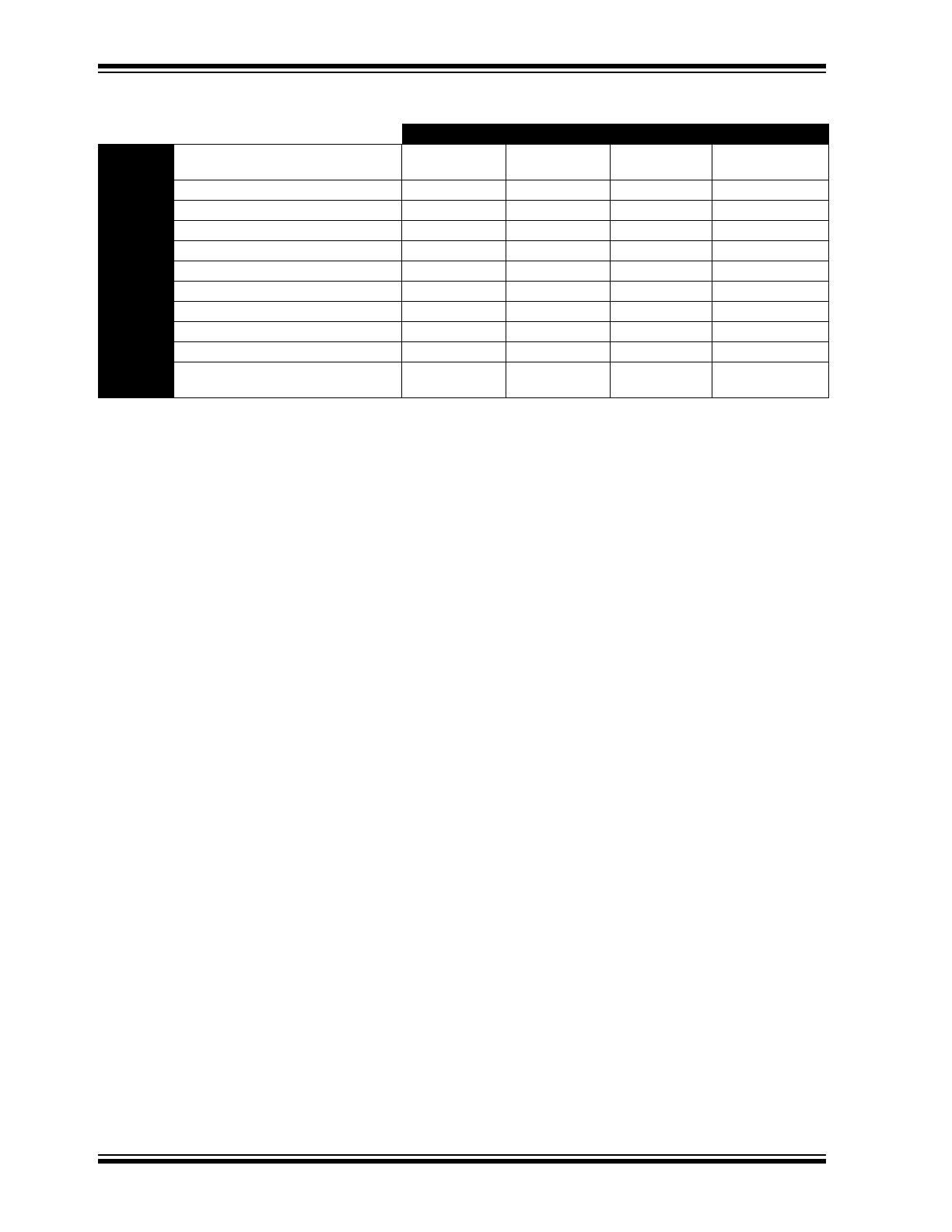
TABLE 1-1
PIC16F8X FAMILY OF DEVICES
PIC16F83
PIC16CR83
PIC16F84
PIC16CR84
Clock
Maximum Frequency
of Operation (MHz)
10
10
10
10
Flash Program Memory
512
—
1K
—
Memory
EEPROM Program Memory
—
—
—
—
ROM Program Memory
—
512
—
1K
Data Memory (bytes)
36
36
68
68
Data EEPROM (bytes)
64
64
64
64
Peripherals
Timer Module(s)
TMR0
TMR0
TMR0
TMR0
Features
Interrupt Sources
4
4
4
4
I/O Pins
13
13
13
13
Voltage Range (Volts)
2.0-6.0
2.0-6.0
2.0-6.0
2.0-6.0
Packages
18-pin DIP,
SOIC
18-pin DIP,
SOIC
18-pin DIP,
SOIC
18-pin DIP,
SOIC
All PIC
®
Family devices have Power-on Reset, selectable Watchdog Timer, selectable code protect and high I/O current capability.
All PIC16F8X Family devices use serial programming with clock pin RB6 and data pin RB7.

PIC16F8X
1996-2013 Microchip Technology Inc.
DS30430D-page 5
2.0
PIC16F8X DEVICE VARIETIES
A variety of frequency ranges and packaging options
are available. Depending on application and production
requirements the proper device option can be selected
using the information in this section. When placing
orders, please use the “PIC16F8X Product
Identification System” at the back of this data sheet to
specify the correct part number.
There are four device “types” as indicated in the device
number.
1.
F, as in PIC16F84. These devices have Flash
program memory and operate over the standard
voltage range.
2.
LF, as in PIC16LF84. These devices have Flash
program memory and operate over an extended
voltage range.
3.
CR, as in PIC16CR83. These devices have
ROM program memory and operate over the
standard voltage range.
4.
LCR, as in PIC16LCR84. These devices have
ROM program memory and operate over an
extended voltage range.
When discussing memory maps and other architectural
features, the use of F and CR also implies the LF and
LCR versions.
2.1
Flash Devices
These devices are offered in the lower cost plastic
package, even though the device can be erased and
reprogrammed. This allows the same device to be used
for prototype development and pilot programs as well
as production.
A further advantage of the electrically-erasable Flash
version is that it can be erased and reprogrammed in-
circuit, or by device programmers, such as Microchip's
PICSTART
®
Plus or PRO MATE
®
II programmers.
2.2
Quick-Turnaround-Production (QTP)
Devices
Microchip offers a QTP Programming Service for
factory production orders. This service is made
available for users who choose not to program a
medium to high quantity of units and whose code
patterns have stabilized. The devices have all Flash
locations and configuration options already pro-
grammed by the factory. Certain code and prototype
verification procedures do apply before production
shipments are available.
For information on submitting a QTP code, please
contact your Microchip Regional Sales Office.
2.3
Serialized Quick-Turnaround-
Production (SQTP
) Devices
Microchip offers the unique programming service
where a few user-defined locations in each device are
programmed with different serial numbers. The serial
numbers may be random, pseudo-random
or sequential.
Serial programming allows each device to have a
unique number which can serve as an entry-code,
password or ID number.
For information on submitting a SQTP code, please
contact your Microchip Regional Sales Office.
2.4
ROM Devices
Some of Microchip’s devices have a corresponding
device where the program memory is a ROM. These
devices give a cost savings over Microchip’s traditional
user programmed devices (EPROM, EEPROM).
ROM devices (PIC16CR8X) do not allow serialization
information in the program memory space. The user
may program this information into the Data EEPROM.
For information on submitting a ROM code, please
contact your Microchip Regional Sales Office.
SM

PIC16F8X
DS30430D-page 6
1996-2013 Microchip Technology Inc.
NOTES:

PIC16F8X
1996-2013 Microchip Technology Inc.
DS30430D-page 7
3.0
ARCHITECTURAL OVERVIEW
The high performance of the PIC16CXX family can be
attributed to a number of architectural features
commonly found in RISC microprocessors. To begin
with, the PIC16CXX uses a Harvard architecture. This
architecture has the program and data accessed from
separate memories. So the device has a program
memory bus and a data memory bus. This improves
bandwidth over traditional von Neumann architecture
where program and data are fetched from the same
memory (accesses over the same bus). Separating
program and data memory further allows instructions to
be sized differently than the 8-bit wide data word.
PIC16CXX opcodes are 14-bits wide, enabling single
word instructions. The full 14-bit wide program memory
bus fetches a 14-bit instruction in a single cycle. A two-
stage pipeline overlaps fetch and execution of instruc-
tions (Example 3-1). Consequently, all instructions exe-
cute in a single cycle except for program branches.
The PIC16F83 and PIC16CR83 address 512 x 14 of
program memory, and the PIC16F84 and PIC16CR84
address 1K x 14 program memory. All program mem-
ory is internal.
The PIC16CXX can directly or indirectly address its
register files or data memory. All special function
registers including the program counter are mapped in
the data memory. An orthogonal (symmetrical)
instruction set makes it possible to carry out any oper-
ation on any register using any addressing mode. This
symmetrical nature and lack of ‘special optimal
situations’ make programming with the PIC16CXX
simple yet efficient. In addition, the learning curve is
reduced significantly.
PIC16F8X
DS30430D-page 8
1996-2013 Microchip Technology Inc.
PIC16CXX devices contain an 8-bit ALU and working
register. The ALU is a general purpose arithmetic unit.
It performs arithmetic and Boolean functions between
data in the working register and any register file.
The ALU is 8-bits wide and capable of addition,
subtraction, shift and logical operations. Unless
otherwise mentioned, arithmetic operations are two's
complement in nature. In two-operand instructions,
typically one operand is the working register
(W register), and the other operand is a file register or
an immediate constant. In single operand instructions,
the operand is either the W register or a file register.
The W register is an 8-bit working register used for ALU
operations. It is not an addressable register.
Depending on the instruction executed, the ALU may
affect the values of the Carry (C), Digit Carry (DC), and
Zero (Z) bits in the STATUS register. The C and DC bits
operate as a borrow and digit borrow out bit,
respectively, in subtraction. See the SUBLW and SUBWF
instructions for examples.
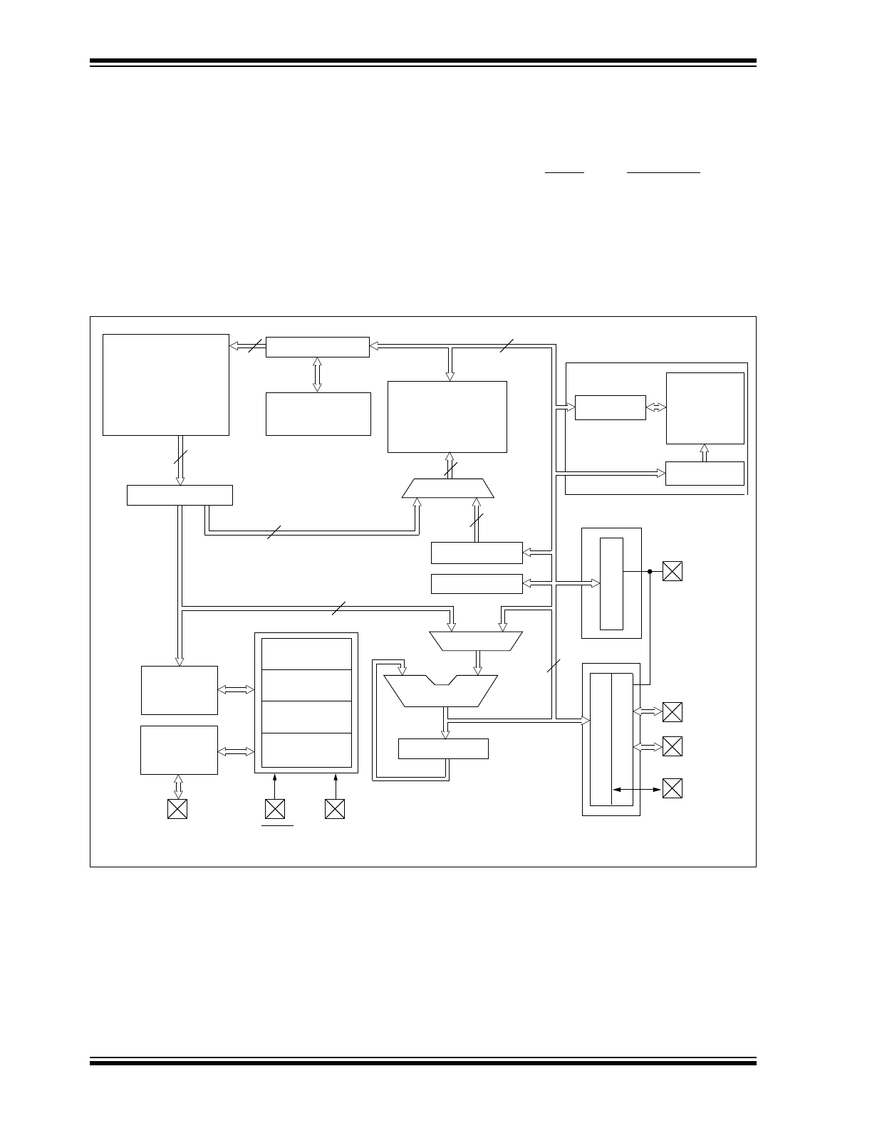
A simplified block diagram for the PIC16F8X is shown
in Figure 3-1, its corresponding pin description is
shown in Table 3-1.
FIGURE 3-1:
PIC16F8X BLOCK DIAGRAM
Flash/ROM
Program
Memory
Program Counter
13
Program
Bus
Instruction reg
8 Level Stack
(13-bit)
Direct Addr
8
Instruction
Decode &
Control
Timing
Generation
OSC2/CLKOUT
OSC1/CLKIN
Power-up
Timer
Oscillator
Start-up Timer
Power-on
Reset
Watchdog
Timer
MCLR
V
DD
, V
SS
W reg
ALU
MUX
I/O Ports
TMR0
STATUS reg
FSR reg
Indirect
Addr
RA3:RA0
RB7:RB1
RA4/T0CKI
EEADR
EEPROM
Data Memory
64 x 8
EEDATA
Addr Mux
RAM Addr
RAM
File Registers
EEPROM Data Memory
Data Bus
5
7
7
PIC16F84/CR84
1K x 14
PIC16F83/CR83
512 x 14
PIC16F83/CR83
36 x 8
PIC16F84/CR84
68 x 8
RB0/INT
14
8
8
PIC16F8X
1996-2013 Microchip Technology Inc.
DS30430D-page 9
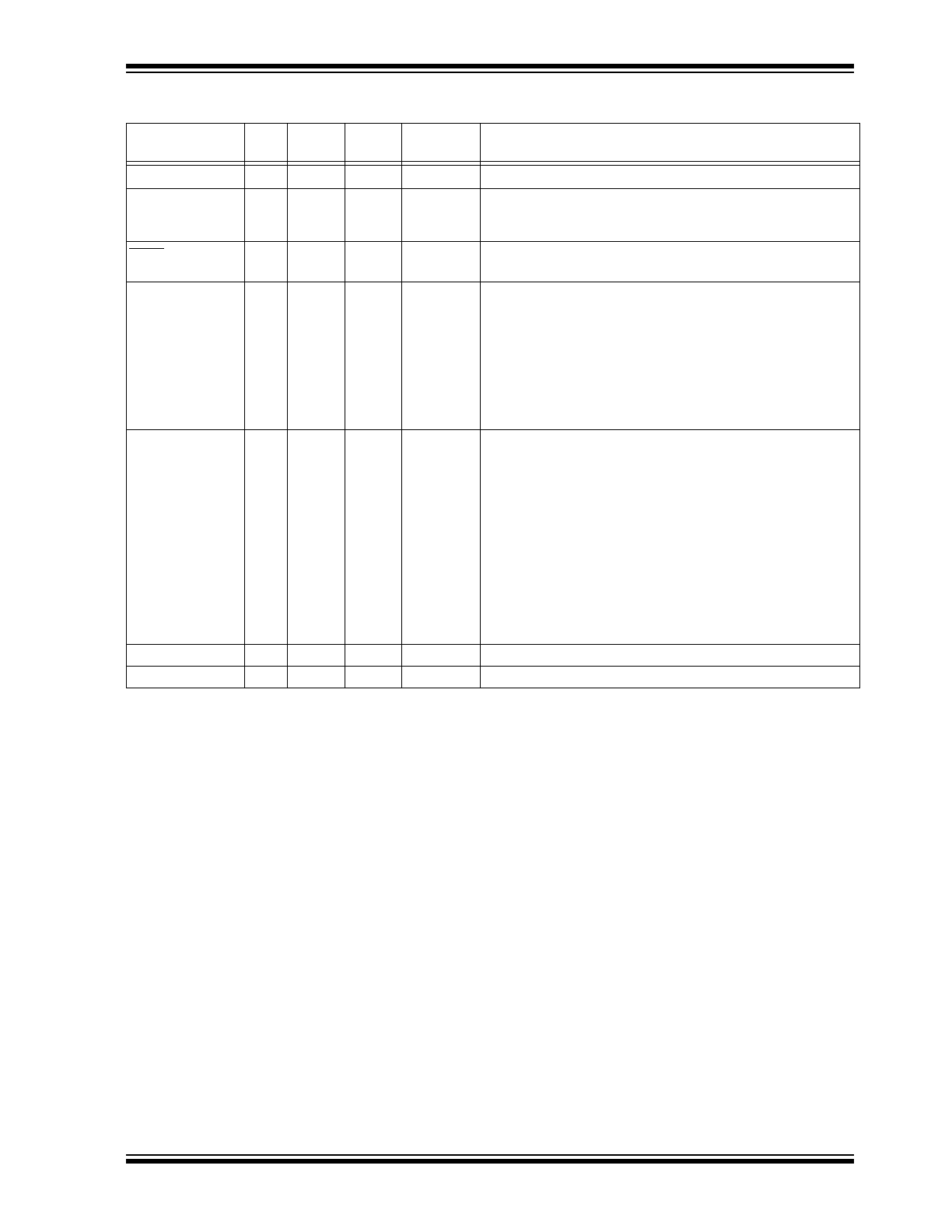
TABLE 3-1
PIC16F8X PINOUT DESCRIPTION
Pin Name
DIP
No.
SOIC
No.
I/O/P
Type
Buffer
Type
Description
OSC1/CLKIN
16
16
I
ST/CMOS
(3)
Oscillator crystal input/external clock source input.
OSC2/CLKOUT
15
15
O
—
Oscillator crystal output. Connects to crystal or resonator in crystal
oscillator mode. In RC mode, OSC2 pin outputs CLKOUT which has
1/4 the frequency of OSC1, and denotes the instruction cycle rate.
MCLR
4
4
I/P
ST
Master clear (reset) input/programming voltage input. This pin is an
active low reset to the device.
PORTA is a bi-directional I/O port.
RA0
17
17
I/O
TTL
RA1
18
18
I/O
TTL
RA2
1
1
I/O
TTL
RA3
2
2
I/O
TTL
RA4/T0CKI
3
3
I/O
ST
Can also be selected to be the clock input to the TMR0 timer/
counter. Output is open drain type.
PORTB is a bi-directional I/O port. PORTB can be software pro-
grammed for internal weak pull-up on all inputs.
RB0/INT
6
6
I/O
TTL/ST
(1)
RB0/INT can also be selected as an external interrupt pin.
RB1
7
7
I/O
TTL
RB2
8
8
I/O
TTL
RB3
9
9
I/O
TTL
RB4
10
10
I/O
TTL
Interrupt on change pin.
RB5
11
11
I/O
TTL
Interrupt on change pin.
RB6
12
12
I/O
TTL/ST
(2)
Interrupt on change pin. Serial programming clock.
RB7
13
13
I/O
TTL/ST
(2)
Interrupt on change pin. Serial programming data.
V
SS
5
5
P
—
Ground reference for logic and I/O pins.
V
DD
14
14
P
—
Positive supply for logic and I/O pins.
Legend: I= input
O = output
I/O = Input/Output
P = power
— = Not used
TTL = TTL input
ST = Schmitt Trigger input
Note 1:
This buffer is a Schmitt Trigger input when configured as the external interrupt.
2:
This buffer is a Schmitt Trigger input when used in serial programming mode.
3:
This buffer is a Schmitt Trigger input when configured in RC oscillator mode and a CMOS input otherwise.
PIC16F8X
DS30430D-page 10
1996-2013 Microchip Technology Inc.
3.1
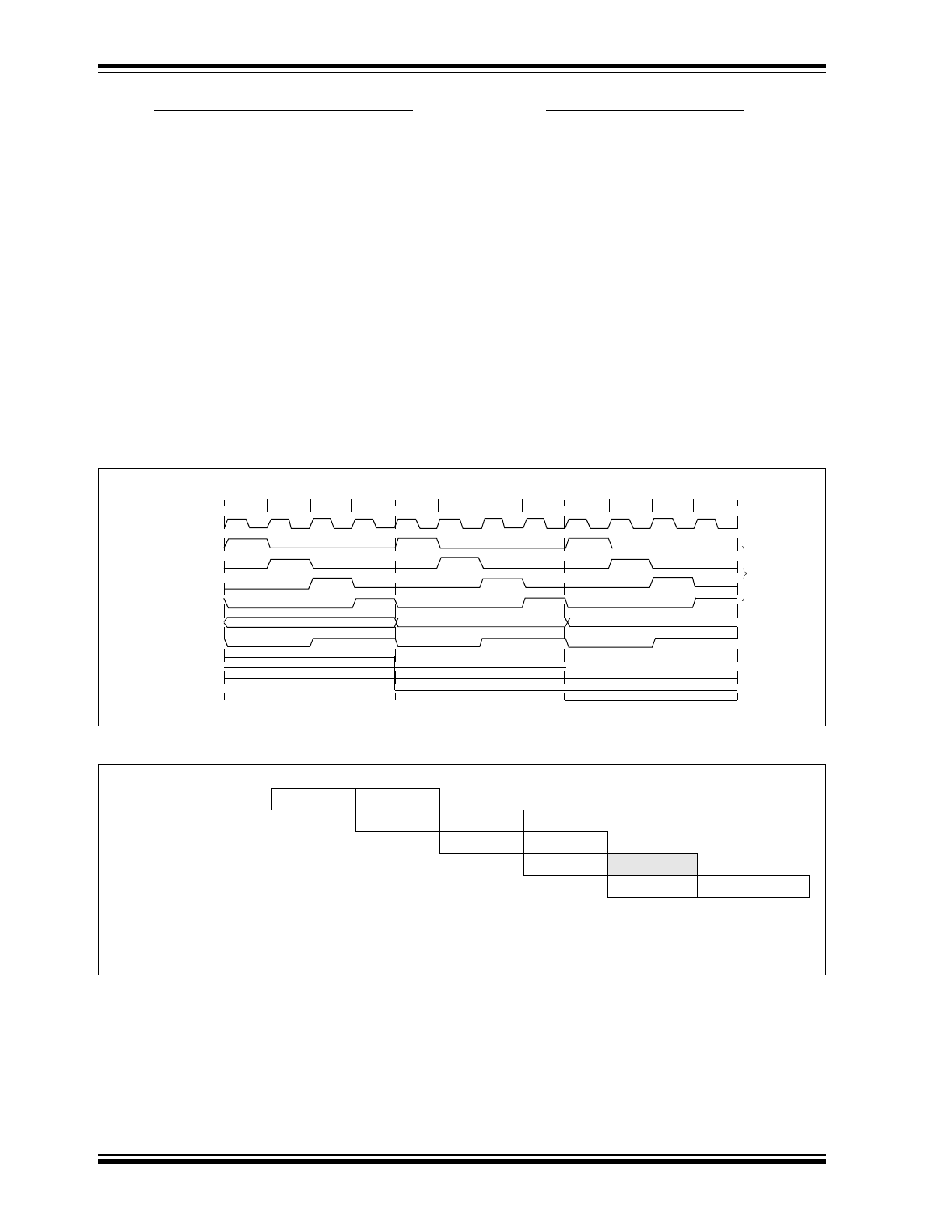
Clocking Scheme/Instruction Cycle
The clock input (from OSC1) is internally divided by
four to generate four non-overlapping quadrature
clocks namely Q1, Q2, Q3 and Q4. Internally, the
program counter (PC) is incremented every Q1, the
instruction is fetched from the program memory and
latched into the instruction register in Q4. The
instruction is decoded and executed during the
following Q1 through Q4. The clocks and instruction
execution flow is shown in Figure 3-2.
3.2
Instruction Flow/Pipelining
An “Instruction Cycle” consists of four Q cycles (Q1,
Q2, Q3 and Q4). The instruction fetch and execute are
pipelined such that fetch takes one instruction cycle
while decode and execute takes another instruction
cycle. However, due to the pipelining, each instruction
effectively executes in one cycle. If an instruction
causes the program counter to change (e.g., GOTO)
then two cycles are required to complete the instruction
(Example 3-1).
A fetch cycle begins with the Program Counter (PC)
incrementing in Q1.
In the execution cycle, the fetched instruction is latched
into the “Instruction Register” in cycle Q1. This
instruction is then decoded and executed during the
Q2, Q3, and Q4 cycles. Data memory is read during Q2
(operand read) and written during Q4 (destination
write).
FIGURE 3-2:
CLOCK/INSTRUCTION CYCLE
EXAMPLE 3-1:
INSTRUCTION PIPELINE FLOW
Q1
Q2
Q3
Q4
Q1
Q2
Q3
Q4
Q1
Q2
Q3
Q4
OSC1
Q1
Q2
Q3
Q4
PC
OSC2/CLKOUT
(RC mode)
PC
PC+1
PC+2
Fetch INST (PC)
Execute INST (PC-1)
Fetch INST (PC+1)
Execute INST (PC)
Fetch INST (PC+2)
Execute INST (PC+1)
Internal
phase
clock
All instructions are single cycle, except for any program branches. These take two cycles since the fetch
instruction is “flushed” from the pipeline while the new instruction is being fetched and then executed.
1. MOVLW 55h
Fetch 1
Execute 1
2. MOVWF PORTB
Fetch 2
Execute 2
3. CALL SUB_1
Fetch 3
Execute 3
4. BSF PORTA, BIT3
Fetch 4
Flush
Fetch SUB_1 Execute SUB_1