
1996 Microchip Technology Inc.
DS30139I-page 1
This document includes the programming
specifications for the following devices:
1.0
PROGRAMMING THE PIC17CXX
The PIC17CXX is programmed using the TABLWT
instruction. The table pointer points to the internal
EPROM location start. Therefore, a user can program
an EPROM location while executing code (even from
internal EPROM). This programming specification
applies to PIC17CXX devices in all packages.
For the convenience of a programmer developer, a
“program & verify” routine is provided in the on-chip test
program memory space, the program resides in ROM
and not EPROM. Therefore, it is not erasable. The
“program/verify” routine allows the user to load any
address, program a location, verify a location or incre-
ment to the next location. It allows variable program-
ming pulse width.
1.1
Hardware Requirements
Since the PIC17CXX under programming is actually
executing code from “boot ROM,” a clock must be pro-
vided to the part. Furthermore, the PIC17CXX under
programming may have any oscillator configuration
(EC, XT, LF or RC). Therefore, the external clock driver
must be able to overdrive pulldown in RC mode. CMOS
drivers are required since the OSC1 input has a
Schmitt trigger input with levels (typically) of 0.2V
DD
and 0.8V
DD
. See the PIC17C4X data sheet
(DS30412A) for exact specifications.
• PIC17C42
• PIC17C42A
• PIC17CR42
• PIC17C43
• PIC17CR43
• PIC17C44
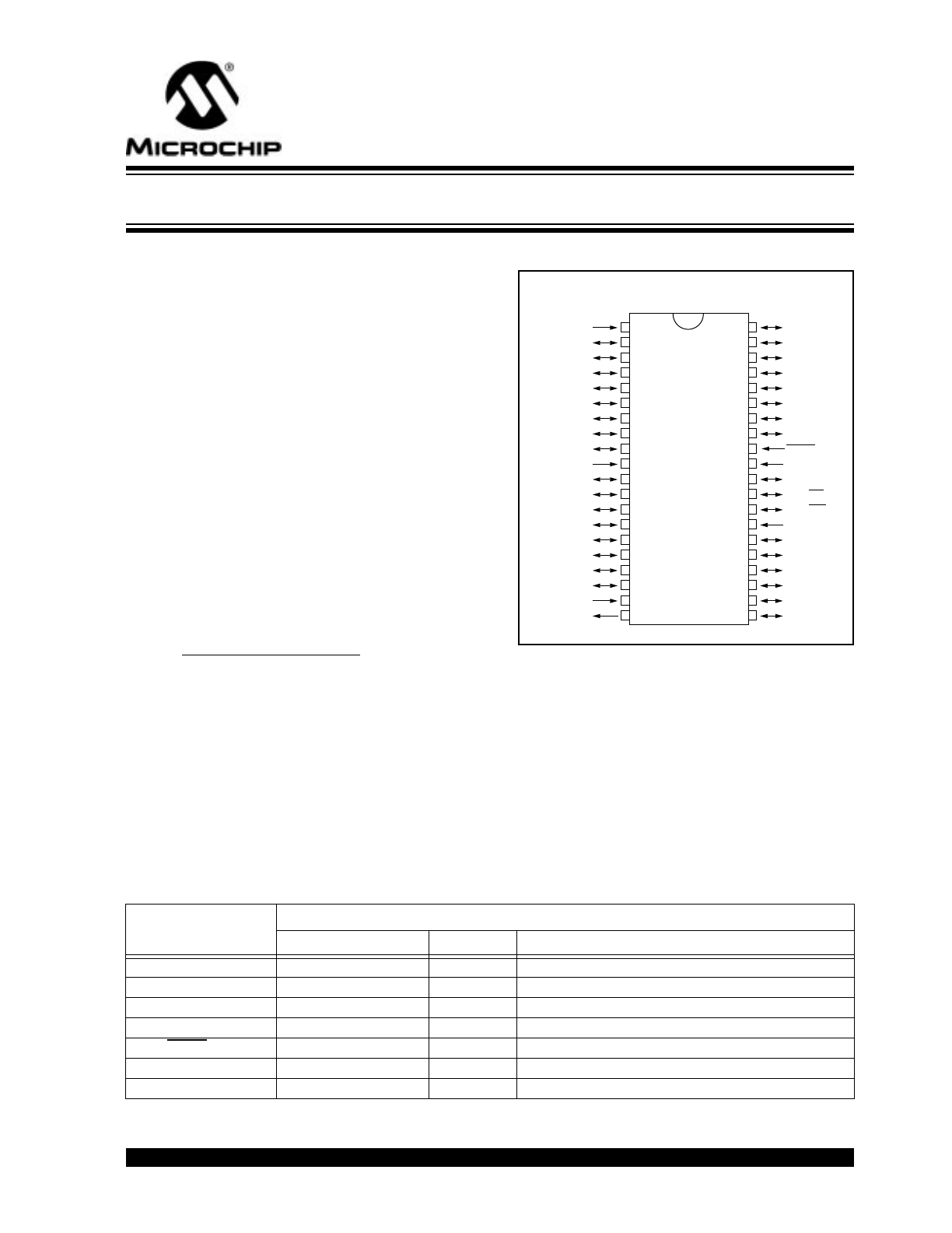
Pin Diagram
The PIC17CXX requires two programmable power
supplies, one for V
DD
(2.5V to 6.0V recommended) and
one for V
PP
(13
±
0.25V). Both supplies should have a
minimum resolution of 0.25V.
The PIC17CXX uses an intelligent algorithm. The algo-
rithm calls for program verification at V
DD
min as well as
V
DD
max. Verification at V
DD
min guarantees good
“erase margin”. Verification at V
DD
max guarantees
good “program margin”. Three times (3X) additional
pulses will increase program margin then beyond V
DD
(max.) and insure safe operation in user system.
RC1/AD1
RD0/AD8
RD1/AD9
RD2/AD10
RD3/AD11
RD4/AD12
RD5/AD13
RD6/AD14
RD7/AD15
MCLR/V
PP
V
SS
RE0/ALE
RE1/OE
RE2/WR
TEST
RA0/INT
RA1/T0CKI
RA2
RA3
RA4/RX/DT
RA5/TX/CK
V
DD
RC0/AD0
RC2/AD2
RC3/AD3
RC4/AD4
RC5/AD5
RC6/AD6
RC7/AD7
V
SS
RB0/CAP1
RB1/CAP2
RB2/PWM1
RB3/PWM2
RB4/TCLK12
RB5/TCLK3
RB6
RB7
OSC1/CLKIN
OSC2/CLKOUT
1
2
3
4
5
6
7
8
9
10
11
12
13
14
15
16
17
18
19
20
40
39
38
37
36
35
34
33
32
31
30
29
28
27
26
25
24
23
22
21
PIC17CXX
40L PDIP, Windowed CERDIP
PIC17CXX
EPROM Memory Programming Specification
PIN DESCRIPTIONS (DURING PROGRAMMING): PIC17C42/42A/43/44
Pin Name
During Programming
Pin Name
Pin Type
Pin Description
RA <0:4>
RA <0:4>
I
Necessary in programming mode
TEST
TEST
I
Must be set to “high” to enter programming mode
RB <7:0>
PAD <15:8>
I/O
Address & data: high byte
RC <7:0>
PAD <7:0>
I/O
Address & data: low byte
MCLR/V
PP
V
PP
P
Programming Power
V
DD
V
DD
P
Power Supply
V
SS
V
SS
P
Ground
Legend: I = Input, O = Output, P = Power
This document was created with FrameMaker 4 0 4
PIC17CXX
DS30139I-page 2
1996 Microchip Technology Inc.
The actual programming must be done with V
DD
in the
V
DDP
range (4.75 - 5.25V).
V
DDP
=V
DD
range required during programming.
V
DD
min.=minimum operating V
DD
spec for the part.
V
DD
max.=maximum operating V
CC
spec for the part.
Programmers must verify the PIC17CXX at its speci-
fied V
DD
max and V
DD
min levels. Since Microchip may
introduce future versions of the PIC17CXX with a
broader V
DD
range, it is best that these levels are user
selectable (defaults are ok).
2.0
PROGRAM MODE ENTRY
To execute the programming routine, the user must
hold TEST pin high, RA2, RA3 must be low and RA4
must be high (after power-up) while keeping MCLR low
and then raise MCLR pin from V
IL
to V
DD
or V
PP
. This
will force FFE0h in the program counter and execution
will begin at that location (the beginning of the boot
code) following reset. Execution is forced to Internal
mode by overriding the fuse configuration. The code
protect bit is not overwritten. The program immediately
polls PORT RB<7:0> to determine a branch address.
Presenting E1h on PORT RB will cause the program to
jump to and execute the “program/verify” routine.
Note:
Any programmer not meeting these
requirements may only be classified as
"prototype" or "development" programmer
but not a "production" quality programmer.
All unused pins during programming are in high imped-
ance state.
PORTB (RB) has internal weak pull-ups which are
active during the programming mode. When TEST pin
is high, Power-up timer (PWRT) and Oscillator Start-up
Timers (OST) are disabled.
2.1
Program/Verify Mode
The program/verify mode is intended for full-feature
programmers. This mode offers the following capabili-
ties:
a)
Load any arbitrary 16-bit address to start pro-
gram and/or verify at that location.
b)
Increment address to program/verify the next
location.
c)
Allows arbitrary length programming pulse width.
d)
Following a “verify” allows option to program the
same location or increment and verify the next
location.
e)
Following a “program” allows options to program
the same location again, verify the same loca-
tion or to increment and verify the next location.
Note:
The OSC must not have 72 osc clocks
while the device MCLR is between V
IL
and
V
IHH
.
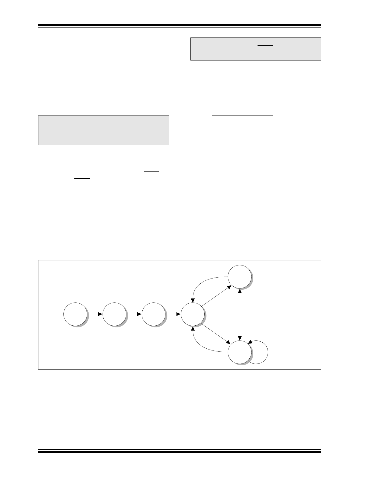
FIGURE 2-1:
PROGRAMMING/VERIFY STATE DIAGRAM
Increment
Address
Program
Verify
Pulse RA1
(Raise RA1
after RA0
↓
)
Pulse RA0
(RA0 pulse
width is
programming time)
Pulse
RA1
Pulse
RA1
RA0
↑
Raise RA1
before RA0
↓
Load
Address
Jump to
Program
Routine
Reset
Pulse
RA1
1996 Microchip Technology Inc.
DS30139I-page 3
EPROM Memory Programming Specification
2.1.1
LOADING NEW ADDRESS
The program allows new address to be loaded right out
of reset. A 16-bit address is presented on ports RB
(high byte) and RC (low byte) and the RA1 is pulsed
(0
→
1, then 1
→
0). The address is latched on the ris-
ing edge of RA1. See timing diagrams for details. After
loading an address, the program automatically goes
into a “verify cycle”. To load a new address at any time,
the PIC17C4X must be reset and the programming
mode re-entered.
2.1.2
VERIFY (OR READ) MODE
“Verify mode” can be entered from “Load address”
mode, “program mode” or “verify mode”. In verify mode
pulsing RA1 will turn on PORTS RB and RC output
drivers and output the 16-bit value from the current
location. Pulsing RA1 again will increment location
count and be ready for the next verify cycle. Pulsing
RA0 will begin a program cycle.
2.1.3
PROGRAM CYCLE
“Program cycle” is entered from “verify cycle” or pro-
gram cycle” itself. After a verify, pulsing RA0 will begin
a program cycle. 16-bit data must be presented on
PORTS RB (high byte) and RC (low byte) before RA0
is raised.
The data is sampled 3 T
CY
cycles after the rising edge
of RA0. Programming continues for the duration of RA0
pulse.
At the end of programming the user can choose one of
three different routes. If RA1 is kept low and RA0 is
pulsed again, the same location will be programmed
again. This is useful for applying over programming
pulses. If RA1 is raised before RA0 falling edge, then a
verify cycle is started without address increment. Rais-
ing RA1 after RA0 goes low will increment address and
begin verify cycle on the next address.
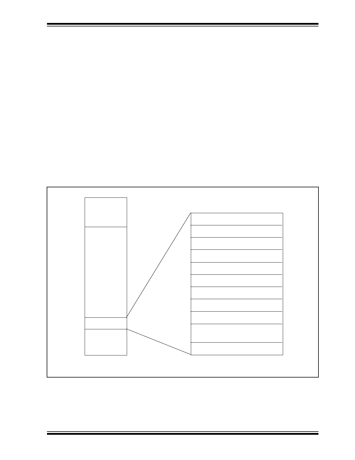
FIGURE 2-2:
PIC17C4X PROGRAM MEMORY MAP
On chip
Program
EPROM
Configuration
Word
FOSC0
FOSC1
WDTPS0
WDTPS1
PM0
PM1
PM2*
Reserved
Reserved
Reserved
FE00
FE01
FE02
FE03
FE04
FE05
FE06
FE07
FE08
FE09
FE0F
Reserved
0000
07FF
FE00
FE0F
FFFF
*This location does not exist for PIC17C42
PIC17CXX
DS30139I-page 4
1996 Microchip Technology Inc.
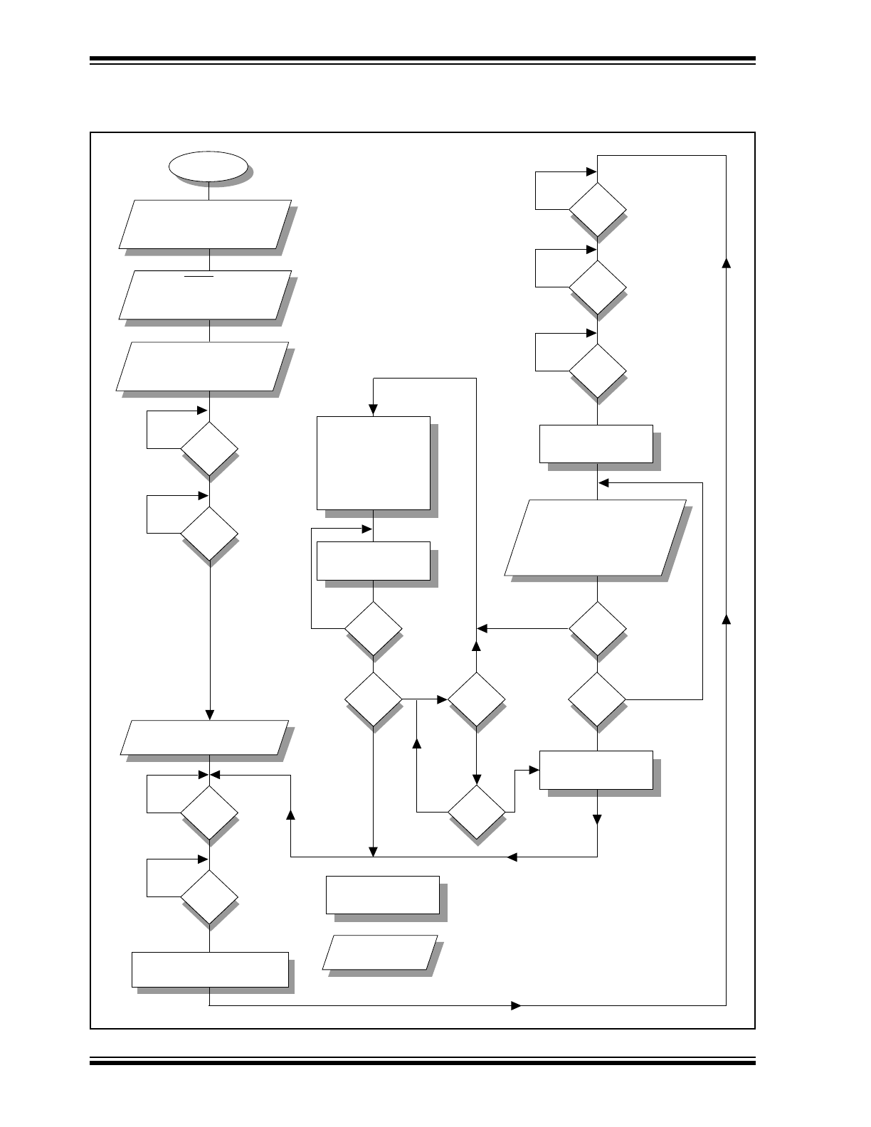
3.0
PROGRAMMING SPECIFICATIONS
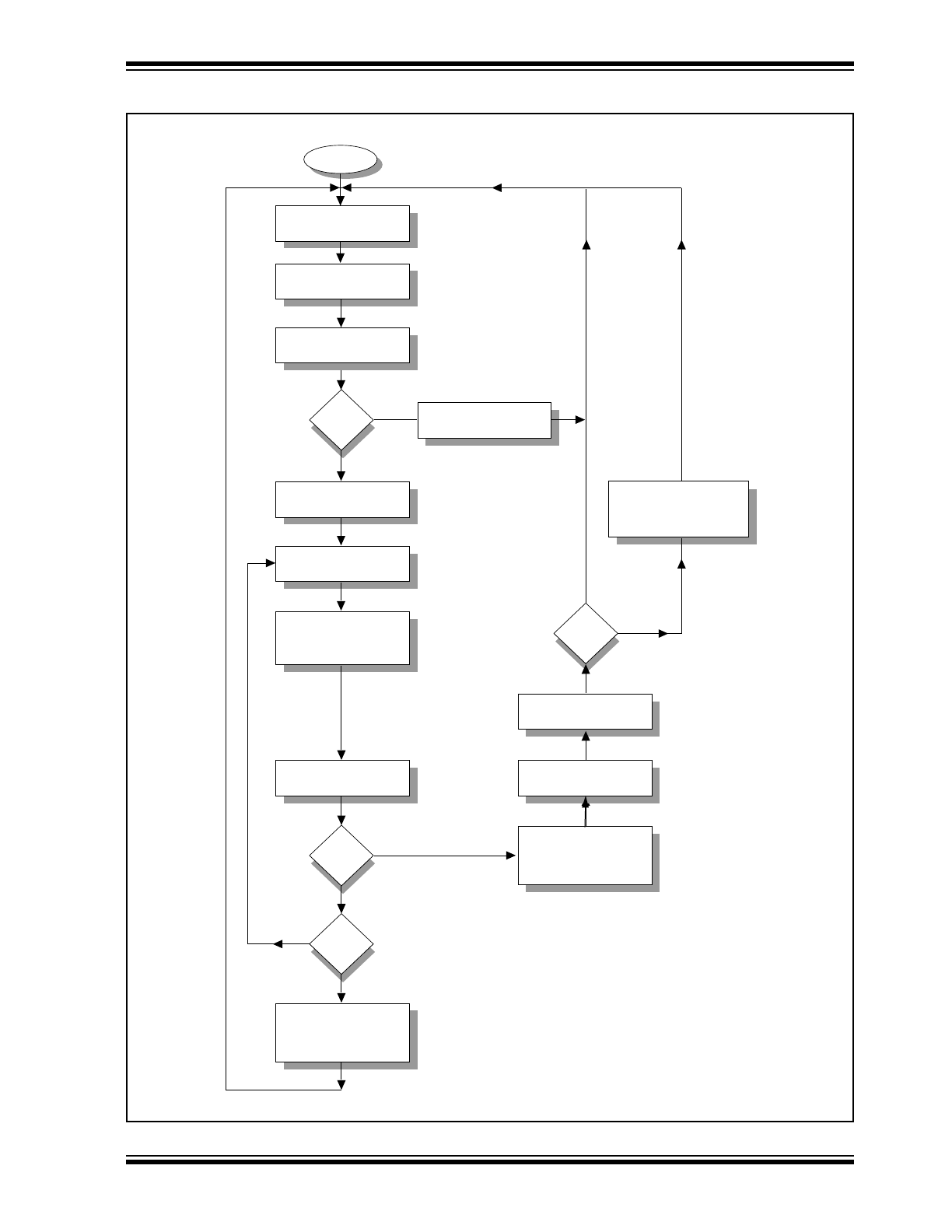
FIGURE 3-1:
PROGRAMMING ROUTINE FLOWCHART
If programming is desired,
force port B = MSB of data
force port C = LSB of data
(hold 10Tcyc after
RA0 is raised)
Present address on ports
RB, RC hold Tcy
after RA1 changes to 1
Reset
RA2 = 0
RA3 = 0
RA4 = 1
MCLR = 1
B port = 0xE1
(hold for 10 Tcy)
RA1
= 0
No
RA1
= 1
Yes
Stop driving address
on port
RA1
= 0
No
RA1
= 1
No
Yes
Yes
B port = MSB of Data
C port = LSB of Data
Read MSB of data
from port-B.
Read LSB of data
from port-C.
Enable RA0 to end
prog cycle
RA0 = 0
No
RA1
= 0
Yes
Yes
No
RA0= 1
RA1
= 1
No
No
Yes
RA0= 1
RA1
= 1
Yes
Yes
No
No
Yes
RA1
= 0
No
Yes
RA1
= 1
No
Yes
RA1
= 0
No
Yes
- B port is forced by the part
B port = xxx
- B port is tri-state, should be forced by user
Min RA1 high or low = 10 Tcy
Yes
No
B port = xxx
Increment
Address
Program 16 bit
data
B & C ports not
driven by part
1996 Microchip Technology Inc.
DS30139I-page 5
EPROM Memory Programming Specification
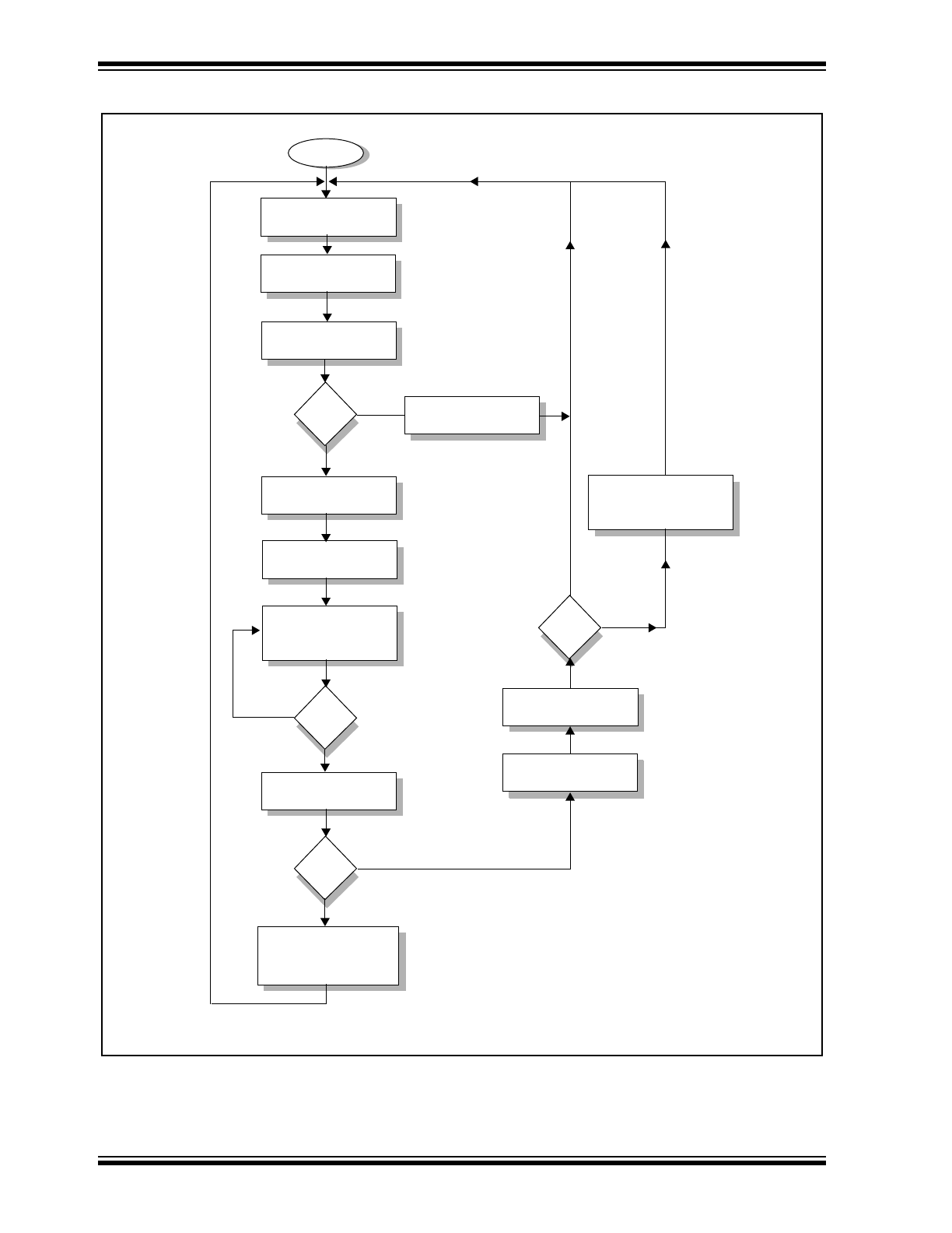
FIGURE 3-2:
RECOMMENDED PROGRAMMING ALGORITHM FOR USER EPROM
Start
Pass
Blank
check?
Yes
Yes
No
No
Pass?
Pulse-
count
>25
No
Apply (3 x Pulse-count)
more 100 µs programming
pulses for margin
(Over programming)
Load new address
Pulse-count = 0
Pass?
No
Yes
Verify blank
Issue "Blank check fail"
error message
Load new data
Set V
DD
= V
DDP
Verify location for
correct data
Program using 100µs
pulse increment
pulse-count
Location fails
programming, issue error
message "Unable to
program location"
Set V
DD
= V
DD
min
Verify location
Programming error:
Issue error message
"Fail verify @ V
DD
min/max"
Set V
DD
= V
DD
min
Set V
DD
= V
DD
max.
Verify location(s)
Set V
DD
= V
DD
max
Set V
DD
= V
DD
min
Set V
DD
= V
DD
min
“Fail verify @ V
DD
min/max”
PIC17CXX
DS30139I-page 6
1996 Microchip Technology Inc.
FIGURE 3-3:
RECOMMENDED PROGRAMMING ALGORITHM FOR CONFIGURATION WORDS
Load new address
Pulse-count = 0
Set V
DD
= V
DD
min
Verify blank
Issue “blank check fail”
Load new data
Set V
DD
= V
DDP
Set V
DD
= V
DD
max
Set V
DD
= V
DD
min
Verify location for
Program using 100
µ
s
Location fails
Programming error:
No
Yes
No
No
Yes
Yes
Start
Pass
Blank
check?
pulse increment
pulse-count
Pass?
Issue error message
“Fail verify @ V
DD
min/max”
Verify location(s)
Pass?
No
Yes
Pulse
count
<100
programming, issue error
message “Unable to
program location”
correct data
error message
Set V
DD
= V
DD
min
Set V
DD
= V
DD
min
Verify location
1996 Microchip Technology Inc.
DS30139I-page 7
EPROM Memory Programming Specification
4.0
CONFIGURATION WORD
Configuration bits are mapped into program memory.
Each bit is assigned one memory location. In erased
condition a bit will read as '1'. To program a bit, the user
needs to write to the memory address. The data is
immaterial; the very act of writing will program the bit.
The configuration word locations are shown in
Table 4-3.
The programmer should not program the
reserved locations to avoid unpredictable results
and to be compatible with future variations of the
PIC17C4X
.
It is also mandatory that configuration
locations are programmed in the strict order start-
ing from the first location (0xFE00) and ending with
the last (0xFE0F). Unpredictable results may occur
if the sequence is violated.
4.1
Reading Configuration Word
The PIC17CXX has seven configuration locations (see
Table 4-1). These locations can be programmed (read
as '0') or left unprogrammed (read as '1') to select var-
ious device configurations. Any write to a configuration
location, regardless of the data, will program that con-
figuration bit. Reading any configuration location
between 0xFE00 and 0xFE07 will place the low byte of
the configuration word (see Table 4-2) into PAD<7:0>
(PORTC). PAD<15:8> (PORTB) will be set to 0xFF.
Reading a configuration location between 0xFE08 and
0xFE0F will place the high byte of the configuration
word into PAD<7:0> (PORTC). PAD<15:8> (PORTB)
will be set to 0xFF.
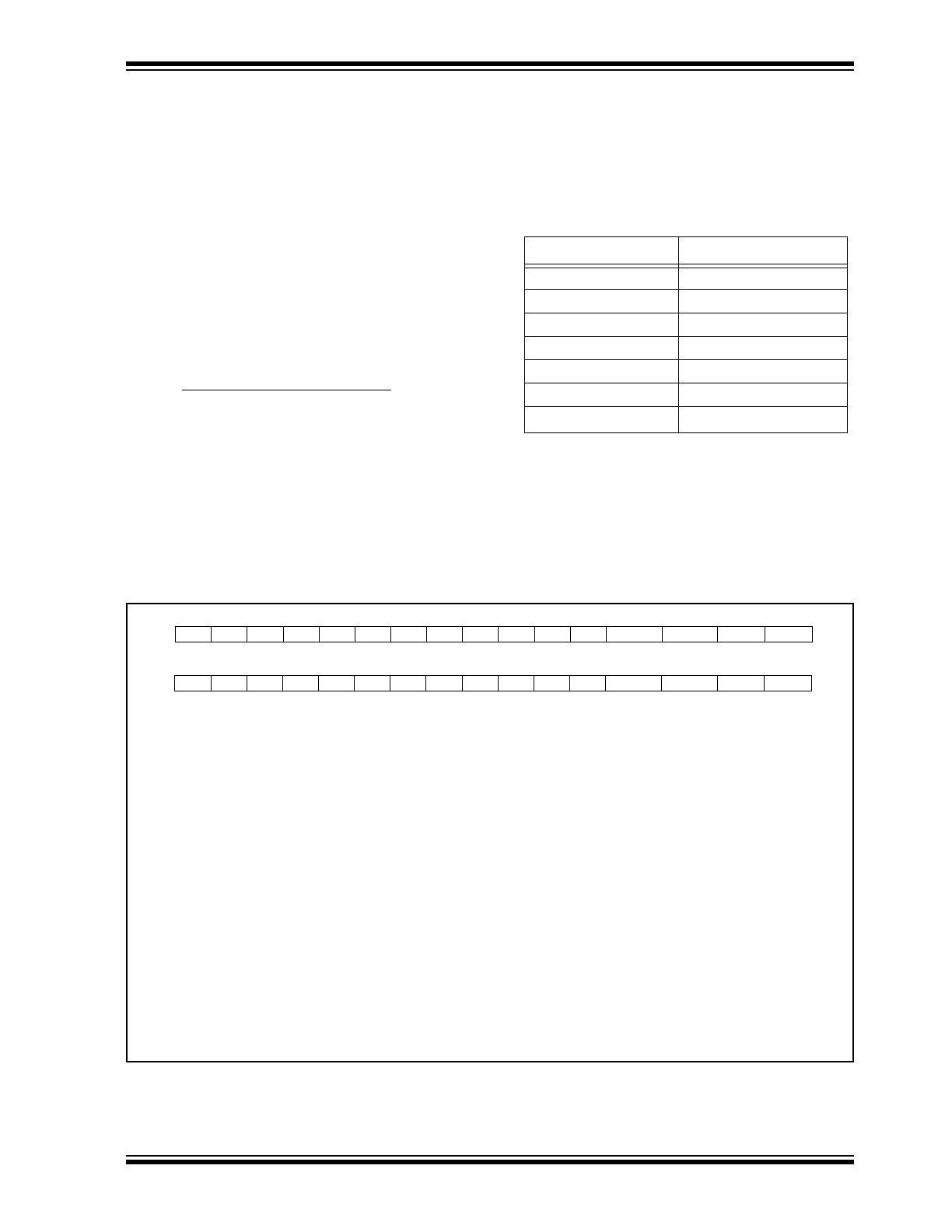
TABLE 4-1:
CONFIGURATION BIT
PROGRAMMING LOCATIONS
†
This location does not exist on the PIC17C42.
Bit
Address
FOSC0
0xFE00
FOSC1
0xFE01
WDTPS0
0xFE02
WDTPS1
0xFE03
PM0
0xFE04
PM1
0xFE06
PM2
†
0xFE0F
TABLE 4-2:
READ MAPPING OF CONFIGURATION BITS
—=Unused
PM<2:0>, Processor Mode Select bits
111 = Microprocessor mode
110 = Microcontroller mode
101 = Extended Microcontroller mode
000 = Code protected microcontroller mode
WDTPS<1:0>, WDT Prescaler Select bits.
11 = WDT enabled, postscaler = 0
10 = WDT enabled, postscaler = 256
01 = WDT enabled, postscaler = 64
00 = WDT disabled, 16-bit overflow timer
FOSC<1:0>, Oscillator Select bits
11
= EC oscillator
10 = XT oscillator
01 = RC oscillator
00 = LF oscillator
*
This bit does not exist on PIC17C42.
WDTPS1
FOSC1 FOSC0
WDTPS0
PM0
PM1
—
—
PM2*
1
1
1
1
1
1
1
1
1
1
1
1
1
1
1
1
—
—
—
8
9
10
11
12
13
14
15
0
1
2
3
4
5
6
7
—
—
—
8
9
10
11
12
13
14
15
0
1
2
3
4
5
6
7
—
PIC17CXX
DS30139I-page 8
1996 Microchip Technology Inc.
4.2
Embedding Configuration Word Information in the Hex File
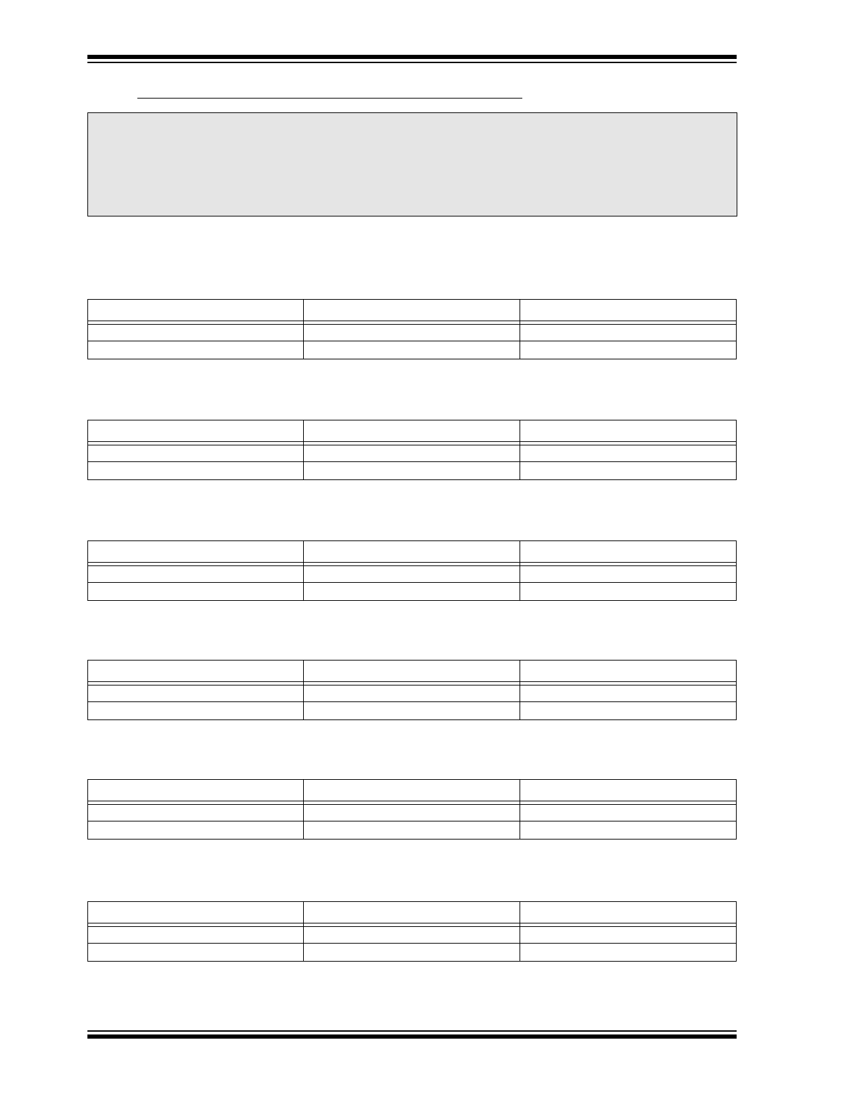
TABLE 4-3:
CONFIGURATION WORD
PIC17C42
To code protect:
• Protect all memory
XXXXXXXXX0X0XXXX
PIC17C42A
To code protect:
• Protect all memory
0XXXXXXXX0X0XXXX
PIC17CR42
To code protect:
• Protect all memory
0XXXXXXX0X0XXXX
PIC17C43
To code protect:
• Protect all memory
0XXXXXXX0X0XXXX
PIC17CR43
To code protect:
• Protect all memory
0XXXXXXX0X0XXXX
PIC17C44
To code protect:
• Protect all memory
0XXXXXXX0X0XXXX
Legend: X = Don’t care
*Write to on-chip EPROM memory is disabled. The only way these locations can be programmed is if a TABLWT
instruction is issued from an “on-chip” program memory space to program an on-chip memory location.
To allow portability of code, a PIC17C4X programmer is required to read the configuration word locations from the hex
file when loading the hex file. If configuration word information was not present in the hex file then a simple warning
message may be issued. Similarly, while saving a hex file, all configuration word information must be included. An
option to not include the configuration word information may be provided. When embedding configuration word infor-
mation in the hex file, it should be to address FE00h.
Microchip Technology Inc. feels strongly that this feature is important for the benefit of the end customer.
Program Memory Segment
R/W in Protected Mode
R/W in Unprotected Mode
Configuration Word (0xFE00)
Read Scrambled, Write Enabled
Read Unscrambled, Write Enabled
All memory
Read Scrambled, Write Disabled*
Read Unscrambled, Write Enabled
Program Memory Segment
R/W in Protected Mode
R/W in Unprotected Mode
Configuration Word (0xFE00)
Read Scrambled, Write Enabled
Read Unscrambled, Write Enabled
All memory
Read Scrambled, Write Disabled*
Read Unscrambled, Write Enabled
Program Memory Segment
R/W in Protected Mode
R/W in Unprotected Mode
Configuration Word (0xFE00)
Read Scrambled, Write Enabled
Read Unscrambled, Write Enabled
All memory
Read Scrambled, Write Disabled*
Read Unscrambled, Write Enabled
Program Memory Segment
R/W in Protected Mode
R/W in Unprotected Mode
Configuration Word (0xFE00)
Read Scrambled, Write Enabled
Read Unscrambled, Write Enabled
All memory
Read Scrambled, Write Disabled*
Read Unscrambled, Write Enabled
Program Memory Segment
R/W in Protected Mode
R/W in Unprotected Mode
Configuration Word (0xFE00)
Read Scrambled, Write Enabled
Read Unscrambled, Write Enabled
All memory
Read Scrambled, Write Disabled*
Read Unscrambled, Write Enabled
Program Memory Segment
R/W in Protected Mode
R/W in Unprotected Mode
Configuration Word (0xFE00)
Read Scrambled, Write Enabled
Read Unscrambled, Write Enabled
All memory
Read Scrambled, Write Disabled*
Read Unscrambled, Write Enabled

1996 Microchip Technology Inc.
DS30139I-page 9
EPROM Memory Programming Specification
4.3
CHECKSUM COMPUTATION
The checksum is calculated by summing the following:
• The contents of all program memory locations
• The configuration word, appropriately masked
• Masked ID locations (when applicable)
The least significant 16 bits of this sum is the check-
sum.
The following table describes how to calculate the
checksum for each device. Note that the checksum cal-
culation differs depending on the code protect setting.
Since the program memory locations read out differ-
ently depending on the code protect setting, the table
describes how to manipulate the actual program mem-
ory values to simulate the values that would be read
from a protected device. When calculating a checksum
by reading a device, the entire program memory can
simply be read and summed. The configuration word
and ID locations can always be read.
Note that some older devices have an additional value
added in the checksum. This is to maintain compatibil-
ity with older device programmer checksums.
TABLE 4-4:
CHECKSUM COMPUTATION
Device
Code
Protect
Checksum*
Blank
Value
0xC0DE at 0
and max
address
PIC17C42
MP mode
MC mode
EMC mode
PMC mode
SUM[0x000:0x7FF] + CFGW & 0x005F + 0xFFA0
SUM[0x000:0x7FF] + CFGW & 0x005F + 0xFFA0
SUM[0x000:0x7FF] + CFGW & 0x005F + 0xFFA0
SUM_XNOR8[0x000:0x7FF] + CFGW & 0x005F + 0xFFA0
0xF7FF
0xF7EF
0xF7BF
0xF7AF
0x79BD
0x79AD
0x797D
0xBB73
PIC17C42A
MP mode
MC mode
EMC mode
PMC mode
SUM[0x000:0x7FF] + CFGW & 0x015F
SUM[0x000:0x7FF] + CFGW & 0x015F
SUM[0x000:0x7FF] + CFGW & 0x015F
SUM_XNOR8[0x000:0x7FF] + CFGW & 0x015F
0xF95F
0xF94F
0xF91F
0xF80F
0x7B1D
0x7B0D
0x7ADD
0xBBD3
PIC17CR42
MP mode
MC mode
EMC mode
PMC mode
SUM[0x000:0x7FF] + CFGW & 0x015F
SUM[0x000:0x7FF] + CFGW & 0x015F
SUM[0x000:0x7FF] + CFGW & 0x015F
SUM_XNOR8[0x000:0x7FF] + CFGW & 0x015F
0xF95F
0xF94F
0xF91F
0xF80F
0x7B1D
0x7B0D
0x7ADD
0xBBD3
PIC17C43
MP mode
MC mode
EMC mode
PMC mode
SUM[0x000:0xFFF] + CFGW & 0x015F
SUM[0x000:0xFFF] + CFGW & 0x015F
SUM[0x000:0xFFF] + CFGW & 0x015F
SUM_XNOR8[0x000:0xFFF] + CFGW & 0x015F
0xF15F
0xF14F
0xF11F
0xF00F
0x731D
0x730D
0x72DD
0xB3D3
PIC17CR43
MP mode
MC mode
EMC mode
PMC mode
SUM[0x000:0xFFF] + CFGW & 0x015F
SUM[0x000:0xFFF] + CFGW & 0x015F
SUM[0x000:0xFFF] + CFGW & 0x015F
SUM_XNOR8[0x000:0xFFF] + CFGW & 0x015F
0xF15F
0xF14F
0xF11F
0xF00F
0x731D
0x730D
0x72DD
0xB3D3
PIC17C44
MP mode
MC mode
EMC mode
PMC mode
SUM[0x000:0x1FFF] + CFGW & 0x015F
SUM[0x000:0x1FFF] + CFGW & 0x015F
SUM[0x000:0x1FFF] + CFGW & 0x015F
SUM_XNOR8[0x000:0x1FFF] + CFGW & 0x015F
0xE15F
0xE14F
0xE11F
0xE00F
0x631D
0x630D
0x62DD
0xA3D3
Legend: CFGW = Configuration Word
SUM[a:b] = [Sum of locations a to b inclusive]
SUM_XNOR8(a:b) = [Sum of 8-bit wide XNOR copied into upper and lower byte, of locations a to b inclusive]
*Checksum = [Sum of all the individual expressions] MODULO [0xFFFF]
+ = Addition
& = Bitwise AND

PIC17CXX
DS30139I-page 10
1996 Microchip Technology Inc.
5.0
AC/DC CHARACTERISTICS
TIMING REQUIREMENTS FOR PROGRAM/VERIFY TEST MODE
Standard Operating Conditions
Operating Temperature:
+10
°
C
≤
T
A
≤
+70
°
C, unless otherwise stated, (25
°
C is recommended)
Operating Voltage:
4.5V
≤
V
DD
≤
5.25V, unless otherwise stated.
Parameter
No.
Sym.
Characteristic
Min.
Typ.
Max.
Units
Conditions/Comments
PD1
V
DDP
Supply voltage during pro-
gramming
4.75
5.0
5.25
V
PD2
I
DDP
Supply current during pro-
gramming
50
mA
Freq = 10MHz, V
DD
= 5.5V
Note 3
PD3
V
DDV
Supply voltage during verify
V
DD
min.
V
DD
max.
V
Note 2
PD4
V
PP
Voltage on V
PP
/MCLR pin
during programming
12.75
13.25
V
Note 1
PD6
I
PP
Programming current on
V
PP
/MCLR pin
25
50
mA
Note 3
P1
F
OSCP
Osc/clockin frequency dur-
ing programming
4
10
MHz
P2
T
CY
Instruction cycle
1
0.4
µ
s
T
CY
= 4/F
OSCP
P3
TirV2tsH
RA0, RA1, RA2, RA3, RA4
setup before TEST
↑
1
µ
s
P4
TtsH2mcH TEST
↑
to MCLR
↑
1
µ
s
P5
TbcV2irH
RC<7:0>, RB<7:0> valid to
RA1 or RA0
↑
:Address/Data
input setup time
0
µ
s
P6
TirH2bcl
RA1 or RA0
↑
to RB<7:0>,
RC<7:0> invalid ; Address
data hold time;
10 T
CY
µ
s
P7
T0ckiL2rbc
Z
RT
↓
to RB<7:0>, RC<7:0>
high impedance
8 T
CY
P8
T0ckiH2bcV RA1
↑
to data out valid
10 T
CY
P9
Tprog
Programming pulse width
10
100
1000
µ
s
P10
TirH2irL
RA0, RA1 high pulse width
10 T
CY
µ
s
P11
TirL2irH
RA0, RA1 low pulse width
10 T
CY
µ
s
P12
T0ckiV2inL RA1
↑
before INT
↓
(to go
from prog cycle to verify w/o
increment)
0
µ
s
P13
TinL2rtl
RA1 valid after RA0 (to
select increment or no incre-
ment going from program to
verify cycle
10 T
CY
µ
s
P14
Tvpps
V
PP
setup time before RA0
↑
100
µ
s
Note 1
P15
Tvpph
V
PP
hold time after INT
↓
0
µ
s
Note 1
P16
TvdV2tsH V
DD
stable to TEST
↑
10 ms
P17
TrbV2mcH RB input (E1h) valid to V
PP
/
MCLR
↑
0
µ
s
P18
TmcH2rbI RB input (E1h) hold after
V
PP
/MCLR
↑
10 T
CY
ns
P19
TvpL2vdL V
DD
power down after V
PP
power down
10
ms
Note 1: V
PP
/MCLR pin must only be equal to or greater than V
DD
at times other than programming.
Note 2: Program must be verified at the minimum and maximum V
DD
limits for the part.
Note 3: These parameters are for design guidance only and are not tested nor characterized.
1996 Microchip Technology Inc.
DS30139I-page 11
EPROM Memory Programming Specification
FIGURE 5-1:
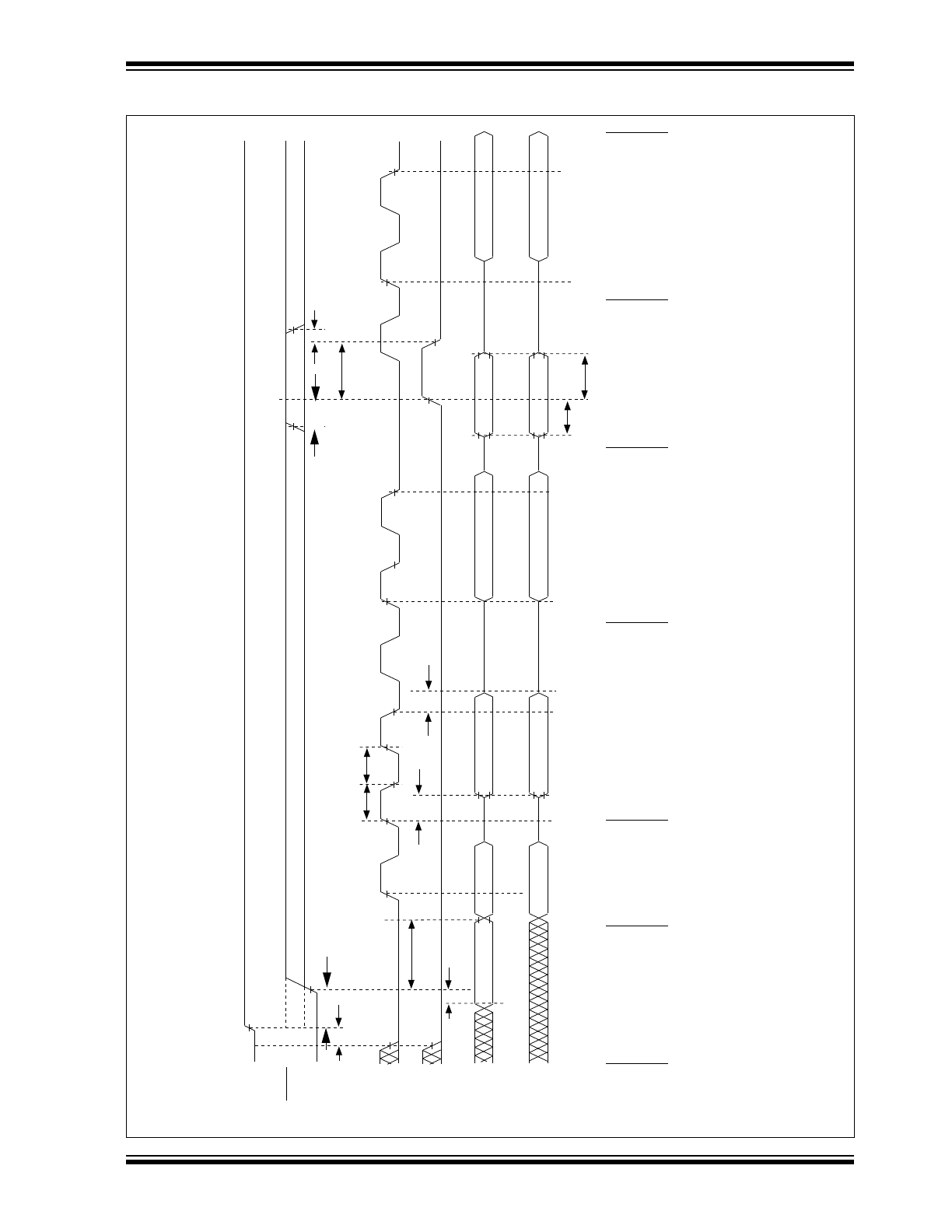
PROGRAMMING AND VERIFY TIMINGS I
Test
13V
V
PP
/MCLR
5V
tirV2tsH
ttsH2mcH
RA1
RA0
E1H
RB<7:0>
Jump Address
Input
ADDR_HI
DATA_HI OUT
DATA_HI OUT
RC<7:0>
ADDR_LO
DATA_LO OUT
DATA_LO OUT
DATA_LO_IN
DATA_LO OUT
tmcH2rbL
tirH2lrL
tirL2lrH
tra1H2bcV
tra1L2bcZ
DATA_HI OUT
INC
ADDR
DATA_HI_IN
Programming
Mode entry
Load address X
Verify location X
Increment address to X + 1
by pulsing RA1
Verify location X + 1
Program location X + 1
Do not increment PC
by raising RA1 before
RA0
↓
Verify location X + 1
tbcV2irH
tirH2bc
I
tvpps
tvppH
tprog
trbV2mcH
Note:
RA2 = 0
RA3 = 0
RA4 = 1
P15
P14
P9
P1
1
P10
P8
P7
P3
P4
P17
P18
P5
P6
PIC17CXX
DS30139I-page 12
1996 Microchip Technology Inc.
FIGURE 5-2:
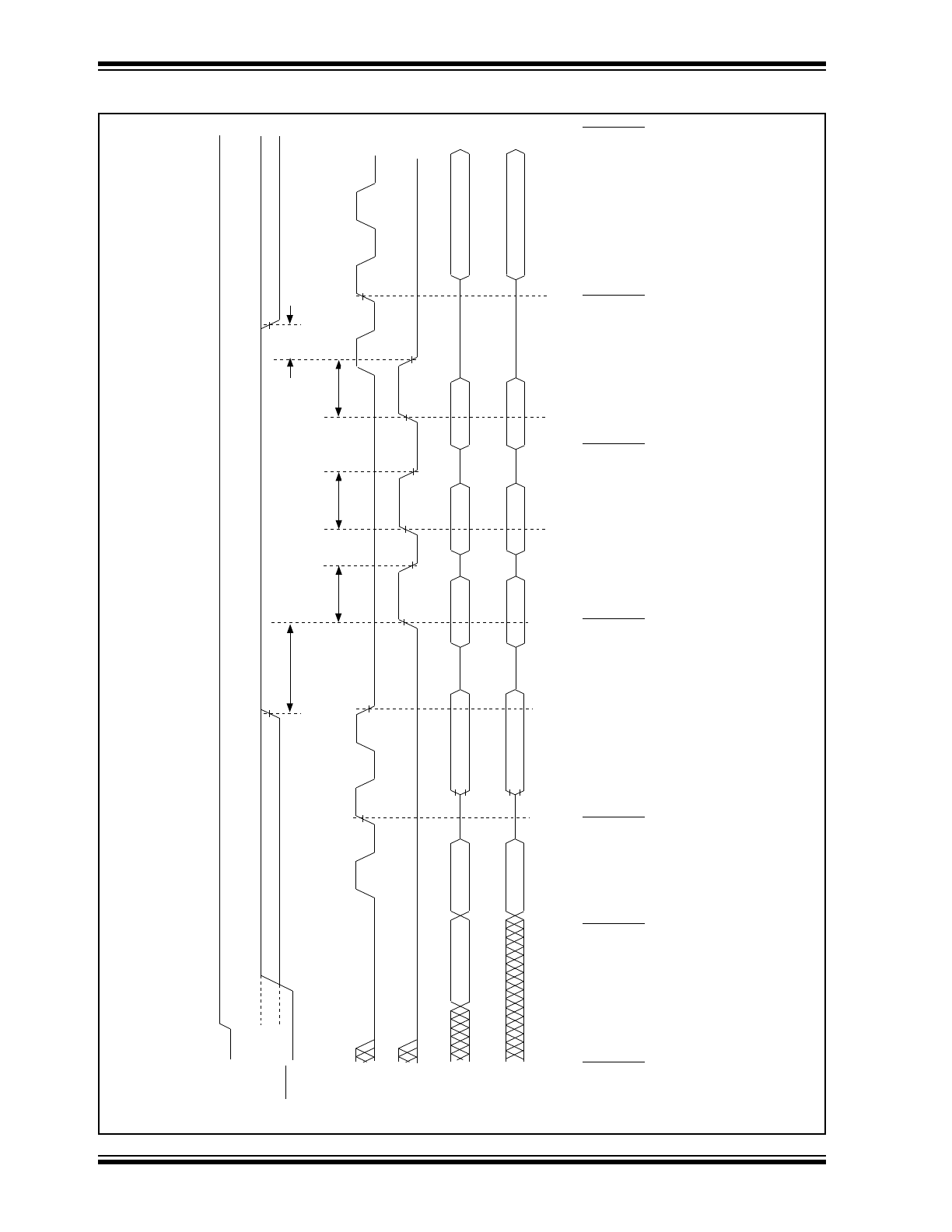
PROGRAMMING AND VERIFY TIMINGS II
Test
13V
V
PP
/MCLR
5V
RA1
RA0
E1H
RB<7:0>
Jump Address
Input
ADDR_HI
DATA_HI OUT
RC<7:0>
ADDR_LO
DATA_LO OUT
DATA_LO_IN
DATA_LO_IN
Programming
mode entry
Load address X
Verify location X
Program location X
Program location X
Move to verify cycle
Prevent increment of
PC by raising RA1
before RA0
↓
Verify location X
tvpps
tvppH
tprog
tprog
DATA_HI_IN
tprog
DATA_HI_IN
DATA_HI_IN
DATA_HI OUT
DATA_LO OUT
DATA_LO_IN
Note:
RA2 = 0
RA3 = 0
RA4 = 1
P15
P9
P9
P9
P14
1996 Microchip Technology Inc.
DS30139I-page 13
EPROM Memory Programming Specification
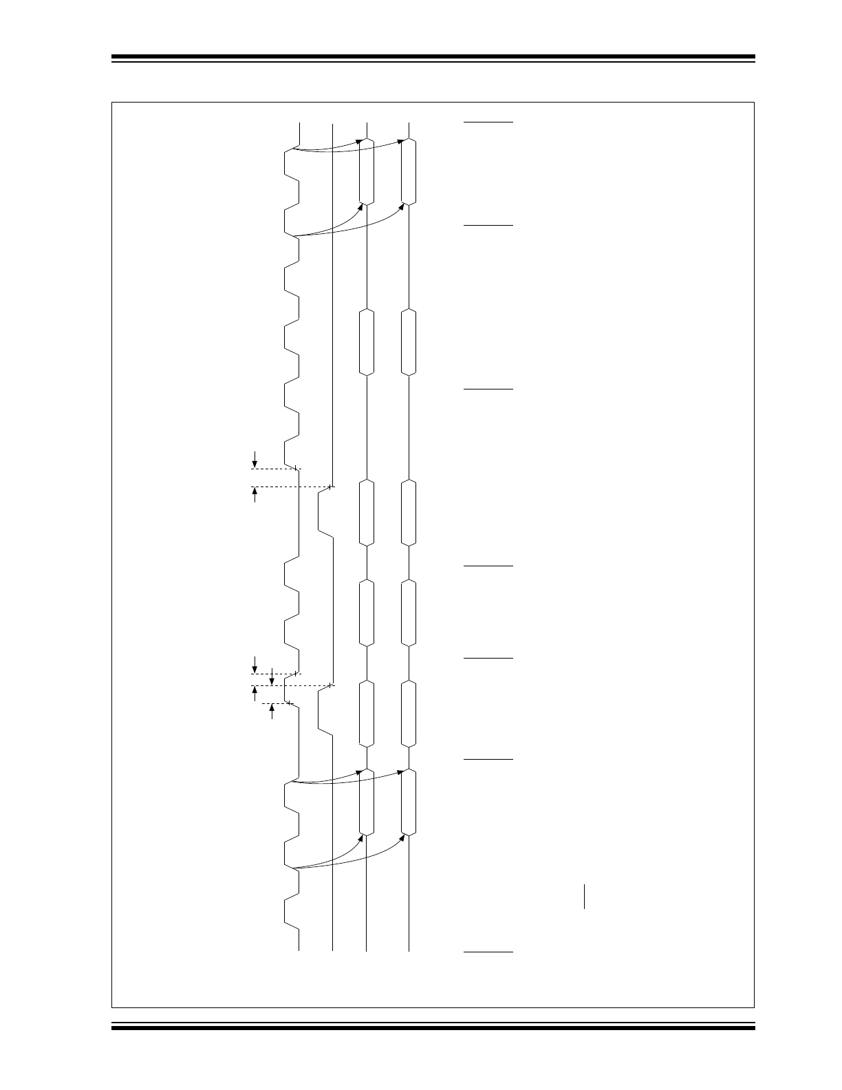
FIGURE 5-3:
PROGRAMMING AND VERIFY TIMINGS III
RA1
RA0
RB<7:0>
RC<7:0>
Verify location X
Verify location X
Verify location X +1
Pulse RA1 to increment
address to X +2
INC PC
tinL2ra1l
tra1V2inL
tinL2ra1l
INC PC
INC PC
DATA_HI OUT
DATA_HI IN
DATA_HI OUT
DATA_HI IN
DATA_HI OUT
DATA_HI OUT
DATA_LO OUT
DATA_LO IN
DATA_LO OUT
DATA_LO IN
DATA_LO OUT
DATA_LO OUT
Verify location X +2
Program location X
Do not increment PC
Raise RA1 before
RA0
↓
to do this
Program location X
Raise RA1 after RA0
↓
to increment to location X +1
Note:
Device in PGM mode
Test = +5
V
PP
/MCLR = V
PP
RA2 = 0
RA3 = 0
RA4 = 1
P13
P13
P12
PIC17CXX
DS30139I-page 14
1996 Microchip Technology Inc.
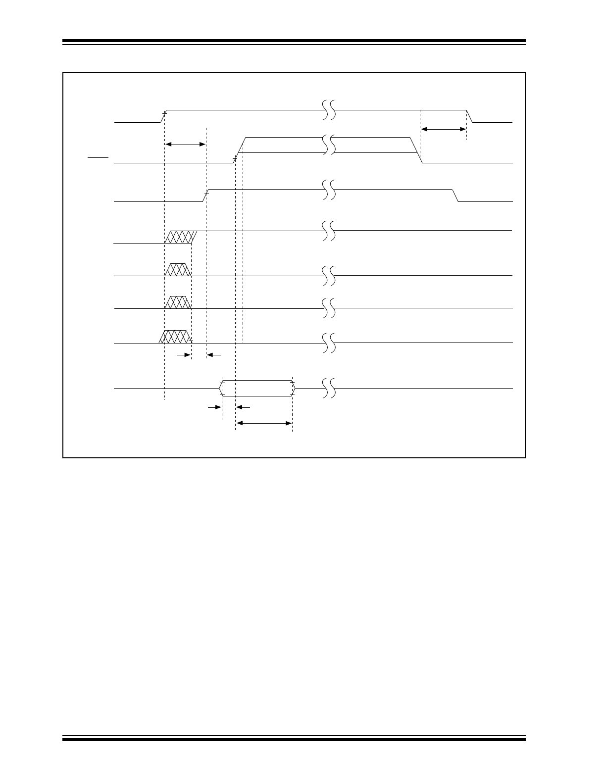
FIGURE 5-4:
POWER-UP/DOWN SEQUENCE FOR PROGRAMMING
V
DD
V
PP
/MCLR
TEST
tvpL2vcL
tvcV2tsH
RA0
tirV2tsH
E1H
RB<7:0>
trbV2mcH
tmcH2rbI
RA2
RA3
RA4
P16
P19
P3
P17
P18

1996 Microchip Technology Inc.
DS30139I-page 15
EPROM Memory Programming Specification
NOTES:
Information contained in this publication regarding device applications and the like is intended for suggestion only and may be superseded by updates. No representation or warranty is given and no liability is assumed
by Microchip Technology Incorporated with respect to the accuracy or use of such information, or infringement of patents or other intellectual property rights arising from such use or otherwise. Use of Microchip’s products
as critical components in life support systems is not authorized except with express written approval by Microchip. No licenses are conveyed, implicitly or otherwise, under any intellectual property rights. The Microchip
logo and name are registered trademarks of Microchip Technology Inc. in the U.S.A. and other countries. All rights reserved. All other trademarks mentioned herein are the property of their respective companies.
1999 Microchip Technology Inc.
All rights reserved. © 1999 Microchip Technology Incorporated. Printed in the USA. 11/99
Printed on recycled paper.
AMERICAS
Corporate Office
Microchip Technology Inc.
2355 West Chandler Blvd.
Chandler, AZ 85224-6199
Tel: 480-786-7200 Fax: 480-786-7277
Technical Support: 480-786-7627
Web Address: http://www.microchip.com
Atlanta
Microchip Technology Inc.
500 Sugar Mill Road, Suite 200B
Atlanta, GA 30350
Tel: 770-640-0034 Fax: 770-640-0307
Boston
Microchip Technology Inc.
5 Mount Royal Avenue
Marlborough, MA 01752
Tel: 508-480-9990 Fax: 508-480-8575
Chicago
Microchip Technology Inc.
333 Pierce Road, Suite 180
Itasca, IL 60143
Tel: 630-285-0071 Fax: 630-285-0075
Dallas
Microchip Technology Inc.
4570 Westgrove Drive, Suite 160
Addison, TX 75248
Tel: 972-818-7423 Fax: 972-818-2924
Dayton
Microchip Technology Inc.
Two Prestige Place, Suite 150
Miamisburg, OH 45342
Tel: 937-291-1654 Fax: 937-291-9175
Detroit
Microchip Technology Inc.
Tri-Atria Office Building
32255 Northwestern Highway, Suite 190
Farmington Hills, MI 48334
Tel: 248-538-2250 Fax: 248-538-2260
Los Angeles
Microchip Technology Inc.
18201 Von Karman, Suite 1090
Irvine, CA 92612
Tel: 949-263-1888 Fax: 949-263-1338
New York
Microchip Technology Inc.
150 Motor Parkway, Suite 202
Hauppauge, NY 11788
Tel: 631-273-5305 Fax: 631-273-5335
San Jose
Microchip Technology Inc.
2107 North First Street, Suite 590
San Jose, CA 95131
Tel: 408-436-7950 Fax: 408-436-7955
AMERICAS
(continued)
Toronto
Microchip Technology Inc.
5925 Airport Road, Suite 200
Mississauga, Ontario L4V 1W1, Canada
Tel: 905-405-6279 Fax: 905-405-6253
ASIA/PACIFIC
Hong Kong
Microchip Asia Pacific
Unit 2101, Tower 2
Metroplaza
223 Hing Fong Road
Kwai Fong, N.T., Hong Kong
Tel: 852-2-401-1200 Fax: 852-2-401-3431
Beijing
Microchip Technology, Beijing
Unit 915, 6 Chaoyangmen Bei Dajie
Dong Erhuan Road, Dongcheng District
New China Hong Kong Manhattan Building
Beijing 100027 PRC
Tel: 86-10-85282100 Fax: 86-10-85282104
India
Microchip Technology Inc.
India Liaison Office
No. 6, Legacy, Convent Road
Bangalore 560 025, India
Tel: 91-80-229-0061 Fax: 91-80-229-0062
Japan
Microchip Technology Intl. Inc.
Benex S-1 6F
3-18-20, Shinyokohama
Kohoku-Ku, Yokohama-shi
Kanagawa 222-0033 Japan
Tel: 81-45-471- 6166 Fax: 81-45-471-6122
Korea
Microchip Technology Korea
168-1, Youngbo Bldg. 3 Floor
Samsung-Dong, Kangnam-Ku
Seoul, Korea
Tel: 82-2-554-7200 Fax: 82-2-558-5934
Shanghai
Microchip Technology
RM 406 Shanghai Golden Bridge Bldg.
2077 Yan’an Road West, Hong Qiao District
Shanghai, PRC 200335
Tel: 86-21-6275-5700 Fax: 86 21-6275-5060
ASIA/PACIFIC
(continued)
Singapore
Microchip Technology Singapore Pte Ltd.
200 Middle Road
#07-02 Prime Centre
Singapore 188980
Tel: 65-334-8870 Fax: 65-334-8850
Taiwan, R.O.C
Microchip Technology Taiwan
10F-1C 207
Tung Hua North Road
Taipei, Taiwan, ROC
Tel: 886-2-2717-7175 Fax: 886-2-2545-0139
EUROPE
United Kingdom
Arizona Microchip Technology Ltd.
505 Eskdale Road
Winnersh Triangle
Wokingham
Berkshire, England RG41 5TU
Tel: 44 118 921 5858 Fax: 44-118 921-5835
Denmark
Microchip Technology Denmark ApS
Regus Business Centre
Lautrup hoj 1-3
Ballerup DK-2750 Denmark
Tel: 45 4420 9895 Fax: 45 4420 9910
France
Arizona Microchip Technology SARL
Parc d’Activite du Moulin de Massy
43 Rue du Saule Trapu
Batiment A - ler Etage
91300 Massy, France
Tel: 33-1-69-53-63-20 Fax: 33-1-69-30-90-79
Germany
Arizona Microchip Technology GmbH
Gustav-Heinemann-Ring 125
D-81739 München, Germany
Tel: 49-89-627-144 0 Fax: 49-89-627-144-44
Italy
Arizona Microchip Technology SRL
Centro Direzionale Colleoni
Palazzo Taurus 1 V. Le Colleoni 1
20041 Agrate Brianza
Milan, Italy
Tel: 39-039-65791-1 Fax: 39-039-6899883
11/15/99
W
ORLDWIDE
S
ALES
AND
S
ERVICE
Microchip received QS-9000 quality system
certification for its worldwide headquarters,
design and wafer fabrication facilities in
Chandler and Tempe, Arizona in July 1999. The
Company’s quality system processes and
procedures are QS-9000 compliant for its
PICmicro
®
8-bit MCUs, K
EE
L
OQ
®
code hopping
devices, Serial EEPROMs and microperipheral
products. In addition, Microchip’s quality
system for the design and manufacture of
development systems is ISO 9001 certified.