
© 2006-2011 Microchip Technology Inc.
DS22011B-page 1
MCP3905A/05L/06A
Features
• Supplies active
(real) power measurement for
single-phase, residential energy metering
• Supports IEC 62053 International Energy
Metering Specification and legacy IEC
1036/61036/687 Specifications
• Two multi-bit, DAC, second-order, 16-bit, Delta-
Sigma Analog-to-Digital Converters (ADCs)
• Reduced pulse-width of calibration output
frequency and mechanical counter drive for low
power meter designs (MCP3905L)
• Increased output frequency constant options for
meter design (MCP3905L)
• 0.1% typical measurement error over 500:1
dynamic range (MCP3905A / MCP3905L)
• 0.1% typical measurement error over 1000:1
dynamic range (MCP3906A)
• Programmable Gain Amplifier (PGA) for small
signal inputs supports low value shunt current
sensor:
- 16:1 PGA - MCP3905A / MCP3905L
- 32:1 PGA - MCP3906A
• Ultra-low drift on-chip reference:
15 ppm/°C (typical)
• Direct drive for electromagnetic mechanical
counter and two-phase stepper motors
• Low I
DD
of 4 mA (typical)
• Tamper output pin for negative power indication
• Industrial Temperature Range: -40°C to +85°C
• Extended Temperature Range: -40°C to +125°C
• Supplies instantaneous real power on HF
OUT
for
meter calibration
Description
The MCP3905A/05L/06A devices are energy-metering
ICs designed to support the IEC 62053 international
metering standard specification. They supply a
frequency output proportional to the average active real
power, as well as a higher-frequency output
proportional to the instantaneous power for meter
calibration. The MCP3905L offers reduced pulse width
of calibration output frequency and mechanical counter
drive for lower power meter designs. They include two
16-bit, Delta-Sigma ADCs for a wide range of I
B
and
I
MAX
currents and/or small shunt (<200 µOhms) meter
designs. It includes an ultra-low drift voltage reference
with < 15 ppm/°C through a specially designed band
gap temperature curve for the minimum gradient
across the industrial temperature range. A fixed-
function DSP block is on-chip for active real-power
calculation. A no-load threshold block prevents any
current creep measurements. A Power-On Reset
(POR) block restricts meter performance during low-
voltage situations. These accurate energy metering ICs
with high field reliability are available in the industry
standard pinout.
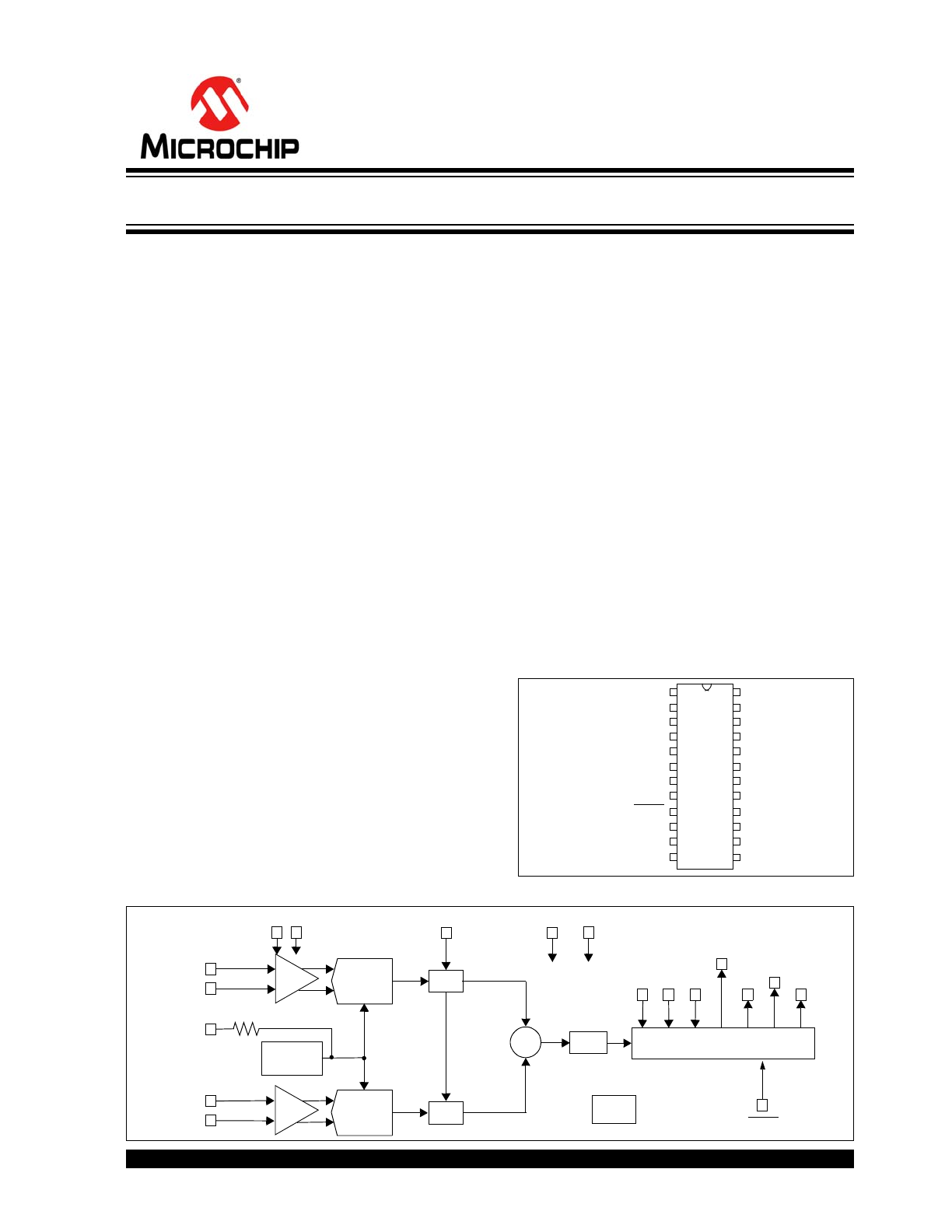
Package Type
Functional Block Diagram
F
OUT0
D
GND
NEG
1
2
3
4
24
23
22
21
20
19
18
17
5
6
7
8
F
OUT1
NC
OSC2
OSC1
DV
DD
HPF
AV
DD
NC
CH0+
CH0-
CH1-
CH1+
HF
OUT
16
9
G0
MCLR
15
14
10
11
G1
F0
REFIN/OUT
A
GND
13
12
F1
F2
24-Pin SSOP
16-bit
ΔΣ ADC
MCLR
+
–
CH0+
CH0-
Reference
2.4V
+
–
CH1+
CH1-
HPF1
LPF1
E-to-F
conversion
REFIN/
F
OUT1
HF
OUT
G0 G1
F2
F1
F
OUT0
OSC1 OSC2
OUT
NEG
HPF
F0
Multi-level
16-bit
ΔΣ ADC
Multi-level
X
HPF1
PGA
POR
Energy Metering ICs with Active Real Power Pulse Output

MCP3905A/05L/06A
DS22011B-page 2
© 2006-2011 Microchip Technology Inc.
NOTES:
© 2006-2011 Microchip Technology Inc.
DS22011B-page 3
MCP3905A/05L/06A
1.0
ELECTRICAL
CHARACTERISTICS
Absolute Maximum Ratings †
V
DD
...................................................................................7.0V
Digital inputs and outputs w.r.t. A
GND
........ -0.6V to V
DD
+0.6V
Analog input w.r.t. A
GND
..................................... ....-6V to +6V
V
REF
input w.r.t. A
GND
............................... -0.6V to V
DD
+0.6V
Storage temperature .....................................-65°C to +150°C
Ambient temp. with power applied ................-65°C to +125°C
Soldering temperature of leads (10 seconds) ............. +300°C
ESD on the analog inputs (HBM,MM) ................. 5.0 kV, 500V
ESD on all other pins (HBM,MM) ........................ 5.0 kV, 500V
† Notice: Stresses above those listed under “Maximum
Ratings” may cause permanent damage to the device.
This is a stress rating only and functional operation of
the device at those or any other conditions above those
indicated in the operation listings of this specification is
not implied. Exposure to maximum rating conditions for
extended periods may affect device reliability.
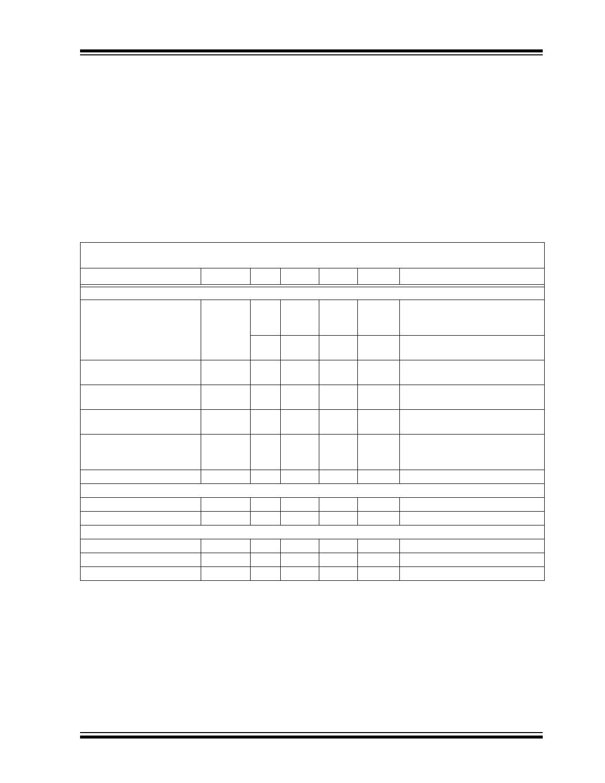
ELECTRICAL CHARACTERISTICS
Electrical Specifications: Unless otherwise indicated, all parameters apply at AV
DD
= DV
DD
= 4.5V – 5.5V,
Internal V
REF
, HPF turned on (AC mode), A
GND
, D
GND
= 0V, MCLK = 3.58 MHz; T
A
= -40°C to +85°C.
Parameter
Sym
Min
Typ
Max
Units
Comment
Overall Measurement Accuracy
Energy Measurement Error
E
—
0.1
—
% F
OUT
Channel 0 swings 1:500 range,
MCP3905A, MCP3905L only
(
Note 1
,
Note 4
)
—
0.1
—
% F
OUT
Channel 0 swings 1:1000 range,
MCP3906A only (
Note 1
,
Note 4
)
No-Load Threshold/
Minimum Load
NLT
—
0.0015
—
% F
OUT
Max
Disabled when F2, F1, F0 = 0, 1, 1
(
Note 5
,
Note 6
)
Phase Delay Between
Channels
—
—
1/MCLK
s
HPF = 0 and 1, < 1 MCLK
(
Note 4
,
Note 6
,
Note 7
)
AC Power Supply Rejection
(output frequency variation)
AC PSRR
—
0.01
—
% F
OUT
F2, F1, F0 = 0, 1, 1 (
Note 3
)
DC Power Supply Rejection
(output frequency
variation)
DC PSRR
—
0.01
—
% F
OUT
HPF = 1, Gain = 1 (
Note 3
)
System Gain Error
—
3
10
% F
OUT
(
Note 2
,
Note 5
)
ADC/PGA Specifications
Offset Error
V
OS
—
2
5
mV
Referred to Input
Gain Error Match
—
0.5
—
% F
OUT
(
Note 5
)
Internal Voltage Reference
Voltage
—
2.4
—
V
Tolerance
—
±2
—
%
Tempco
—
15
—
ppm/°C
Note 1:
Measurement error = (Energy Measured By Device - True Energy)/True Energy * 100%. Accuracy is
measured with signal (±660 mV) on Channel 1. F
OUT0
, F
OUT1
pulse outputs. Valid from 45 Hz to 65 Hz.
See typical performance curves for higher frequencies and increased dynamic range.
2:
Does not include internal V
REF
. Gain = 1, CH0 = 470 mVDC, CH1 = 660 mVDC, difference between
measured output frequency and expected transfer function.
3:
Percent of HF
OUT
output frequency variation; Includes external V
REF
= 2.5V, CH1 = 100 mVRMS @
50 Hz, CH2 = 100 mVRMS @ 50 Hz, AV
DD
= 5V + 1V
pp
@ 100 Hz. DC PSRR: 5V ±500 mV
4:
Error applies down to 60 degree lead (PF = 0.5 capacitive) and 60 degree lag (PF = 0.5 inductive).
5:
Refer to
Section 4.0 “Device Overview”
for complete description.
6:
Specified by characterization, not production tested.
7:
1 MCLK period at 3.58 MHz is equivalent to less than <0.005 degrees at 50 or 60 Hz.
MCP3905A/05L/06A
DS22011B-page 4
© 2006-2011 Microchip Technology Inc.
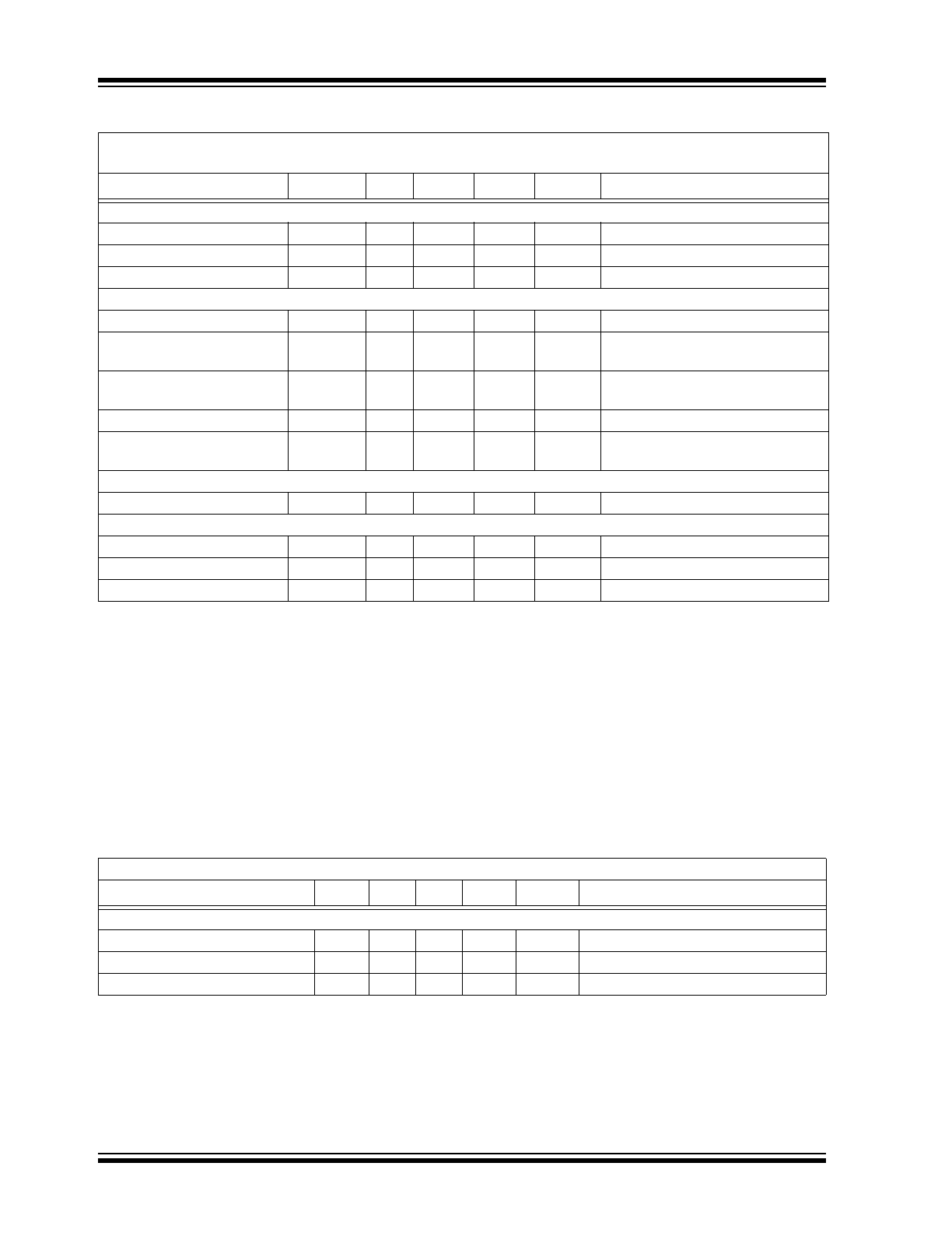
Reference Input
Input Range
2.2
—
2.6
V
Input Impedance
3.2
—
—
k
Ω
Input Capacitance
—
—
10
pF
Analog Inputs
Maximum Signal Level
—
—
±1
V
CH0+,CH0-,CH1+,CH1- to A
GND
Differential Input Voltage
Range Channel 0
—
—
±470/G
mV
G = PGA Gain on Channel 0
Differential Input Voltage
Range Channel 1
—
—
±660
mV
Input Impedance
390
—
—
k
Ω
Proportional to 1/MCLK frequency
Bandwidth
(Notch Frequency)
—
14
—
kHz
Proportional to MCLK frequency,
MCLK/256
Oscillator Input
Frequency Range
MCLK
1
—
4
MHz
Power Specifications
Operating Voltage
4.5
—
5.5
V
AV
DD,
DV
DD
I
DD,A
I
DD,A
—
2.7
3.0
mA
AV
DD
pin only
I
DD,D
I
DD,D
—
1.2
2.0
mA
DV
DD
pin only
TEMPERATURE CHARACTERISTICS
Electrical Specifications: Unless otherwise indicated, V
DD
= 4.5V – 5.5V, A
GND
, D
GND
= 0V.
Parameters
Sym
Min
Typ
Max
Units
Conditions
Temperature Ranges
Specified Temperature Range
T
A
-40
—
+85
°C
Operating Temperature Range
T
A
-40
—
+125
°C
(
Note
)
Storage Temperature Range
T
A
-65
—
+150
°C
Note:
The MCP3905A/05L/06A operate over this extended temperature range, but with reduced performance. In
any case, the Junction Temperature (T
J
) must not exceed the Absolute Maximum specification of +150°C.
ELECTRICAL CHARACTERISTICS (CONTINUED)
Electrical Specifications: Unless otherwise indicated, all parameters apply at AV
DD
= DV
DD
= 4.5V – 5.5V,
Internal V
REF
, HPF turned on (AC mode), A
GND
, D
GND
= 0V, MCLK = 3.58 MHz; T
A
= -40°C to +85°C.
Parameter
Sym
Min
Typ
Max
Units
Comment
Note 1:
Measurement error = (Energy Measured By Device - True Energy)/True Energy * 100%. Accuracy is
measured with signal (±660 mV) on Channel 1. F
OUT0
, F
OUT1
pulse outputs. Valid from 45 Hz to 65 Hz.
See typical performance curves for higher frequencies and increased dynamic range.
2:
Does not include internal V
REF
. Gain = 1, CH0 = 470 mVDC, CH1 = 660 mVDC, difference between
measured output frequency and expected transfer function.
3:
Percent of HF
OUT
output frequency variation; Includes external V
REF
= 2.5V, CH1 = 100 mVRMS @
50 Hz, CH2 = 100 mVRMS @ 50 Hz, AV
DD
= 5V + 1V
pp
@ 100 Hz. DC PSRR: 5V ±500 mV
4:
Error applies down to 60 degree lead (PF = 0.5 capacitive) and 60 degree lag (PF = 0.5 inductive).
5:
Refer to
Section 4.0 “Device Overview”
for complete description.
6:
Specified by characterization, not production tested.
7:
1 MCLK period at 3.58 MHz is equivalent to less than <0.005 degrees at 50 or 60 Hz.
© 2006-2011 Microchip Technology Inc.
DS22011B-page 5
MCP3905A/05L/06A
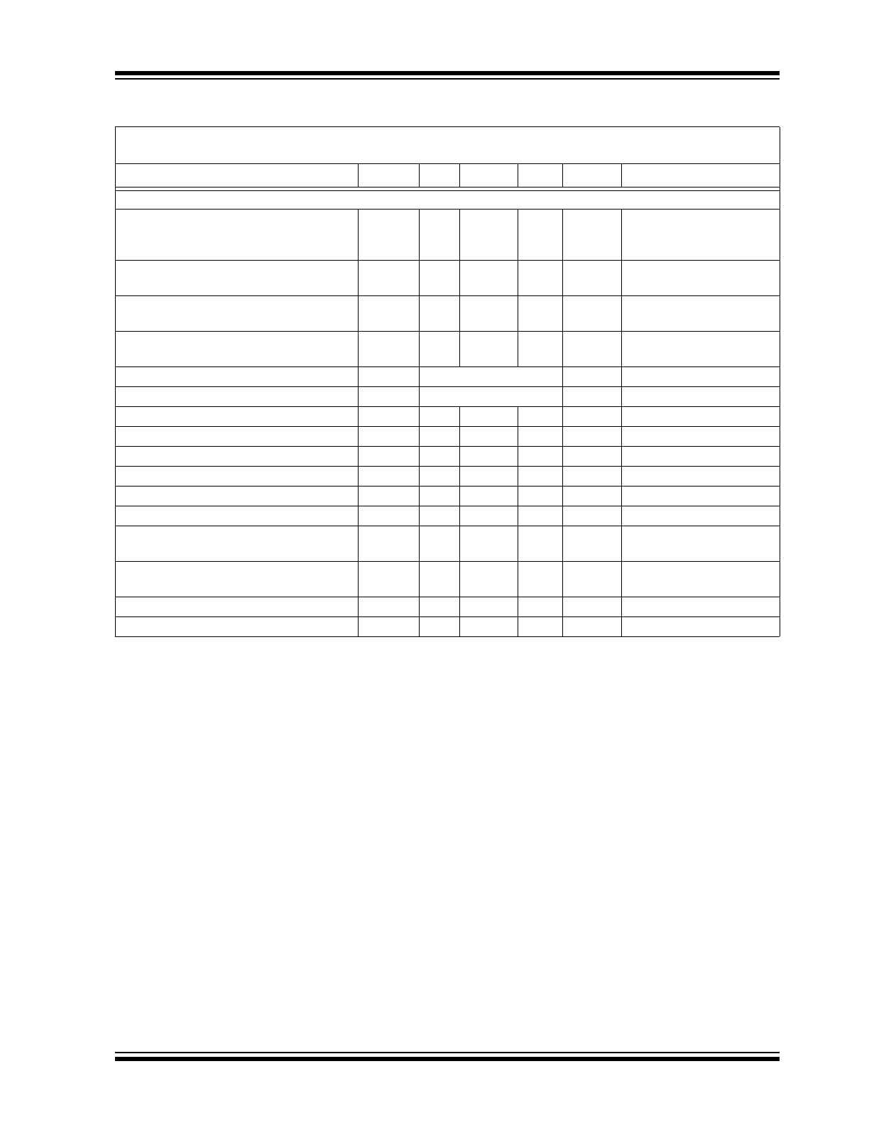
TIMING CHARACTERISTICS
Electrical Specifications: Unless otherwise indicated, all parameters apply at AV
DD
= DV
DD
= 4.5V – 5.5V,
A
GND
, D
GND
= 0V, MCLK = 3.58 MHz; T
A
= -40°C to +85°C.
Parameter
Sym
Min
Typ
Max
Units
Comment
Frequency Output
F
OUT0
and F
OUT1
Pulse Width
(Logic Low) for MCP3905A, MCP3906A
devices
t
FW
—
275
—
ms
984376 MCLK periods
(
Note 1
)
HF
OUT
Pulse Width for MCP3905A,
MCP3906A devices
t
HW
—
90
—
ms
322160 MCLK periods
(
Note 2
)
F
OUT0
and F
OUT1
Pulse Width
(Logic Low) for MCP3905L device
t
FW
—
130
—
ms
465344 MCLK periods
(
Note 1
)
HF
OUT
Pulse Width for MCP3905L
device
t
HW
—
65
—
ms
232672 MCLK periods
(
Note 2
)
F
OUT0
and F
OUT1
Pulse Period
t
FP
Refer to
Equation 4-1
s
HF
OUT
Pulse Period
t
HP
Refer to
Equation 4-2
s
F
OUT0
to F
OUT1
Falling-Edge Time
t
FS2
—
0.5 t
FP
—
F
OUT0
to F
OUT1
Min Separation
t
FS
—
4/MCLK
—
F
OUT0
and F
OUT1
Output High Voltage
V
OH
4.5
—
—
V
I
OH
= 10 mA, DV
DD
= 5.0V
F
OUT0
and F
OUT1
Output Low Voltage
V
OL
—
—
0.5
V
I
OL
= 10 mA, DV
DD
= 5.0V
HF
OUT
Output High Voltage
V
OH
4.0
—
—
V
I
OH
= 5 mA, DV
DD
= 5.0V
HF
OUT
Output Low Voltage
V
OL
—
—
0.5
V
I
OL
= 5 mA, DV
DD
= 5.0V
High-Level Input Voltage
(All Digital Input Pins)
V
IH
2.4
—
—
V
DV
DD
= 5.0V
Low Level Input Voltage
(All Digital Input Pins)
V
IL
—
—
0.85
V
DV
DD
= 5.0V
Input Leakage Current
—
—
±3
µA
V
IN
= 0, V
IN
= DV
DD
Pin Capacitance
—
—
10
pF
Note 3
Note 1:
If output pulse period (t
FP
) falls below 984376*2 MCLK periods for MCP3905A/6A and 465344*2 MCLK
periods for MCP3905L, then t
FW
= 1/2 t
FP
.
2:
If output pulse period (t
HP
) falls below 322160*2 MCLK periods for MCP3905A/6A and 232672*2 MCLK
periods for MCP3905L, then t
HW
= 1/2 t
HP
. When F2, F1,F0 = 011, t
HW
is fixed to 18 µs (64 MCLK
periods).
3:
Specified by characterization, not production tested.
MCP3905A/05L/06A
DS22011B-page 6
© 2006-2011 Microchip Technology Inc.
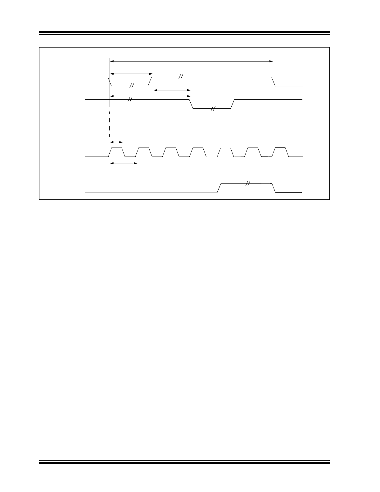
FIGURE 1-1:
Output Timings for Pulse Outputs and Negative Power Pin.
F
OUT0
t
FP
F
OUT1
HF
OUT
t
FW
t
HP
t
HW
t
FS
t
FS2
NEG
© 2006-2011 Microchip Technology Inc.
DS22011B-page 7
MCP3905A/05L/06A
2.0
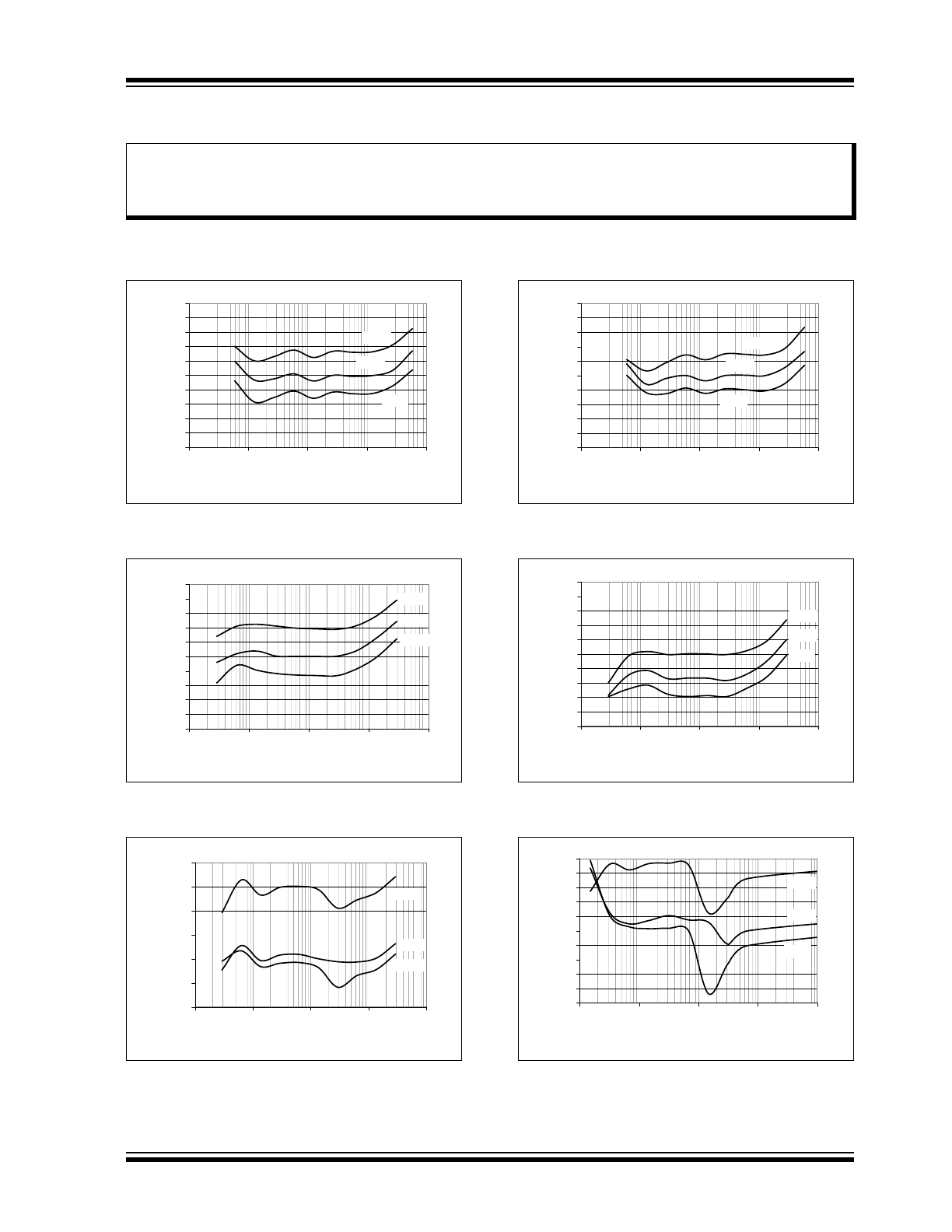
TYPICAL PERFORMANCE CURVES
Note: Unless otherwise specified, DV
DD
, AV
DD
= 5V; A
GND
, D
GND
= 0V; V
REF
= Internal, HPF = 1 (AC mode),
MCLK = 3.58 MHz.
FIGURE 2-1:
Measurement Error,
Gain = 8 PF = 1.
FIGURE 2-2:
Measurement Error,
Gain = 16, PF = 1.
FIGURE 2-3:
Measurement Error,
Gain = 32, PF = 1.
FIGURE 2-4:
Measurement Error,
Gain = 8, PF = 0.5.
FIGURE 2-5:
Measurement Error,
Gain = 16, PF = 0.5.
FIGURE 2-6:
Measurement Error,
Gain =32, PF = 0.5.
Note:
The graphs and tables provided following this note are a statistical summary based on a limited number of
samples and are provided for informational purposes only. The performance characteristics listed herein
are not tested or guaranteed. In some graphs or tables, the data presented may be outside the specified
operating range (e.g., outside specified power supply range) and therefore outside the warranted range.
-0.5
-0.4
-0.3
-0.2
-0.1
0
0.1
0.2
0.3
0.4
0.5
0.0000
0.0001
0.0010
0.0100
0.1000
CH1 Vp-p Amplitude (V)
M
eas
ur
e
m
en
t Er
ro
r
+85°C
+25°C
-40°C
`
-0.5
-0.4
-0.3
-0.2
-0.1
0
0.1
0.2
0.3
0.4
0.5
0.0000
0.0001
0.0010
0.0100
0.1000
CH1 Vp-p Amplitude (V)
M
e
a
s
u
remen
t E
rr
o
r
+85°C
+25°C
- 40°C
-0.5
-0.25
0
0.25
0.5
0.75
1
0.0000
0.0001
0.0010
0.0100
0.1000
CH1 Vp-p Amplitude (V)
Me
a
s
u
re
me
n
t E
rro
r
+85°C
+25°C
- 40°C
-0.5
-0.4
-0.3
-0.2
-0.1
0
0.1
0.2
0.3
0.4
0.5
0.0000
0.0001
0.0010
0.0100
0.1000
CH1 Vp-p Amplitude (V)
M
e
a
s
u
remen
t E
rr
o
r
+85°C
+25°C
-40°C
-0.5
-0.4
-0.3
-0.2
-0.1
0
0.1
0.2
0.3
0.4
0.5
0.0000
0.0001
0.0010
0.0100
0.1000
CH1 Vp-p Amplitude (V)
Me
a
s
u
re
me
n
t E
rro
r
+85°C
+25°C
-40°C
-1
-0.8
-0.6
-0.4
-0.2
0
0.2
0.4
0.6
0.8
1
0.0000
0.0001
0.0010
0.0100
0.1000
CH1 Vp-p Amplitude (V)
M
e
as
u
rem
e
n
t Er
ro
r
+85°C
+25°C
-40°C
MCP3905A/05L/06A
DS22011B-page 8
© 2006-2011 Microchip Technology Inc.
Note: Unless otherwise specified, DV
DD
, AV
DD
= 5V; A
GND
, D
GND
= 0V; V
REF
= Internal, HPF = 1 (AC mode),
MCLK = 3.58 MHz.
FIGURE 2-7:
Measurement Error,
Gain = 1, PF = 1.
FIGURE 2-8:
Measurement Error,
Gain = 2, PF = 1.
FIGURE 2-9:
Measurement Error,
Gain = 1, PF = + 0.5.
FIGURE 2-10:
Measurement Error,
Gain = 2, PF = + 0.5.
-0.5
-0.4
-0.3
-0.2
-0.1
0
0.1
0.2
0.3
0.4
0.5
0.0001
0.0010
0.0100
0.1000
1.0000
CH0 Vp-p Amplitude (V)
Measur
e
ment E
rr
o
r
+85°C
+25°C
- 40°C
-0.5
-0.4
-0.3
-0.2
-0.1
0
0.1
0.2
0.3
0.4
0.5
0.0001
0.0010
0.0100
0.1000
1.0000
CH0 Vp-p Amplitude (V)
Me
a
s
u
re
me
n
t E
rro
r
+85°C
+25°C
- 40°C
-0.5
-0.4
-0.3
-0.2
-0.1
0
0.1
0.2
0.3
0.4
0.5
0.0001
0.0010
0.0100
0.1000
1.0000
CH1 Vp-p Amplitude (V)
M
e
asu
re
me
nt
Er
ro
r
+85°C
+25°C
-40°C
-0.5
-0.4
-0.3
-0.2
-0.1
0
0.1
0.2
0.3
0.4
0.5
0.0001
0.0010
0.0100
0.1000
1.0000
CH1 Vp-p Amplitude (V)
M
e
a
s
u
remen
t E
rr
o
r
+85°C
+25°C
-40°C
© 2006-2011 Microchip Technology Inc.
DS22011B-page 9
MCP3905A/05L/06A
Note: Unless otherwise specified, DV
DD
, AV
DD
= 5V; A
GND
, D
GND
= 0V; V
REF
= Internal, HPF = 1 (AC mode),
MCLK = 3.58 MHz.
FIGURE 2-11:
Measurement Error,
Temperature = +125°C, Gain = 1.
FIGURE 2-12:
Measurement Error,
Temperature = +125°C, Gain = 2.
FIGURE 2-13:
Measurement Error,
Temperature = +125°C, Gain = 8.
FIGURE 2-14:
Measurement Error,
Temperature = +125°C, Gain = 16.
-1
-0.8
-0.6
-0.4
-0.2
0
0.2
0.4
0.6
0.8
1
0.0001
0.001
0.01
0.1
1
CH1 Vp-p Amplitude (V)
Measurement Error (%)
+25°C; PF = 1
+25°C; PF = 0.5
+125°C; PF = 0.5
+125°C; PF = 1
-1
-0.8
-0.6
-0.4
-0.2
0
0.2
0.4
0.6
0.8
1
0.0001
0.001
0.01
0.1
1
CH1 Vp-p Amplitude (V)
Measurement Error (%)
+25°C; PF = 1
+25°C; PF = 0.5
+125°C; PF = 1
+125°C; PF = 0.5
-1
-0.8
-0.6
-0.4
-0.2
0
0.2
0.4
0.6
0.8
1
0.0001
0.001
0.01
0.1
1
CH1 Vp-p Amplitude (V)
Measurement Error (%)
+125°C; PF = 1
+125°C; PF = 0.5
+25°C; PF = 1
+25°C; PF = 0.5
-1
-0.8
-0.6
-0.4
-0.2
0
0.2
0.4
0.6
0.8
1
0.0001
0.001
0.01
0.1
1
CH1 Vp-p Amplitude (V)
Measurement Error (%)
+25°C; PF = 1
+25°C; PF = 0.5
+125°C; PF = 1
+125°C; PF = 0.5
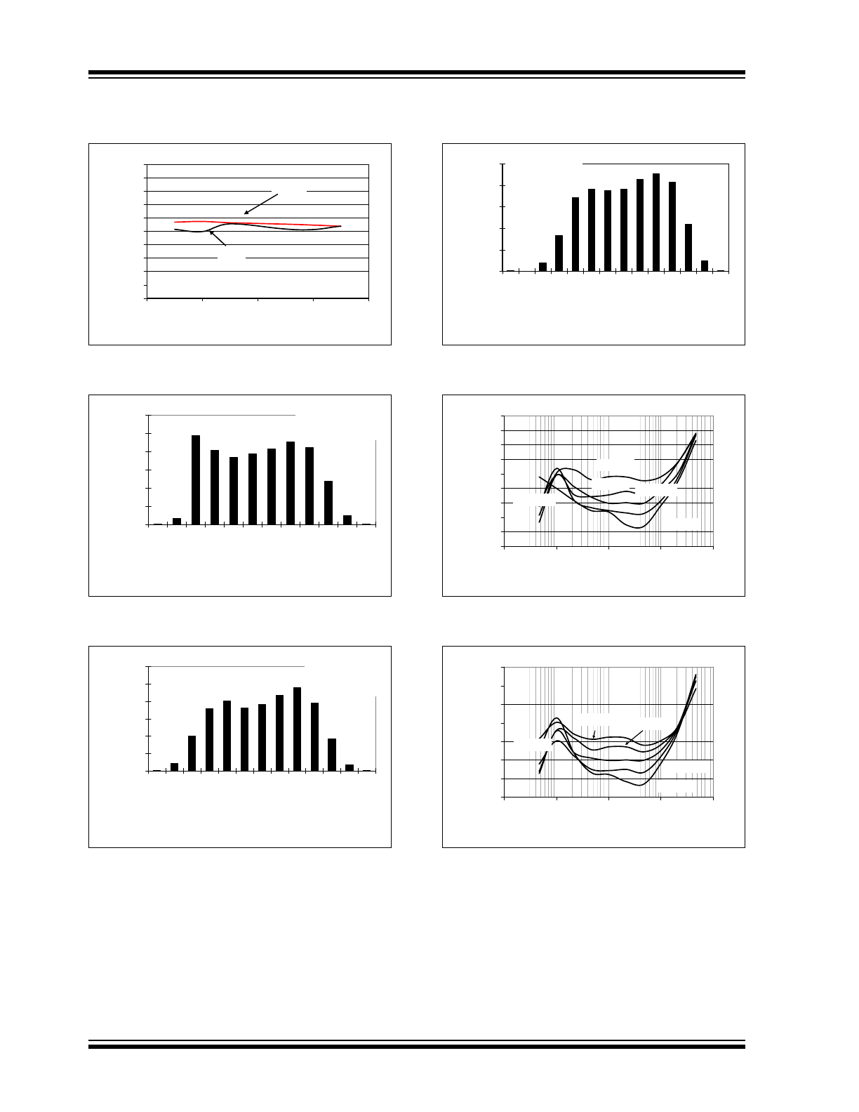
MCP3905A/05L/06A
DS22011B-page 10
© 2006-2011 Microchip Technology Inc.
Note: Unless otherwise specified, DV
DD
, AV
DD
= 5V; A
GND
, D
GND
= 0V; V
REF
= Internal, HPF = 1 (AC mode),
MCLK = 3.58 MHz.
FIGURE 2-15:
Measurement Error vs.
Input Frequency.
FIGURE 2-16:
Channel 0 Offset Error
(DC Mode, HPF off), G = 1.
FIGURE 2-17:
Channel 0 Offset Error
(DC Mode, HPF off), G = 8.
FIGURE 2-18:
Channel 0 Offset Error
(DC Mode, HPF Off), G = 16.
FIGURE 2-19:
Measurement Error vs. V
DD
(G = 16).
FIGURE 2-20:
Measurement Error vs. V
DD
,
G = 16, External V
REF
.
-0.5
-0.4
-0.3
-0.2
-0.1
0
0.1
0.2
0.3
0.4
0.5
40
50
60
70
80
Frequency (Hz)
M
easu
re
m
e
n
t E
rr
o
r (
%
)
PF = 0.5
PF = 1
0
500
1000
1500
2000
2500
3000
-4
.00
E
-3
-3
.95
E
-3
-3
.90
E
-3
-3
.85
E
-3
-3
.80
E
-3
-3
.75
E
-3
-3
.70
E
-3
-3
.65
E
-3
-3
.60
E
-3
-3
.55
E
-3
-3
.50
E
-3
-3
.45
E
-3
Channel 0 Offset (V)
Oc
c
u
ra
n
c
e
16384 Samples
Mean = -3.76 mV
Std. Dev = 110.4 µV
0
500
1000
1500
2000
2500
3000
-49
9
.6
E
-6
-49
4
.1
E
-6
-48
8
.6
E
-6
-48
3
.1
E
-6
-47
7
.6
E
-6
-47
2
.6
E
-6
-46
7
.1
E
-6
-46
1
.6
E
-6
-45
6
.1
E
-6
-45
0
.6
E
-6
-44
5
.6
E
-6
-44
0
.1
E
-6
-43
4
.6
E
-6
Channel 0 Offset (V)
Oc
c
u
ra
n
c
e
16384 Samples
Mean = -470.2 µV
Std. Dev = 13.8 µV
0
500
1000
1500
2000
2500
-25
1
.5
E
-6
-24
9
.5
E
-6
-24
8
.5
E
-6
-24
6
.5
E
-6
-24
3
.5
E
-6
-24
0
.5
E
-6
-23
7
.5
E
-6
-23
4
.5
E
-6
-23
1
.5
E
-6
-22
9
.5
E
-6
-22
6
.5
E
-6
-22
3
.5
E
-6
-22
0
.5
E
-6
-21
7
.5
E
-6
Channel 0 Offset (V)
O
ccu
ra
nc
e
16384 Samples
Mean = - 234.7 µV
Std. dev = - 6.91 µV
-0.15
-0.1
-0.05
0
0.05
0.1
0.15
0.2
0.25
0.3
0.0001
0.0010
0.0100
0.1000
1.0000
CH0 Vp-p Amplitude (V)
Mea
s
u
remen
t E
rr
o
r
V
DD
=4.75V
V
DD
=5.0V
V
DD
=4.5V
V
DD
=5.25V
V
DD
=5.5V
-0.1
-0.05
0
0.05
0.1
0.15
0.2
0.25
0.0001
0.0010
0.0100
0.1000
1.0000
CH0 Vp-p Amplitude (V)
M
e
as
u
rem
e
n
t E
rr
o
r
V
DD
=4.5V
V
DD
=4.75V
V
DD
=5.0V
V
DD
=5.25V
V
DD
=5.5V