

2010 Microchip Technology Inc.
DS39935C
ENC424J600/624J600
Data Sheet
Stand-Alone 10/100 Ethernet Controller
with SPI or Parallel Interface

DS39935C-page ii
2010 Microchip Technology Inc.
Information contained in this publication regarding device
applications and the like is provided only for your convenience
and may be superseded by updates. It is your responsibility to
ensure that your application meets with your specifications.
MICROCHIP MAKES NO REPRESENTATIONS OR
WARRANTIES OF ANY KIND WHETHER EXPRESS OR
IMPLIED, WRITTEN OR ORAL, STATUTORY OR
OTHERWISE, RELATED TO THE INFORMATION,
INCLUDING BUT NOT LIMITED TO ITS CONDITION,
QUALITY, PERFORMANCE, MERCHANTABILITY OR
FITNESS FOR PURPOSE. Microchip disclaims all liability
arising from this information and its use. Use of Microchip
devices in life support and/or safety applications is entirely at
the buyer’s risk, and the buyer agrees to defend, indemnify and
hold harmless Microchip from any and all damages, claims,
suits, or expenses resulting from such use. No licenses are
conveyed, implicitly or otherwise, under any Microchip
intellectual property rights.
Trademarks
The Microchip name and logo, the Microchip logo, dsPIC,
K
EE
L
OQ
, K
EE
L
OQ
logo, MPLAB, PIC, PICmicro, PICSTART,
rfPIC and UNI/O are registered trademarks of Microchip
Technology Incorporated in the U.S.A. and other countries.
FilterLab, Hampshire, HI-TECH C, Linear Active Thermistor,
MXDEV, MXLAB, SEEVAL and The Embedded Control
Solutions Company are registered trademarks of Microchip
Technology Incorporated in the U.S.A.
Analog-for-the-Digital Age, Application Maestro, CodeGuard,
dsPICDEM, dsPICDEM.net, dsPICworks, dsSPEAK, ECAN,
ECONOMONITOR, FanSense, HI-TIDE, In-Circuit Serial
Programming, ICSP, Mindi, MiWi, MPASM, MPLAB Certified
logo, MPLIB, MPLINK, mTouch, Octopus, Omniscient Code
Generation, PICC, PICC-18, PICDEM, PICDEM.net, PICkit,
PICtail, PIC
32
logo, REAL ICE, rfLAB, Select Mode, Total
Endurance, TSHARC, UniWinDriver, WiperLock and ZENA
are trademarks of Microchip Technology Incorporated in the
U.S.A. and other countries.
SQTP is a service mark of Microchip Technology Incorporated
in the U.S.A.
All other trademarks mentioned herein are property of their
respective companies.
© 2010, Microchip Technology Incorporated, Printed in the
U.S.A., All Rights Reserved.
Printed on recycled paper.
Note the following details of the code protection feature on Microchip devices:
•
Microchip products meet the specification contained in their particular Microchip Data Sheet.
•
Microchip believes that its family of products is one of the most secure families of its kind on the market today, when used in the
intended manner and under normal conditions.
•
There are dishonest and possibly illegal methods used to breach the code protection feature. All of these methods, to our
knowledge, require using the Microchip products in a manner outside the operating specifications contained in Microchip’s Data
Sheets. Most likely, the person doing so is engaged in theft of intellectual property.
•
Microchip is willing to work with the customer who is concerned about the integrity of their code.
•
Neither Microchip nor any other semiconductor manufacturer can guarantee the security of their code. Code protection does not
mean that we are guaranteeing the product as “unbreakable.”
Code protection is constantly evolving. We at Microchip are committed to continuously improving the code protection features of our
products. Attempts to break Microchip’s code protection feature may be a violation of the Digital Millennium Copyright Act. If such acts
allow unauthorized access to your software or other copyrighted work, you may have a right to sue for relief under that Act.
Microchip received ISO/TS-16949:2002 certification for its worldwide
headquarters, design and wafer fabrication facilities in Chandler and
Tempe, Arizona; Gresham, Oregon and design centers in California
and India. The Company’s quality system processes and procedures
are for its PIC
®
MCUs and dsPIC
®
DSCs, K
EE
L
OQ
®
code hopping
devices, Serial EEPROMs, microperipherals, nonvolatile memory and
analog products. In addition, Microchip’s quality system for the design
and manufacture of development systems is ISO 9001:2000 certified.
2010 Microchip Technology Inc.
DS39935C-page 1
ENC424J600/624J600
• IEEE 802.3™ Compliant Fast Ethernet Controller
• Integrated MAC and 10/100Base-T PHY
• Hardware Security Acceleration Engines
• 24-Kbyte Transmit/Receive Packet Buffer SRAM
• Supports one 10/100Base-T Port with Automatic
Polarity Detection and Correction
• Supports Auto-Negotiation
• Support for Pause Control Frames, including
Automatic Transmit and Receive Flow Control
• Supports Half and Full-Duplex Operation
• Programmable Automatic Retransmit on Collision
• Programmable Padding and CRC Generation
• Programmable Automatic Rejection of Erroneous
and Runt Packets
• Factory Preprogrammed Unique MAC Address
• MAC:
- Support for Unicast, Multicast and Broadcast
packets
- Supports promiscuous reception
- Programmable pattern matching
- Programmable filtering on multiple packet
formats, including Magic Packet™, Unicast,
Multicast, Broadcast, specific packet match,
destination address hash match or any packet
• PHY:
- Wave shaping output filter
- Internal Loopback mode
- Energy Detect Power-Down mode
• Available MCU Interfaces:
- 14 Mbit/s SPI interface with enhanced set of
opcodes (44-pin and 64-pin packages)
- 8-bit multiplexed parallel interface
(44-pin and 64-pin packages)
- 8-bit or 16-bit multiplexed or demultiplexed
parallel interface (64-pin package only)
• Security Engines:
- High-performance, modular exponentiation
engine with up to 1024-bit operands
- Supports RSA
®
and Diffie-Hellman key
exchange algorithms
- High-performance AES encrypt/decrypt
engine with 128-bit, 192-bit or 256-bit key
- Hardware AES ECB, CBC, CFB and OFB
mode capability
- Software AES CTR mode capability
- Fast MD5 hash computations
- Fast SHA-1 hash computations
• Buffer:
- Configurable transmit/receive buffer size
- Hardware-managed circular receive FIFO
- 8-bit or 16-bit random and sequential access
- High-performance internal DMA for fast
memory copying
- High-performance hardware IP checksum
calculations
- Accessible in low-power modes
- Space can be reserved for general purpose
application usage in addition to transmit and
receive packets
• Operational:
- Outputs for two LED indicators with support
for single and dual LED configurations
- Transmit and receive interrupts
- 25 MHz clock
- 5V tolerant inputs
- Clock out pin with programmable frequencies
from 50 kHz to 33.3 MHz
- Operating voltage range of 3.0V to 3.6V
- Temperature range: -40°C to +85°C industrial
• Available in 44-Pin (TQFP and QFN) and 64-Pin
TQFP Package
s
Device
SRAM
(bytes)
Pin
Count
Speed
(Mbps)
Security
SPI
PSP
ModEx
1024-Bit
MD5
SHA-1
AES
256-Bit
Multiplexed
Demultiplexed
8-
B
it
16
-B
it
8-
B
it
16
-B
it
ENC424J600
24K
44
10/100
Y
Y
Y
Y
Y
N
N
N
ENC624J600
24K
64
10/100
Y
Y
Y
Y
Y
Y
Y
Y
Stand-Alone 10/100 Ethernet Controller
with SPI or Parallel Interface
ENC424J600/624J600
DS39935C-page 2
2010 Microchip Technology Inc.
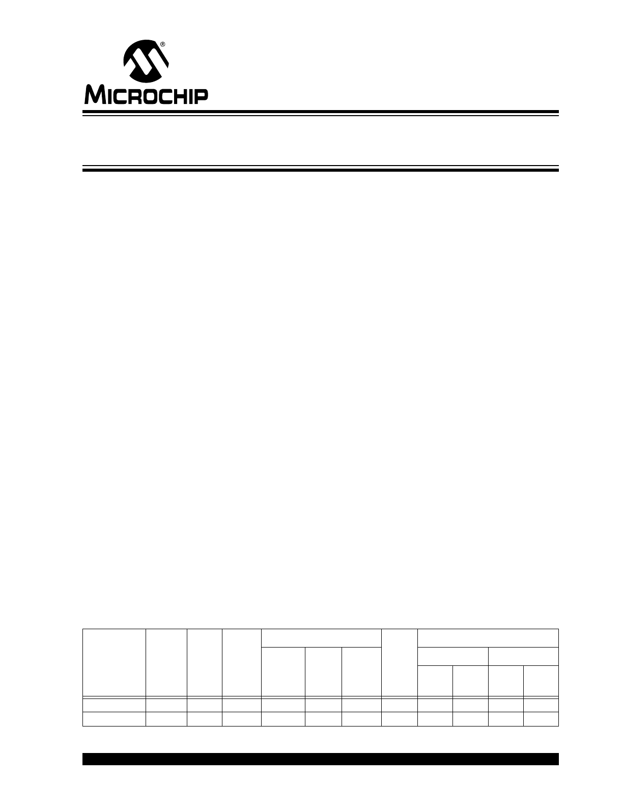
Pin Diagrams
44-Pin TQFP and QFN
10 11
2 3 4 5 6
1
18
19
20
21
22
12
13
14
15
38
8
7
44
43
42
41
40
39
16
17
29
30
31
32
33
23
24
25
26
27
28
36
34
35
9
37
ENC424J600
V
SSO
SC
AD4
OS
C2
OS
C1
V
DD
O
S
C
AD5
AD6
LE
D
B
LE
D
A
TPOUT+
TPOUT-
V
SSTX
AD9
AD1
0
AD1
1
AD1
2
SI/RD/RW
SCK/AL
V
SS
AD7
RB
IA
S
V
SSPLL
V
DDPLL
V
SSRX
V
DDTX
V
DDRX
TPIN-
TPIN+
INT
/S
PI
SE
L
CL
KOUT
AD8
PS
PCFG
0
AD1
4
V
SS
AD1
3
V
CAP
AD0
SO/WR/EN
CS/CS
AD1
AD2
V
DD
AD3
V
SSTX
2010 Microchip Technology Inc.
DS39935C-page 3
ENC424J600/624J600
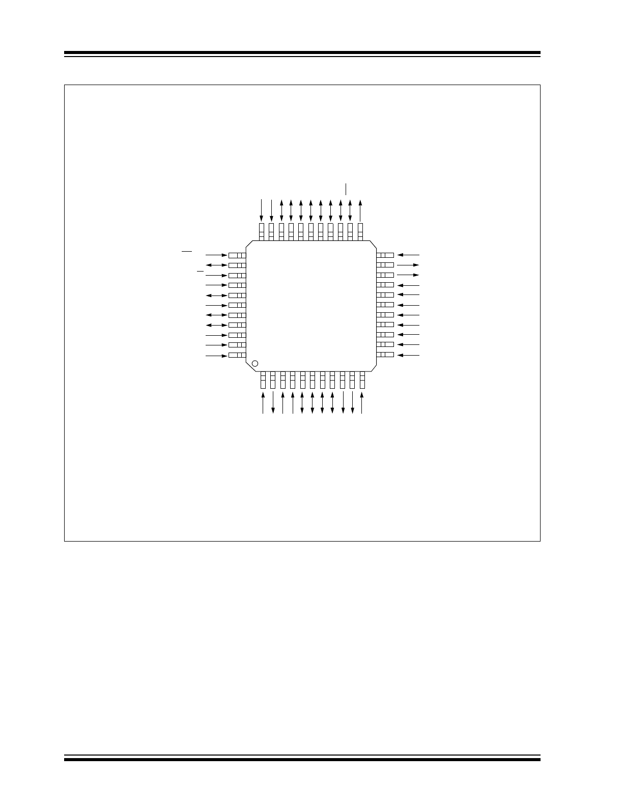
Pin Diagrams (Continued)
1 2 3 4 5 6 7 8 9 10 11 12 13 14 15 16
48 47 46 45 44 43 42 41 40 39 38 37 36 35 34 33
64
63
62
61
60
59
58
57
56
55
54
53
52
51
50
49
17
18
19
20
21
22
23
24
25
26
27
28
29
30
31
32
ENC624J600
A1
2
PSPCFG2
A1
4/
PSPCF
G
1
A1
3
A11
A10
A9
A8
A7
A5
A4
A3
A2
A1
WRH/
B
1
SE
L
A6
A0
PSPCFG3
AD7
AD6
AD5
AD4
OS
C1
OS
C2
V
SSOSC
V
DDO
S
C
CL
KOUT
LE
D
B
LE
D
A
AD1
1
AD1
0
AD9
AD8
TPIN-
V
SSTX
V
DDTX
TPOUT-
TPOUT+
V
SSTX
V
SS
AD1
5
AD1
4
AD1
3
AD1
2
V
SSRX
RBIAS
V
DDPLL
V
DDRX
V
SSPLL
IN
T
/SPI
SEL
CS/CS
SO/WR/WRL/EN/B0SEL
SI/RD/RW
SCK/AL/PSPCFG4
AD0
AD1
AD2
V
DD
V
CAP
V
SS
AD3
V
DD
V
DD
TPIN+
64-Pin TQFP

ENC424J600/624J600
DS39935C-page 4
2010 Microchip Technology Inc.
Table of Contents
1.0
Device Overview .......................................................................................................................................................................... 5
2.0
External Connections ................................................................................................................................................................... 9
3.0
Memory Organization ................................................................................................................................................................. 17
4.0
Serial Peripheral Interface (SPI)................................................................................................................................................. 39
5.0
Parallel Slave Port Interface (PSP) ............................................................................................................................................ 51
6.0
Ethernet Overview...................................................................................................................................................................... 71
7.0
Reset .......................................................................................................................................................................................... 73
8.0
Initialization................................................................................................................................................................................. 75
9.0
Transmitting and Receiving Packets .......................................................................................................................................... 83
10.0 Receive Filters............................................................................................................................................................................ 95
11.0 Flow Control ............................................................................................................................................................................. 105
12.0 Speed/Duplex Configuration and Auto-Negotiation.................................................................................................................. 109
13.0 Interrupts .................................................................................................................................................................................. 117
14.0 Direct Memory Access (DMA) Controller ................................................................................................................................. 123
15.0 Cryptographic Security Engines ............................................................................................................................................... 125
16.0 Power-Saving Features............................................................................................................................................................ 137
17.0 Electrical Characteristics .......................................................................................................................................................... 141
18.0 Packaging Information.............................................................................................................................................................. 149
Appendix A: Revision History............................................................................................................................................................. 157
Index .................................................................................................................................................................................................. 159
The Microchip Web Site ..................................................................................................................................................................... 163
Customer Change Notification Service .............................................................................................................................................. 163
Customer Support .............................................................................................................................................................................. 163
Reader Response .............................................................................................................................................................................. 164
Product Identification System............................................................................................................................................................. 165
TO OUR VALUED CUSTOMERS
It is our intention to provide our valued customers with the best documentation possible to ensure successful use of your Microchip
products. To this end, we will continue to improve our publications to better suit your needs. Our publications will be refined and
enhanced as new volumes and updates are introduced.
If you have any questions or comments regarding this publication, please contact the Marketing Communications Department via
E-mail at docerrors@microchip.com or fax the Reader Response Form in the back of this data sheet to (480) 792-4150. We
welcome your feedback.
Most Current Data Sheet
To obtain the most up-to-date version of this data sheet, please register at our Worldwide Web site at:
http://www.microchip.com
You can determine the version of a data sheet by examining its literature number found on the bottom outside corner of any page.
The last character of the literature number is the version number, (e.g., DS30000A is version A of document DS30000).
Errata
An errata sheet, describing minor operational differences from the data sheet and recommended workarounds, may exist for current
devices. As device/documentation issues become known to us, we will publish an errata sheet. The errata will specify the revision
of silicon and revision of document to which it applies.
To determine if an errata sheet exists for a particular device, please check with one of the following:
• Microchip’s Worldwide Web site; http://www.microchip.com
• Your local Microchip sales office (see last page)
When contacting a sales office, please specify which device, revision of silicon and data sheet (include literature number) you are
using.
Customer Notification System
Register on our web site at www.microchip.com to receive the most current information on all of our products.
2010 Microchip Technology Inc.
DS39935C-page 5
ENC424J600/624J600
1.0
DEVICE OVERVIEW
This document contains device-specific information for
the following devices:
• ENC424J600
• ENC624J600
The ENC424J600 and ENC624J600 are stand-alone,
Fast Ethernet controllers with an industry standard
Serial Peripheral Interface (SPI) or a flexible parallel
interface. They are designed to serve as an Ethernet
network interface for any microcontroller equipped with
SPI or a standard parallel port.
ENC424J600/624J600 devices meet all of the
IEEE 802.3 specifications applicable to 10Base-T and
100Base-TX Ethernet, including many optional
clauses, such as auto-negotiation. They incorporate a
number of packet filtering schemes to limit incoming
packets. They also provide an internal, 16-bit wide
DMA for fast data throughput and support for hardware
IP checksum calculations.
For applications that require the security and authenti-
cation features of SSL, TLS and other protocols related
to cryptography, a block of security engines is provided.
The engines perform RSA, Diffie-Hellman, AES, MD5
and SHA-1 algorithm computations, allowing reduced
code size, faster connection establishment and
throughput, and reduced firmware development effort.
Communication with the microcontroller is
implemented via the SPI or parallel interface, with data
rates ranging from 14 Mbit/s (SPI) to 160 Mbit/s
(demultiplexed, 16-bit parallel interface). Dedicated
pins are used for LED link and activity indication and for
transmit/receive/DMA interrupts.
A generous 24-Kbyte on-chip RAM buffer is available
for TX and RX operations. It may also be used by the
host microcontroller for general purpose storage.
Communication protocols, such as TCP, can use this
memory for saving data which may need to be
retransmitted.
For easy end product manufacturability, each
ENC624J600 family device is preprogrammed with a
unique nonvolatile MAC address. In most cases, this
allows the end device to avoid a serialized
programming step.
The only functional difference between the
ENC424J600 (44-pin) and ENC624J600 (64-pin)
devices are the number of parallel interface options
they support. These differences, along with a summary
of their common features, are provided in Table 1-1. A
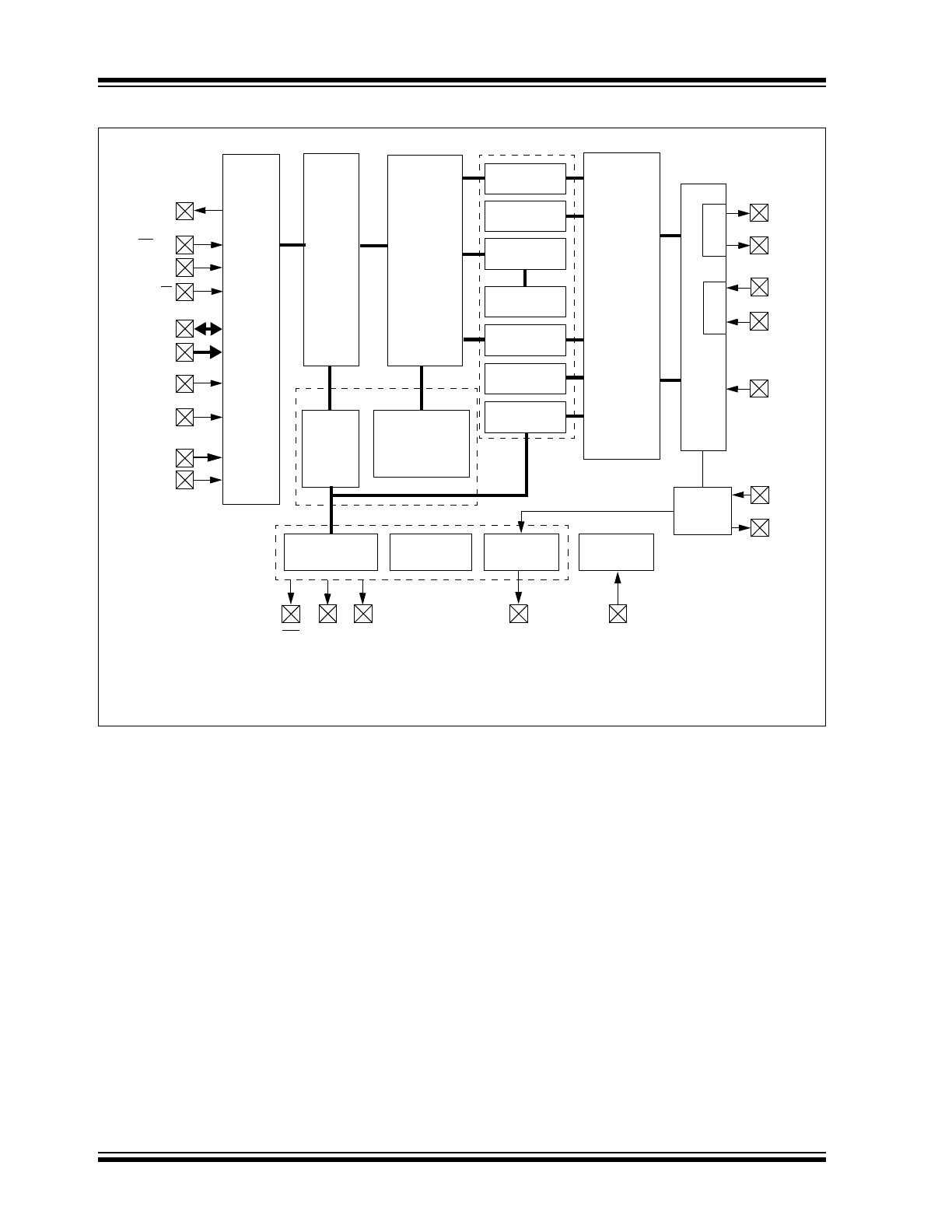
general block diagram for the devices is shown in
Figure 1-1.
A list of the pin features, sorted by function, is
presented in Table 1-2.
TABLE 1-1:
DEVICE FEATURES FOR ENC424J600/624J600
Feature
ENC424J600
ENC624J600
Pin Count
44
64
Ethernet Operating Speed
10/100 Mbps (auto-negotiate, auto-sense or manual)
Ethernet Duplex Modes
Half and Full (auto-negotiate and manual)
Ethernet Flow Control
Pause and Backpressure (auto and manual)
Buffer Memory (bytes)
24K (organized as 12K word x 16)
Internal Interrupt Sources
11 (mappable to a single external interrupt flag)
Serial Host Interface (SPI)
Yes
Yes
Parallel Host Interface:
Operating
modes
2
8
Muliplexed, 8-bit
Yes
Yes
16-bit
No
Yes
Demultiplexed, 8-bit
No
Yes
16-bit
No
Yes
Cryptographic Security Options:
AES, 128/192/256-bit
Yes
Yes
MD5/SHA-1
Yes
Yes
Modular Exponentiation, 1024-bit
Yes
Yes
Receive Filter Options
Accept or reject packets with CRC match/mismatch, runt error collect
or reject, Unicast, Not-Me Unicast, Multicast, Broadcast,
Magic Packet™, Pattern Table and Hash Table
Packages
44-Pin TQFP, QFN
64-Pin TQFP
ENC424J600/624J600
DS39935C-page 6
2010 Microchip Technology Inc.
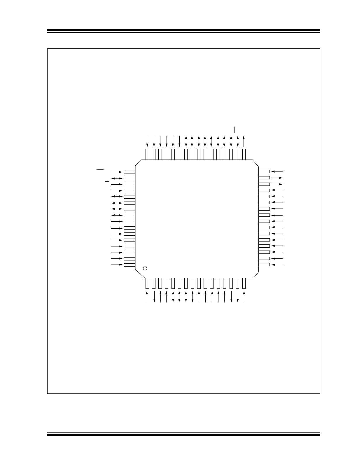
FIGURE 1-1:
ENC424J600/624J600 BLOCK DIAGRAM
24 Kbytes
DMA and
Checksum
TX Control
RX Control
Arbiter
Flow Control
Host Interface
Control
Registers
25 MHz
Power-on
PHY
MII
Interface
MIIM
Interface
TPOUT+
TPOUT-
TPIN+
TPIN-
TX
RX
RBIAS
OSC1
OSC2
Control Logic
CS/CS
SI/RD/RW
SO
SCK/AL
INT
V
CAP
CLKOUT
LEDA LEDB
RX Filter
MAC
m3
m1
SRAM
Note 1:
A<14:0>, AD15, WRL/B0SEL, WRH/B1SEL and PSPCFG<4:1> are available on 64-pin devices only. PSPCFG0 is available on 44-pin
devices only.
Reset
Oscillator
I/O
Interface
AD<15:0>
(1)
A<14:0>
(1)
Logic
Logic
Crypto Cores
Memory
Bus
Interface
SP
I
P
a
ra
lle
l
C
o
m
mo
n
SPISEL
PSPCFGx
(1)
EN/B0SEL
(1)
WR/WRL/
WRH/
B1SEL
(1)
m0
m2
PLL
Voltage
Regulator

2010 Microchip Technology Inc.
DS39935C-page 7
ENC424J600/624J600
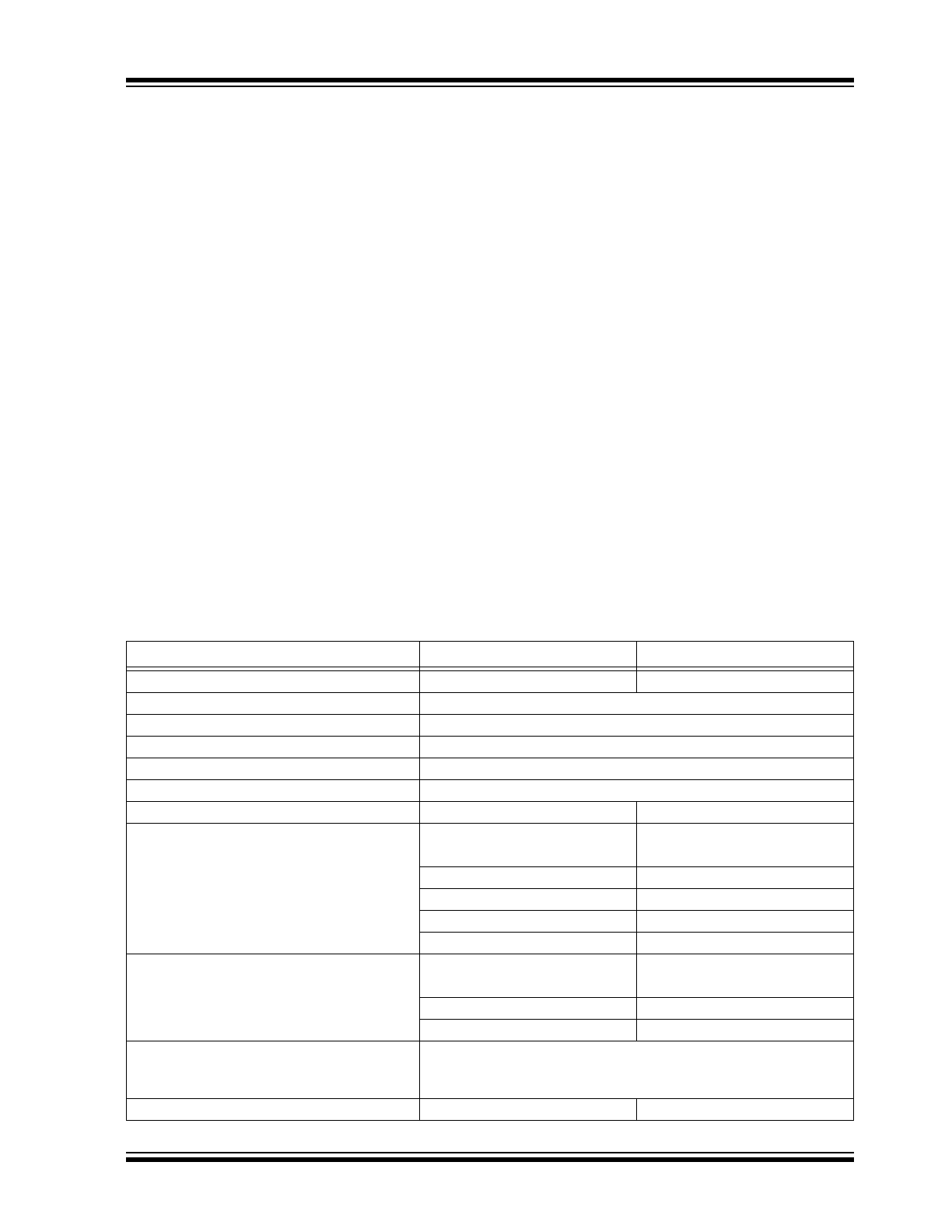
TABLE 1-2:
ENC424J600/624J600 PINOUT DESCRIPTIONS
Pin Name
Pin Number
Pin Type
Input
Buffer
Description
44-Pin
64-Pin
AD0
38
53
I/O
CMOS
PSP Multiplexed Address Input and/or Bidirectional
Data Bus
AD1
39
54
I/O
CMOS
AD2
40
55
I/O
CMOS
AD3
41
56
I/O
CMOS
AD4
5
5
I/O
CMOS
AD5
6
6
I/O
CMOS
AD6
7
7
I/O
CMOS
AD7
8
8
I/O
CMOS
AD8
25
35
I/O
CMOS
AD9
26
36
I/O
CMOS
AD10
27
37
I/O
CMOS
AD11
28
38
I/O
CMOS
AD12
29
39
I/O
CMOS
AD13
30
40
I/O
CMOS
AD14
31
41
I/O
CMOS
AD15
—
42
I/O
CMOS
A0
—
57
I
CMOS
PSP Demultiplexed Address Input Bus
A1
—
58
I
CMOS
A2
—
59
I
CMOS
A3
—
60
I
CMOS
A4
—
61
I
CMOS
A5
—
9
I
CMOS
A6
—
10
I
CMOS
A7
—
11
I
CMOS
A8
—
12
I
CMOS
A9
—
13
I
CMOS
A10
—
19
I
CMOS
A11
—
20
I
CMOS
A12
—
43
I
CMOS
A13
—
44
I
CMOS
A14
—
45
I
CMOS
AL
37
52
I
CMOS
PSP Address Latch
B0SEL
—
50
I
CMOS
PSP Byte 0 Select
B1SEL
—
48
I
CMOS
PSP Byte 1 Select
CLKOUT
23
33
O
—
Programmable Clock Output for External Use
CS
34
49
I
CMOS
SPI Chip Select (active-low)
CS
34
49
I
CMOS
PSP Chip Select (active-high)
EN
35
50
I
CMOS
PSP R/W Enable strobe
INT
24
34
O
—
Interrupt Output (active-low)
LEDA
10
15
O
—
Programmable Ethernet Status/Activity LED
LEDB
9
14
O
—
Programmable Ethernet Status/Activity LED
Legend: I = Input; O = Output; P = Power; CMOS = CMOS compatible input buffer; ANA = Analog level input/output

ENC424J600/624J600
DS39935C-page 8
2010 Microchip Technology Inc.
OSC1
3
3
I
ANA
25 MHz Crystal Oscillator/Clock Input
OSC2
2
2
O
—
25 MHz Crystal Oscillator Output
PSPCFG0
32
—
I
CMOS
PSP Mode Select 0
PSPCFG1
—
45
I
CMOS
PSP Mode Select 1
PSPCFG2
—
17
I
CMOS
PSP Mode Select 2
PSPCFG3
—
18
I
CMOS
PSP Mode Select 3
PSPCFG4
—
52
I
CMOS
PSP Mode Select 4
RBIAS
11
16
I
ANA
PHY Bias (external resistor) Connection
RD
36
51
I
CMOS
PSP Read Strobe
RW
36
51
I
CMOS
PSP Combined Read/Write Signal
SCK
37
52
I
CMOS
SPI Serial Clock Input
SI
36
51
I
CMOS
SPI Serial Data Input (from Master)
SO
35
50
O
—
SPI Serial Data Out (to Master)
SPISEL
24
34
I
CMOS
SPI/PSP Interface Select
TPIN-
17
27
I
ANA
Differential Ethernet Receive Minus Signal Input
TPIN+
16
26
I
ANA
Differential Ethernet Receive Plus Signal Input
TPOUT-
21
31
O
—
Differential Ethernet Transmit Minus Signal Output
TPOUT+
20
30
O
—
Differential Ethernet Transmit Plus Signal Output
V
CAP
43
63
P
—
Regulator External Capacitor connection
V
DD
44
21, 47,
64
P
—
Positive 3.3V Power Supply for Digital Logic
V
DDOSC
4
4
P
—
Positive 3.3V Power Supply for 25 MHz Oscillator
V
DDPLL
12
22
P
—
Positive 3.3V Power Supply for PHY PLL Circuitry
V
DDRX
15
25
P
—
Positive 3.3V Power Supply for PHY RX Circuitry
V
DDTX
18
28
P
—
Positive 3.3V Power Supply for PHY TX Circuitry
V
SS
33, 42
46, 62
P
—
Ground Reference for Digital Logic
V
SSOSC
1
1
P
—
Ground Reference for 25 MHz Oscillator
V
SSPLL
13
23
P
—
Ground Reference for PHY PLL Circuitry
V
SSRX
14
24
P
—
Ground Reference for PHY RX Circuitry
V
SSTX
19, 22
29, 32
P
—
Ground Reference for PHY TX Circuitry
WR
35
50
I
CMOS
PSP Write Strobe
WRH
—
48
I
CMOS
PSP Write High Strobe
WRL
—
50
I
CMOS
PSP Write Low Strobe
TABLE 1-2:
ENC424J600/624J600 PINOUT DESCRIPTIONS (CONTINUED)
Pin Name
Pin Number
Pin Type
Input
Buffer
Description
44-Pin
64-Pin
Legend: I = Input; O = Output; P = Power; CMOS = CMOS compatible input buffer; ANA = Analog level input/output