
2006-2012 Microchip Technology Inc.
.
DS39662E-page 1
ENC28J60
Ethernet Controller Features
• IEEE 802.3™ Compatible Ethernet Controller
• Fully Compatible with 10/100/1000Base-T Networks
• Integrated MAC and 10Base-T PHY
• Supports One 10Base-T Port with Automatic
Polarity Detection and Correction
• Supports Full and Half-Duplex modes
• Programmable Automatic Retransmit on Collision
• Programmable Padding and CRC Generation
• Programmable Automatic Rejection of Erroneous
Packets
• SPI Interface with Clock Speeds up to 20 MHz
Buffer
• 8-Kbyte Transmit/Receive Packet Dual Port SRAM
• Configurable Transmit/Receive Buffer Size
• Hardware Managed Circular Receive FIFO
• Byte-Wide Random and Sequential Access with
Auto-Increment
• Internal DMA for Fast Data Movement
• Hardware Assisted Checksum Calculation for
Various Network Protocols
Medium Access Controller (MAC)
Features
• Supports Unicast, Multicast and Broadcast
Packets
• Programmable Receive Packet Filtering and Wake-up
Host on Logical AND or OR of the Following:
- Unicast destination address
- Multicast address
- Broadcast address
- Magic Packet™
- Group destination addresses as defined by
64-bit Hash Table
- Programmable Pattern Matching of up to
64 bytes at user-defined offset
Physical Layer (PHY) Features
• Loopback mode
• Two Programmable LED Outputs for LINK, TX,
RX, Collision and Full/Half-Duplex Status
Operational
• Six Interrupt Sources and One Interrupt Output Pin
• 25 MHz Clock Input Requirement
• Clock Out Pin with Programmable Prescaler
• Operating Voltage of 3.1V to 3.6V (3.3V typical)
• 5V Tolerant Inputs
• Temperature Range: -40°C to +85°C Industrial,
0°C to +70°C Commercial (SSOP only)
• 28-Pin SPDIP, SSOP, SOIC, QFN Packages
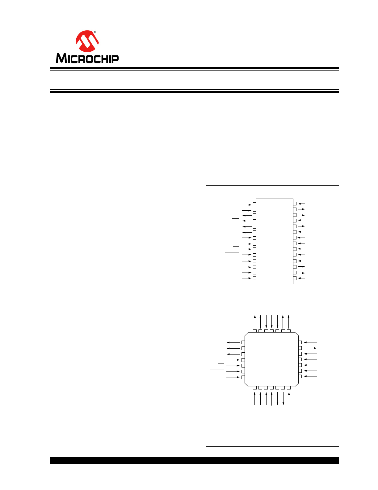
Package Types
E
N
C
2
8J
60
28-Pin SPDIP, SSOP, SOIC
1
2
3
4
5
6
7
8
9
10
11
12
13
14
15
16
17
18
19
20
21
22
23
24
25
26
27
28
OSC2
OSC1
LE
D
A
LE
D
B
TPI
N
+
TPI
N
-
INT
NC
(1)
1
2
3
4
5
6
7
8 9 10
28 27 26 25 24 23 22
21
20
19
ENC28J60
11 12 13 14
18
17
16
15
V
DDOSC
V
DD
T
X
TP
O
U
T+
TP
O
U
T
-
28-Pin QFN
(2)
RESET
CS
SO
SI
SCK
RBIAS
V
SSRX
CL
KOUT
V
CA
P
V
DDRX
V
SSOSC
V
DDPLL
V
SSPLL
V
SS
T
X
V
DD
V
SS
V
CAP
OSC2
OSC1
V
DDRX
V
SSTX
TPOUT+
TPOUT-
LEDA
LEDB
V
DDOSC
V
SSOSC
V
DDTX
V
DDPLL
V
SSPLL
CLKOUT
RESET
CS
SO
SI
TPIN+
TPIN-
RBIAS
INT
NC
(1)
SCK
V
DD
V
SS
V
SSRX
Note 1: Reserved pin; always leave disconnected.
2: The back pad on QFN devices should be connected
to Vss.
Stand-Alone Ethernet Controller with SPI Interface

ENC28J60
DS39662E-page 2
.
2006-2012 Microchip Technology Inc.
Table of Contents
1.0
Overview ...................................................................................................................................................................................... 3
2.0
External Connections ................................................................................................................................................................... 5
3.0
Memory Organization ................................................................................................................................................................. 11
4.0
Serial Peripheral Interface (SPI)................................................................................................................................................. 25
5.0
Ethernet Overview...................................................................................................................................................................... 31
6.0
Initialization................................................................................................................................................................................. 33
7.0
Transmitting and Receiving Packets .......................................................................................................................................... 39
8.0
Receive Filters............................................................................................................................................................................ 47
9.0
Duplex Mode Configuration and Negotiation.............................................................................................................................. 53
10.0 Flow Control ............................................................................................................................................................................... 55
11.0 Reset .......................................................................................................................................................................................... 59
12.0 Interrupts .................................................................................................................................................................................... 63
13.0 Direct Memory Access Controller ............................................................................................................................................... 71
14.0 Power-Down............................................................................................................................................................................... 73
15.0 Built-in Self-Test Controller ........................................................................................................................................................ 75
16.0 Electrical Characteristics ............................................................................................................................................................ 79
17.0 Packaging Information................................................................................................................................................................ 83
Appendix A: Revision History............................................................................................................................................................... 93
The Microchip Web Site ....................................................................................................................................................................... 95
Customer Change Notification Service ................................................................................................................................................ 95
Customer Support ................................................................................................................................................................................ 95
Reader Response ................................................................................................................................................................................ 96
Product Identification System............................................................................................................................................................... 99
TO OUR VALUED CUSTOMERS
It is our intention to provide our valued customers with the best documentation possible to ensure successful use of your Microchip
products. To this end, we will continue to improve our publications to better suit your needs. Our publications will be refined and
enhanced as new volumes and updates are introduced.
If you have any questions or comments regarding this publication, please contact the Marketing Communications Department via
E-mail at
docerrors@microchip.com
or fax the Reader Response Form in the back of this data sheet to (480) 792-4150. We
welcome your feedback.
Most Current Data Sheet
To obtain the most up-to-date version of this data sheet, please register at our Worldwide Web site at:
http://www.microchip.com
You can determine the version of a data sheet by examining its literature number found on the bottom outside corner of any page.
The last character of the literature number is the version number, (e.g., DS30000A is version A of document DS30000).
Errata
An errata sheet, describing minor operational differences from the data sheet and recommended workarounds, may exist for current
devices. As device/documentation issues become known to us, we will publish an errata sheet. The errata will specify the revision
of silicon and revision of document to which it applies.
To determine if an errata sheet exists for a particular device, please check with one of the following:
• Microchip’s Worldwide Web site;
http://www.microchip.com
• Your local Microchip sales office (see last page)
When contacting a sales office, please specify which device, revision of silicon and data sheet (include literature number) you are
using.
Customer Notification System
Register on our web site at
www.microchip.com
to receive the most current information on all of our products.
2006-2012 Microchip Technology Inc.
.
DS39662E-page 3
ENC28J60
1.0
OVERVIEW
The ENC28J60 is a stand-alone Ethernet controller
with an industry standard Serial Peripheral Interface
(SPI). It is designed to serve as an Ethernet network
interface for any controller equipped with SPI.
The ENC28J60 meets all of the IEEE 802.3 specifica-
tions. It incorporates a number of packet filtering
schemes to limit incoming packets. It also provides an
internal DMA module for fast data throughput and hard-
ware assisted checksum calculation, which is used in
various network protocols. Communication with the
host controller is implemented via an interrupt pin and
the SPI, with clock rates of up to 20 MHz. Two
dedicated pins are used for LED link and network
activity indication.
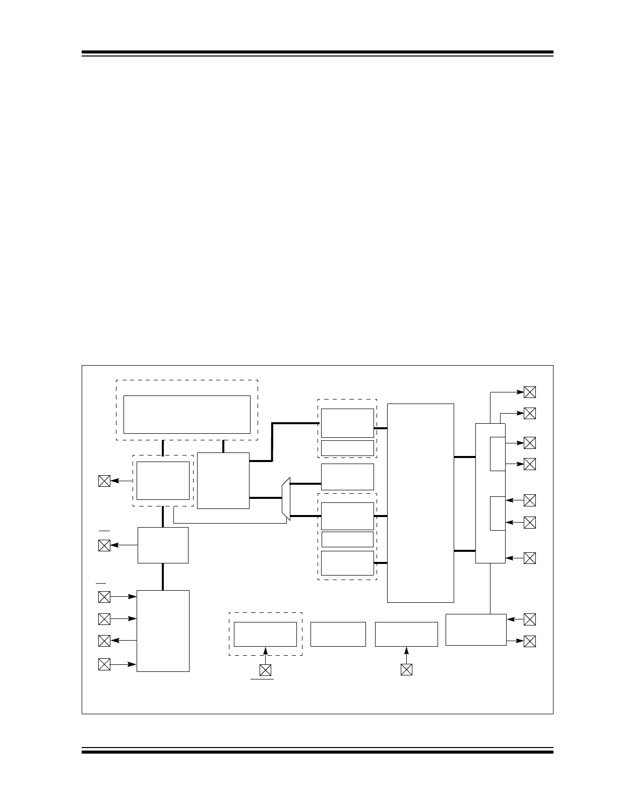
A simple block diagram of the ENC28J60 is shown in
Figure 1-1
. A typical application circuit using the device
is shown in
Figure 1-2
. With the ENC28J60, two pulse
transformers and a few passive components are all that
are required to connect a microcontroller to an Ethernet
network.
The ENC28J60 consists of seven major functional
blocks:
1.
An SPI interface that serves as a communica-
tion channel between the host controller and the
ENC28J60.
2.
Control registers which are used to control and
monitor the ENC28J60.
3.
A dual port RAM buffer for received and
transmitted data packets.
4.
An arbiter to control the access to the RAM buf-
fer when requests are made from DMA, transmit
and receive blocks.
5.
The bus interface that interprets data and
commands received via the SPI interface.
6.
The MAC (Medium Access Control) module that
implements IEEE 802.3 compliant MAC logic.
7.
The PHY (Physical Layer) module that encodes
and decodes the analog data that is present on
the twisted-pair interface.
The device also contains other support blocks, such as
the oscillator, on-chip voltage regulator, level translators
to provide 5V tolerant I/Os and system control logic.
FIGURE 1-1:
ENC28J60 BLOCK DIAGRAM
Dual Port RAM
8 Kbytes
DMA &
Checksum
TXBM
RXBM
Arbiter
Flow Control
Host Interface
Control
Registers
Power-on
PHY
Bus Interface
SPI
MII
Interface
MIIM
Interface
TPOUT+
TPOUT-
TPIN+
TPIN-
TX
RX
RBIAS
OSC1
OSC2
Voltage
System Control
CS
(1)
SI
(1)
SO
SCK
(1)
INT
V
CAP
CLKOUT
LEDA
LEDB
RESET
(1)
RXF (Filter)
RX
TX
MAC
ch0
ch1
ch0
ch1
Buffer
Note 1:
These pins are 5V tolerant.
Regulator
Reset
25 MHz
Oscillator
ENC28J60
DS39662E-page 4
.
2006-2012 Microchip Technology Inc.
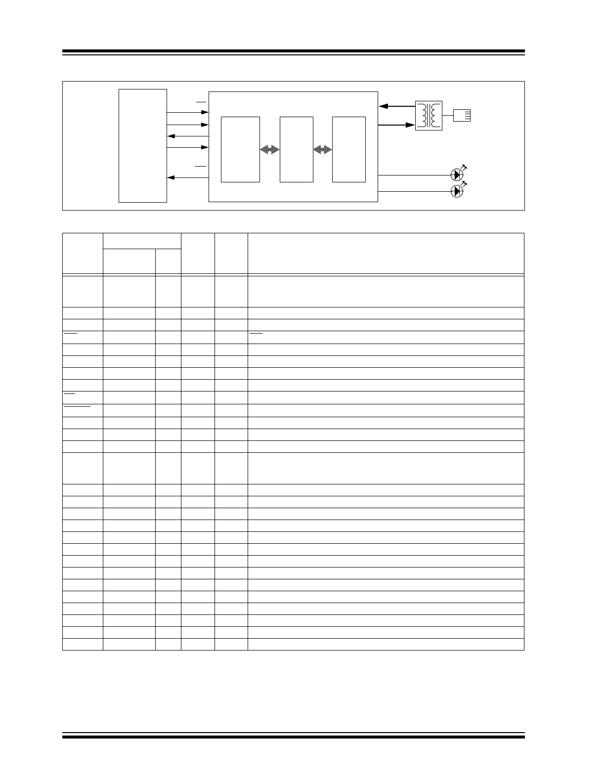
FIGURE 1-2:
TYPICAL ENC28J60 BASED INTERFACE
TABLE 1-1:
PINOUT I/O DESCRIPTIONS
Pin Name
Pin Number
Pin
Type
Buffer
Type
Description
SPDIP,
SOIC, SSOP
QFN
V
CAP
1
25
P
—
2.5V output from internal regulator. A low Equivalent Series Resistance (ESR)
capacitor, with a typical value of 10 µF and a minimum value of 1 µF to ground,
must be placed on this pin.
V
SS
2
26
P
—
Ground reference.
CLKOUT
3
27
O
—
Programmable clock output pin.
(
1
)
INT
4
28
O
—
INT interrupt output pin.
(
2
)
NC
5
1
O
—
Reserved function; always leave unconnected.
SO
6
2
O
—
Data out pin for SPI interface.
(
2
)
SI
7
3
I
ST
Data in pin for SPI interface.
(
3
)
SCK
8
4
I
ST
Clock in pin for SPI interface.
(
3
)
CS
9
5
I
ST
Chip select input pin for SPI interface.
(
3
,
4
)
RESET
10
6
I
ST
Active-low device Reset input.
(
3
,
4
)
V
SSRX
11
7
P
—
Ground reference for PHY RX.
TPIN-
12
8
I
ANA
Differential signal input.
TPIN+
13
9
I
ANA
Differential signal input.
RBIAS
14
10
I
ANA
Bias current pin for PHY. Must be tied to ground via a resistor (refer to
Section 2.4 “Magnetics, Termination and Other External Components”
for details).
V
DDTX
15
11
P
—
Positive supply for PHY TX.
TPOUT-
16
12
O
—
Differential signal output.
TPOUT+
17
13
O
—
Differential signal output.
V
SSTX
18
14
P
—
Ground reference for PHY TX.
V
DDRX
19
15
P
—
Positive 3.3V supply for PHY RX.
V
DDPLL
20
16
P
—
Positive 3.3V supply for PHY PLL.
V
SSPLL
21
17
P
—
Ground reference for PHY PLL.
V
SSOSC
22
18
P
—
Ground reference for oscillator.
OSC1
23
19
I
ANA
Oscillator input.
OSC2
24
20
O
—
Oscillator output.
V
DDOSC
25
21
P
—
Positive 3.3V supply for oscillator.
LEDB
26
22
O
—
LEDB driver pin.
(
5
)
LEDA
27
23
O
—
LEDA driver pin.
(
5
)
V
DD
28
24
P
—
Positive 3.3V supply.
Legend:
I = Input, O = Output, P = Power, ANA = Analog Signal Input, ST = Schmitt Trigger
Note 1:
Pins have a maximum current capacity of 8 mA.
2:
Pins have a maximum current capacity of 4 mA.
3:
Pins are 5V tolerant.
4:
Pins have an internal weak pull-up to V
DD
.
5:
Pins have a maximum current capacity of 12 mA.
TRANSFORMER
MCU
TX/RX
Buffer
MAC
PHY
LEDA
LEDB
SI
SO
SCK
INT
SDO
SDI
SCK
INT
X
ENC28J60
TPIN+/-
TPOUT+/-
ETHERNET
RJ45
I/O
CS
2006-2012 Microchip Technology Inc.
.
DS39662E-page 5
ENC28J60
2.0
EXTERNAL CONNECTIONS
2.1
Oscillator
The ENC28J60 is designed to operate at 25 MHz with a
crystal connected to the OSC1 and OSC2 pins. The
ENC28J60 design requires the use of a parallel reso-
nance crystal. Use of a series resonance crystal may give
a frequency out of the crystal manufacturer specifications.
A typical oscillator circuit is shown in
Figure 2-1
.
The ENC28J60 may also be driven by an external clock
source connected to the OSC1 pin as shown in
Figure 2-2
.
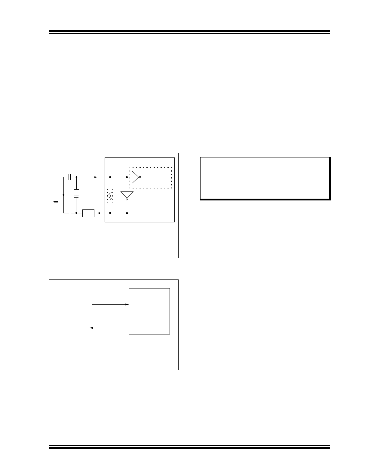
FIGURE 2-1:
CRYSTAL OSCILLATOR
OPERATION
FIGURE 2-2:
EXTERNAL CLOCK
SOURCE
(1)
2.2
Oscillator Start-up Timer
The ENC28J60 contains an Oscillator Start-up Timer
(OST) to ensure that the oscillator and integrated PHY
have stabilized before use. The OST does not expire
until 7500 OSC1 clock cycles (300
s) pass after
Power-on Reset or wake-up from Power-Down mode
occurs. During the delay, all Ethernet registers and buf-
fer memory may still be read and written to through the
SPI bus. However, software should not attempt to
transmit any packets (set ECON1.TXRTS), enable
reception of packets (set ECON1.RXEN) or access any
MAC, MII or PHY registers during this period.
When the OST expires, the CLKRDY bit in the ESTAT
register will be set. The application software should poll
this bit as necessary to determine when normal device
operation can begin.
C
1
C
2
XTAL
OSC2
R
S(1)
OSC1
R
F(2)
To Internal Logic
Note 1: A series resistor, R
S
, may be required for AT
strip cut crystals.
2: The feedback resistor, R
F
, is typically in the
range of 2 to 10 M
.
ENC28J60
3.3V Clock from
External System
OSC1
OSC2
Open
(2)
Note 1: Duty cycle restrictions must be observed.
2: A resistor to ground may be used to reduce
system noise. This may increase system
current.
ENC28J60
Note:
After a Power-on Reset, or the ENC28J60
is removed from Power-Down mode, the
CLKRDY bit must be polled before
transmitting packets, enabling packet
reception or accessing any MAC, MII or
PHY registers.
ENC28J60
DS39662E-page 6
.
2006-2012 Microchip Technology Inc.
2.3
CLKOUT Pin
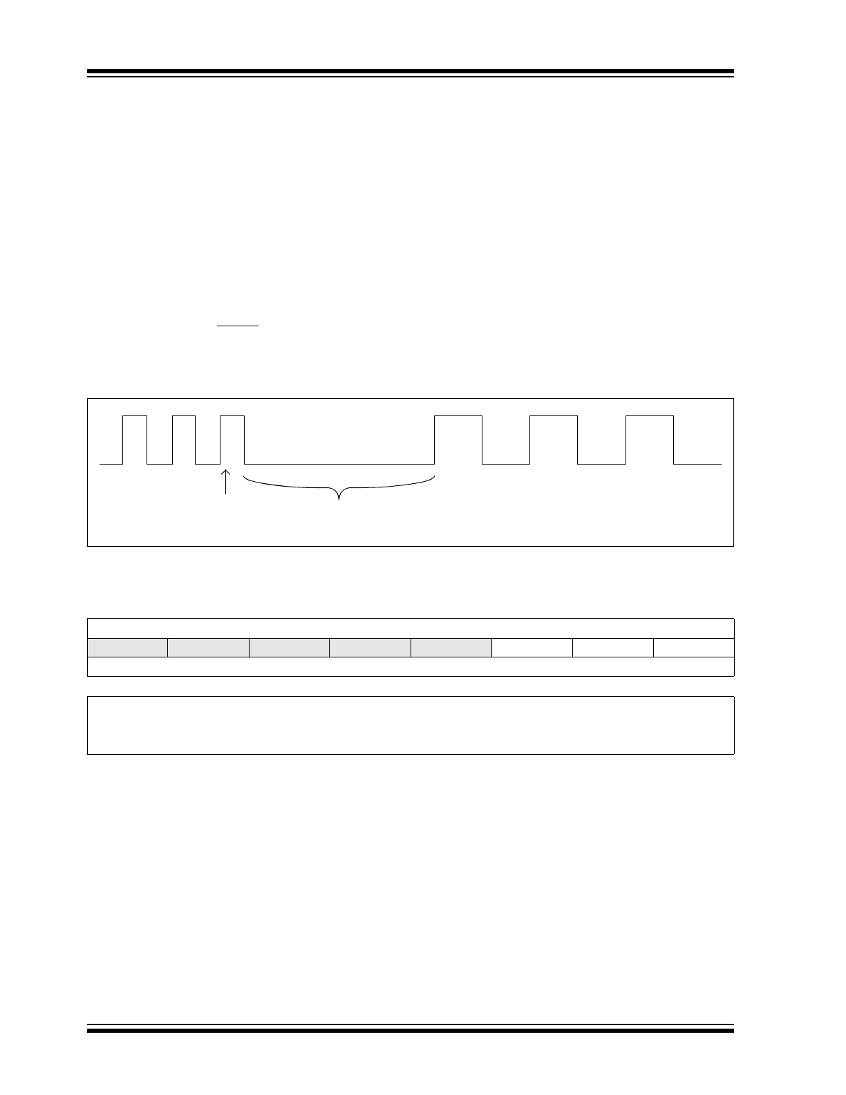
The Clock Out (CLKOUT) pin is provided to the system
designer for use as the host controller clock or as a
clock source for other devices in the system. The
CLKOUT has an internal prescaler which can divide the
output by 1, 2, 3, 4 or 8. The CLKOUT function is
enabled and the prescaler is selected via the ECOCON
register (
Register 2-1
).
To create a clean clock signal, the CLKOUT pin is held
low for a period when power is first applied. After the
Power-on Reset ends, the OST will begin counting.
When the OST expires, the CLKOUT pin will begin out-
putting its default frequency of 6.25 MHz (main clock
divided by 4). At any future time that the ENC28J60 is
reset by software or the RESET pin, the CLKOUT func-
tion will not be altered (ECOCON will not change
value). Additionally, Power-Down mode may be
entered and the CLKOUT function will continue to
operate. When Power-Down mode is cancelled, the
OST will be reset but the CLKOUT function will
continue. When the CLKOUT function is disabled
(ECOCON = 0), the CLKOUT pin is driven low.
The CLKOUT function is designed to ensure that mini-
mum timings are preserved when the CLKOUT pin
function is enabled, disabled or the prescaler value is
changed. No high or low pulses will be outputted which
exceed the frequency specified by the ECOCON
configuration. However, when switching frequencies, a
delay between two and eight OSC1 clock periods will
occur where no clock pulses will be produced (see
Figure 2-3
). During this period, CLKOUT will be held
low.
FIGURE 2-3:
CLKOUT TRANSITION
ECOCON
Changed
80 ns to 320 ns Delay
REGISTER 2-1:
ECOCON: CLOCK OUTPUT CONTROL REGISTER
U-0
U-0
U-0
U-0
U-0
R/W-1
R/W-0
R/W-0
—
—
—
—
—
COCON2
COCON1
COCON0
bit 7
bit 0
Legend:
R = Readable bit
W = Writable bit
U = Unimplemented bit, read as ‘0’
-n = Value at POR
‘1’ = Bit is set
‘0’ = Bit is cleared
x = Bit is unknown
bit 7-3
Unimplemented: Read as ‘0’
bit 2-0
COCON<2:0>: Clock Output Configuration bits
11x = Reserved for factory test, do not use; glitch prevention is not assured
101 = CLKOUT outputs main clock divided by 8 (3.125 MHz)
100 = CLKOUT outputs main clock divided by 4 (6.25 MHz)
011 = CLKOUT outputs main clock divided by 3 (8.333333 MHz)
010 = CLKOUT outputs main clock divided by 2 (12.5 MHz)
001 = CLKOUT outputs main clock divided by 1 (25 MHz)
000 = CLKOUT is disabled, the pin is driven low
2006-2012 Microchip Technology Inc.
.
DS39662E-page 7
ENC28J60
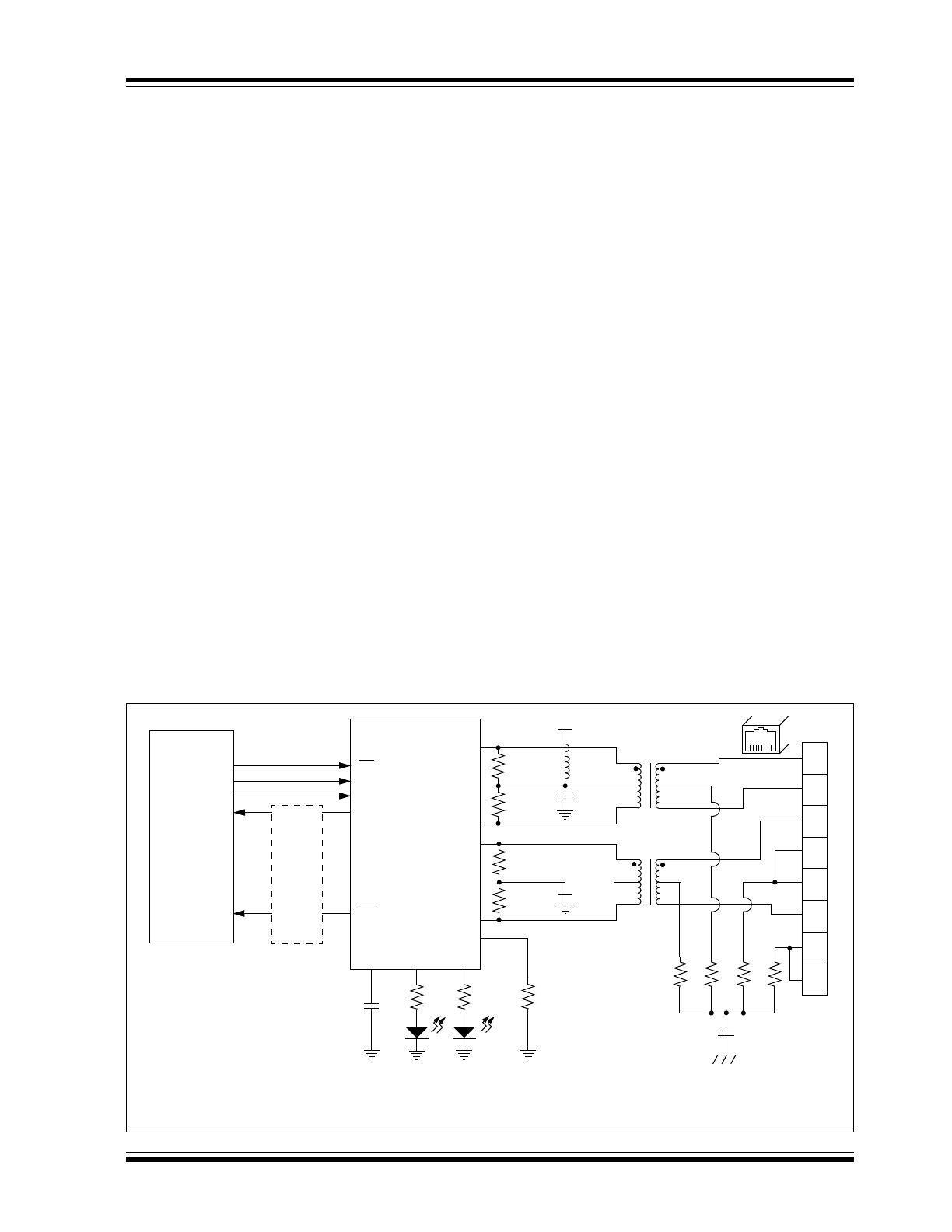
2.4
Magnetics, Termination and Other
External Components
To complete the Ethernet interface, the ENC28J60
requires several standard components to be installed
externally. These components should be connected as
shown in
Figure 2-4
.
The internal analog circuitry in the PHY module requires
that an external 2.32 k
, 1% resistor be attached from
RBIAS to ground. The resistor influences the TPOUT+/-
signal amplitude. The resistor should be placed as close
as possible to the chip with no immediately adjacent
signal traces to prevent noise capacitively coupling into
the pin and affecting the transmit behavior. It is
recommended that the resistor be a surface mount type.
Some of the device’s digital logic operates at a nominal
2.5V. An on-chip voltage regulator is incorporated to
generate this voltage. The only external component
required is an external filter capacitor, connected from
V
CAP
to ground. The capacitor must have low equiva-
lent series resistance (ESR), with a typical value of
10
F, and a minimum value of 1 F. The internal
regulator is not designed to drive external loads.
On the TPIN+/TPIN- and TPOUT+/TPOUT- pins,
1:1 center taped pulse transformers, rated for Ethernet
operations, are required. When the Ethernet module is
enabled, current is continually sunk through both
TPOUT pins. When the PHY is actively transmitting, a
differential voltage is created on the Ethernet cable by
varying the relative current sunk by TPOUT+ compared
to TPOUT-.
A common-mode choke on the TPOUT interface, placed
between the TPOUT pins and the Ethernet transformer
(not shown), is not recommended. If a common-mode
choke is used to reduce EMI emissions, it should be
placed between the Ethernet transformer and pins 1 and
2 of the RJ-45 connector. Many Ethernet transformer
modules include common-mode chokes inside the same
device package. The transformers should have at least
the isolation rating specified in
Table 16-5
to protect
against static voltages and meet IEEE 802.3 isolation
requirements (see
Section 16.0 “Electrical Character-
istics”
for specific transformer requirements). Both
transmit and receive interfaces additionally require two
resistors and a capacitor to properly terminate the
transmission line, minimizing signal reflections.
All power supply pins must be externally connected to
the same power source. Similarly, all ground refer-
ences must be externally connected to the same
ground node. Each V
DD
and V
SS
pin pair should have
a 0.1
F ceramic bypass capacitor (not shown in the
schematic) placed as close to the pins as possible.
Since relatively high currents are necessary to operate
the twisted-pair interface, all wires should be kept as
short as possible. Reasonable wire widths should be
used on power wires to reduce resistive loss. If the
differential data lines cannot be kept short, they should
be routed in such a way as to have a 100
characteristic
impedance.
FIGURE 2-4:
ENC28J60 ETHERNET TERMINATION AND EXTERNAL CONNECTIONS
I/O
SCK
SDO
SDI
INT0
MCU
Level
Shift
Logic
(2)
CS
SCK
SI
SO
INT
ENC28J60
V
CAP
LEDA
LEDB
RBIAS
TPOUT
+
TPOUT
-
TPIN
+
TPIN
-
10
F
Note 1:
Ferrite Bead should be rated for at least 80 mA.
2:
Required only if the microcontroller is operating at 5V. See
Section 2.5 “I/O Levels”
for more information.
3:
These components are installed for EMI reduction purposes.
Ferrite
Bead
(1,3)
3.3V
2.32 k
, 1%
1
2
3
4
5
6
7
8
RJ-45
1:1 CT
1:1 CT
1 nF, 2 kV
(3)
75
(3)
75
(3)
75
(3)
75
(3)
49.9
, 1%
49.9
, 1%
49.9
, 1%
49.9
, 1%
0.1
F
(3)
0.1
F
1
ENC28J60
DS39662E-page 8
.
2006-2012 Microchip Technology Inc.
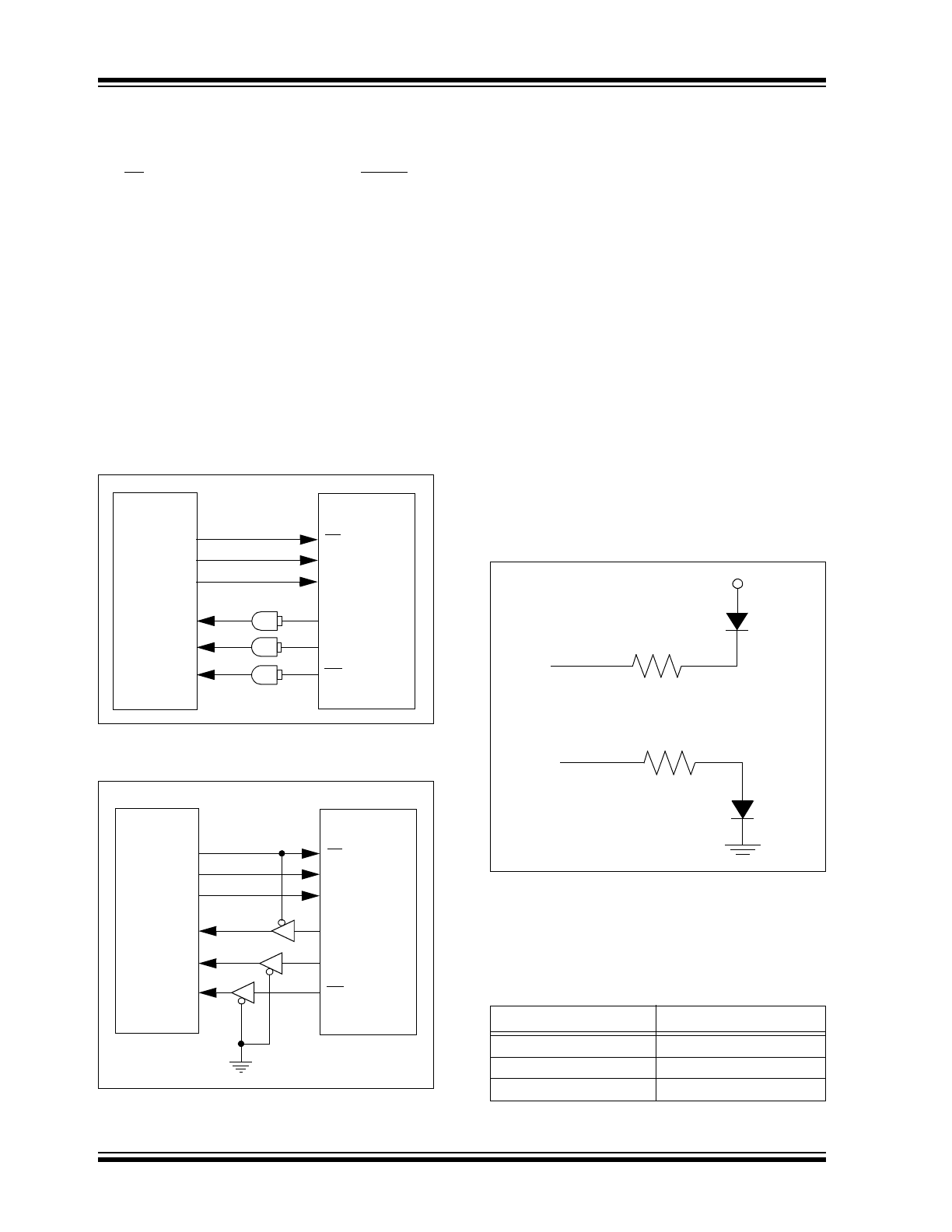
2.5
I/O Levels
The ENC28J60 is a 3.3V part; however, it was
designed to be easily integrated into 5V systems. The
SPI CS, SCK and SI inputs, as well as the RESET pin,
are all 5V tolerant. On the other hand, if the host
controller is operated at 5V, it quite likely will not be
within specifications when its SPI and interrupt inputs
are driven by the 3.3V CMOS outputs on the
ENC28J60. A unidirectional level translator would be
necessary.
An economical 74HCT08 (quad AND gate), 74ACT125
(quad 3-state buffer) or many other 5V CMOS chips
with TTL level input buffers may be used to provide the
necessary level shifting. The use of 3-state buffers
permits easy integration into systems which share the
SPI bus with other devices.
Figure 2-5
and
Figure 2-6
show example translation schemes.
FIGURE 2-5:
LEVEL SHIFTING USING
AND GATES
FIGURE 2-6:
LEVEL SHIFTING USING
3-STATE BUFFERS
2.6
LED Configuration
The LEDA and LEDB pins support automatic polarity
detection on Reset. The LEDs can be connected such
that the pin must source current to turn the LED on, or
alternately connected such that the pin must sink cur-
rent to turn the LED on. Upon system Reset, the
ENC28J60 will detect how the LED is connected and
begin driving the LED to the default state configured by
the PHLCON register. If the LED polarity is changed
while the ENC28J60 is operating, the new polarity will
not be detected until the next system Reset occurs.
LEDB is unique in that the connection of the LED is
automatically read on Reset and determines how to
initialize the PHCON1.PDPXMD bit. If the pin sources
current to illuminate the LED, the bit is cleared on
Reset and the PHY defaults to half-duplex operation. If
the pin sinks current to illuminate the LED, the bit is set
on Reset and the PHY defaults to full-duplex operation.
Figure 2-7
shows the two available options. If no LED
is attached to the LEDB pin, the PDPXMD bit will reset
to an indeterminate value.
FIGURE 2-7:
LEDB POLARITY AND
RESET CONFIGURATION
OPTIONS
The LEDs can also be configured separately to control
their operating polarity (on or off when active), blink rate
and blink stretch interval. The options are controlled by
the LACFG<3:0> and LBCFG<3:0> bits. Typical values
for blink stretch are listed in
Table 2-1
.
TABLE 2-1:
LED BLINK STRETCH LENGTH
I/O
SCK
SO
SI
INT0
MCU
CS
SCK
SI
SO
INT
ENC28J60
CLKOUT
OSC1
I/O
SCK
SO
SI
INT0
MCU
CS
SCK
SI
SO
INT
ENC28J60
CLKOUT
OSC1
Stretch Length
Typical Stretch (ms)
T
NSTRCH
(normal)
40
T
MSTRCH
(medium)
70
T
LSTRCH
(long)
140
LEDB
+3.3V
Full-Duplex Operation:
PDPXMD =
1
LEDB
Half-Duplex Operation:
PDPXMD =
0

2006-2012 Microchip Technology Inc.
.
DS39662E-page 9
ENC28J60
REGISTER 2-2:
PHLCON: PHY MODULE LED CONTROL REGISTER
R/W-0
R/W-0
R/W-1
R/W-1
R/W-0
R/W-1
R/W-0
R/W-0
r
r
r
r
LACFG3
LACFG2
LACFG1
LACFG0
bit 15
bit 8
R/W-0
R/W-0
R/W-1
R/W-0
R/W-0
R/W-0
R/W-1
R/W-x
LBCFG3
LBCFG2
LBCFG1
LBCFG0
LFRQ1
LFRQ0
STRCH
r
bit 7
bit 0
Legend:
r = Reserved bit
R = Readable bit
W = Writable bit
U = Unimplemented bit, read as ‘0’
-n = Value at POR
‘1’ = Bit is set
‘0’ = Bit is cleared
x = Bit is unknown
bit 15-14
Reserved: Write as ‘0’
bit 13-12
Reserved: Write as ‘1’
bit 11-8
LACFG<3:0>: LEDA Configuration bits
1111 = Reserved
1110 = Display duplex status and collision activity (always stretched)
1101 = Display link status and transmit/receive activity (always stretched)
1100 = Display link status and receive activity (always stretched)
1011 = Blink slow
1010 = Blink fast
1001 = Off
1000 = On
0111 = Display transmit and receive activity (stretchable)
0110 = Reserved
0101 = Display duplex status
0100 = Display link status
0011 = Display collision activity (stretchable)
0010 = Display receive activity (stretchable)
0001 = Display transmit activity (stretchable)
0000 = Reserved
bit 7-4
LBCFG<3:0>: LEDB Configuration bits
1110 = Display duplex status and collision activity (always stretched)
1101 = Display link status and transmit/receive activity (always stretched)
1100 = Display link status and receive activity (always stretched)
1011 = Blink slow
1010 = Blink fast
1001 = Off
1000 = On
0111 = Display transmit and receive activity (stretchable)
0110 = Reserved
0101 = Display duplex status
0100 = Display link status
0011 = Display collision activity (stretchable)
0010 = Display receive activity (stretchable)
0001 = Display transmit activity (stretchable)
0000 = Reserved
bit 3-2
LFRQ<1:0>: LED Pulse Stretch Time Configuration bits (see
Table 2-1
)
11 = Reserved
10 = Stretch LED events by T
LSTRCH
01 = Stretch LED events by T
MSTRCH
00 = Stretch LED events by T
NSTRCH
bit 1
STRCH: LED Pulse Stretching Enable bit
1 = Stretchable LED events will cause lengthened LED pulses based on LFRQ<1:0> configuration
0 = Stretchable LED events will only be displayed while they are occurring
bit 0
Reserved: Write as ‘0’

ENC28J60
DS39662E-page 10
.
2006-2012 Microchip Technology Inc.
NOTES: