
SMSC EMC1701
DATASHEET
Revision 1.2 (09-27-10)
Datasheet
PRODUCT FEATURES
EMC1701
High-Side Current-Sense and Internal
1°C Temperature Monitor
General Description
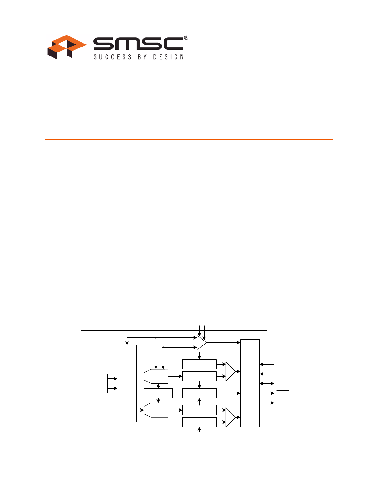
The EMC1701 is a combination high-side current sensing
device with precision temperature measurement. It
measures the voltage developed across an external sense
resistor to represent the high-side current of a battery or
voltage regulator. The EMC1701 also measures the source
voltage and uses these measured values to present a
proportional power calculation. The EMC1701 contains
additional bi-directional peak detection circuitry to flag
instantaneous current spikes with programmable time
duration and magnitude threshold. Finally, the EMC1701
includes an internal diode channel for ambient temperature
measurement.
Both current sensing and temperature monitoring include
two tiers of protection: one that can be masked and causes
the ALERT pin to be asserted, and the other that cannot be
masked and causes the THERM pin to be asserted.
Applications
Notebook and Desktop Computers
Industrial
Power Management Systems
Embedded Applications
Features
High-side current sensor
—
Bi-directional current measurement
—
Measures source voltage and indicates power ratio
—
1% current measurement accuracy
—
Integrated over 82ms to 2.6sec with 11-bit resolution
—
3V to 24V bus voltage range
Independent hardware set instantaneous current peak
detector (EMC1701-1 only)
—
Software controls to program time duration and
magnitude threshold
Power supply options
—
Bus or separately powered for low voltage operation
Wide temperature operating range: -40°C to +85°C
Internal temperature monitor
—
±1°C accuracy (-5°C < T
A
< 85°C)
ALERT and THERM outputs for temperature, voltage,
and out-of-current limit reporting
SMBus 2.0 interface
—
Pin-selectable SMBus Address
—
Block Read and Write
Available in a 12-pin 4mm x 4mm QFN RoHS Compliant
Package (EMC1701-1)
Available in a 10-pin MSOP RoHS Compliant Package
(EMC1701-2)
Block Diagram
Analog
Mux
Internal
Temp
Diode
SMBus
Slave
Protocol
SMCLK
SMDATA
ADDR_SEL
SE
NSE
+
SE
NSE
-
DU
R
_
S
E
L*
TH
_
SEL
*
Peak
Detection
Voltage and
Temp Registers
Configuration
11 - 15 bit
Σ Δ ADC
13 - 15 bit
Σ Δ ADC
Current Registers
Current Limits
Voltage and
Temp Limits
THERM
ALERT
Power Register
*EMC1701-1 only
REEL SIZE IS 4,000 PIECES
This product meets the halogen maximum concentration values per IEC61249-2-21
For RoHS compliance and environmental information, please visit
ORDERING NUMBER
PACKAGE
FEATURES
EMC1701-1-KP-TR
12-pin 4mm x 4mm QFN
(Lead-free RoHS compliant)
Internal diode, current sensor,
hardware set peak detector
EMC1701-2-AIZL-TR
10-pin MSOP
(Lead-free RoHS compliant)
Internal diode, current sensor
High-Side Current-Sense and Internal 1°C Temperature Monitor
Datasheet
Revision 1.2 (09-27-10)
2
SMSC EMC1701
DATASHEET
80 ARKAY DRIVE, HAUPPAUGE, NY 11788 (631) 435-6000, FAX (631) 273-3123
Copyright © 2010 SMSC or its subsidiaries. All rights reserved.
Circuit diagrams and other information relating to SMSC products are included as a means of illustrating typical applications. Consequently, complete information sufficient for
construction purposes is not necessarily given. Although the information has been checked and is believed to be accurate, no responsibility is assumed for inaccuracies. SMSC
reserves the right to make changes to specifications and product descriptions at any time without notice. Contact your local SMSC sales office to obtain the latest specifications
before placing your product order. The provision of this information does not convey to the purchaser of the described semiconductor devices any licenses under any patent
rights or other intellectual property rights of SMSC or others. All sales are expressly conditional on your agreement to the terms and conditions of the most recently dated
version of SMSC's standard Terms of Sale Agreement dated before the date of your order (the "Terms of Sale Agreement"). The product may contain design defects or errors
known as anomalies which may cause the product's functions to deviate from published specifications. Anomaly sheets are available upon request. SMSC products are not
designed, intended, authorized or warranted for use in any life support or other application where product failure could cause or contribute to personal injury or severe property
damage. Any and all such uses without prior written approval of an Officer of SMSC and further testing and/or modification will be fully at the risk of the customer. Copies of
this document or other SMSC literature, as well as the Terms of Sale Agreement, may be obtained by visiting SMSC’s website at http://www.smsc.com. SMSC is a registered
trademark of Standard Microsystems Corporation (“SMSC”). Product names and company names are the trademarks of their respective holders.
SMSC DISCLAIMS AND EXCLUDES ANY AND ALL WARRANTIES, INCLUDING WITHOUT LIMITATION ANY AND ALL IMPLIED WARRANTIES OF MERCHANTABILITY,
FITNESS FOR A PARTICULAR PURPOSE, TITLE, AND AGAINST INFRINGEMENT AND THE LIKE, AND ANY AND ALL WARRANTIES ARISING FROM ANY COURSE
OF DEALING OR USAGE OF TRADE. IN NO EVENT SHALL SMSC BE LIABLE FOR ANY DIRECT, INCIDENTAL, INDIRECT, SPECIAL, PUNITIVE, OR CONSEQUENTIAL
DAMAGES; OR FOR LOST DATA, PROFITS, SAVINGS OR REVENUES OF ANY KIND; REGARDLESS OF THE FORM OF ACTION, WHETHER BASED ON CONTRACT;
TORT; NEGLIGENCE OF SMSC OR OTHERS; STRICT LIABILITY; BREACH OF WARRANTY; OR OTHERWISE; WHETHER OR NOT ANY REMEDY OF BUYER IS HELD
TO HAVE FAILED OF ITS ESSENTIAL PURPOSE, AND WHETHER OR NOT SMSC HAS BEEN ADVISED OF THE POSSIBILITY OF SUCH DAMAGES.
Ordering Information:
High-Side Current-Sense and Internal 1°C Temperature Monitor
Datasheet
SMSC EMC1701
3
Revision 1.2 (09-27-10)
DATASHEET
Table of Contents
Chapter 1
Pin Description . . . . . . . . . . . . . . . . . . . . . . . . . . . . . . . . . . . . . . . . . . . . . . . . . . . . . 8
Chapter 2
Electrical Characteristics . . . . . . . . . . . . . . . . . . . . . . . . . . . . . . . . . . . . . . . . . . . 10
2.1
Electrical Specifications . . . . . . . . . . . . . . . . . . . . . . . . . . . . . . . . . . . . . . . . . . . . . . . . . . . . . . . . . 11
2.2
SMBus Electrical Specifications . . . . . . . . . . . . . . . . . . . . . . . . . . . . . . . . . . . . . . . . . . . . . . . . . . . 13
Chapter 3
Communications . . . . . . . . . . . . . . . . . . . . . . . . . . . . . . . . . . . . . . . . . . . . . . . . . . 15
3.1
System Management Bus Interface Protocol . . . . . . . . . . . . . . . . . . . . . . . . . . . . . . . . . . . . . . . . . 15
3.1.1
SMBus Start Bit . . . . . . . . . . . . . . . . . . . . . . . . . . . . . . . . . . . . . . . . . . . . . . . . . . . . . . . . 15
3.1.2
SMBus Address and RD / WR Bit . . . . . . . . . . . . . . . . . . . . . . . . . . . . . . . . . . . . . . . . . . 15
3.1.3
SMBus ACK and NACK Bits . . . . . . . . . . . . . . . . . . . . . . . . . . . . . . . . . . . . . . . . . . . . . . 16
3.1.4
SMBus Stop Bit . . . . . . . . . . . . . . . . . . . . . . . . . . . . . . . . . . . . . . . . . . . . . . . . . . . . . . . . 16
3.1.5
SMBus Time-out . . . . . . . . . . . . . . . . . . . . . . . . . . . . . . . . . . . . . . . . . . . . . . . . . . . . . . . 16
3.1.6
SMBus and I
2
C Compliance . . . . . . . . . . . . . . . . . . . . . . . . . . . . . . . . . . . . . . . . . . . . . . 16
3.2
SMBus Protocols . . . . . . . . . . . . . . . . . . . . . . . . . . . . . . . . . . . . . . . . . . . . . . . . . . . . . . . . . . . . . . 17
3.2.1
Write Byte . . . . . . . . . . . . . . . . . . . . . . . . . . . . . . . . . . . . . . . . . . . . . . . . . . . . . . . . . . . . 17
3.2.2
Read Byte . . . . . . . . . . . . . . . . . . . . . . . . . . . . . . . . . . . . . . . . . . . . . . . . . . . . . . . . . . . . 17
3.2.3
Send Byte . . . . . . . . . . . . . . . . . . . . . . . . . . . . . . . . . . . . . . . . . . . . . . . . . . . . . . . . . . . . 17
3.2.4
Receive Byte . . . . . . . . . . . . . . . . . . . . . . . . . . . . . . . . . . . . . . . . . . . . . . . . . . . . . . . . . . 18
3.2.5
Block Write . . . . . . . . . . . . . . . . . . . . . . . . . . . . . . . . . . . . . . . . . . . . . . . . . . . . . . . . . . . 18
3.2.6
Block Read . . . . . . . . . . . . . . . . . . . . . . . . . . . . . . . . . . . . . . . . . . . . . . . . . . . . . . . . . . . 18
3.2.7
Alert Response Address . . . . . . . . . . . . . . . . . . . . . . . . . . . . . . . . . . . . . . . . . . . . . . . . . 19
Chapter 4
General Description . . . . . . . . . . . . . . . . . . . . . . . . . . . . . . . . . . . . . . . . . . . . . . . . 20
4.1
Source Monitoring. . . . . . . . . . . . . . . . . . . . . . . . . . . . . . . . . . . . . . . . . . . . . . . . . . . . . . . . . . . . . . 21
4.1.1
Current Measurement . . . . . . . . . . . . . . . . . . . . . . . . . . . . . . . . . . . . . . . . . . . . . . . . . . . 21
4.1.2
Voltage Measurement . . . . . . . . . . . . . . . . . . . . . . . . . . . . . . . . . . . . . . . . . . . . . . . . . . . 22
4.1.3
Power Calculation . . . . . . . . . . . . . . . . . . . . . . . . . . . . . . . . . . . . . . . . . . . . . . . . . . . . . . 22
4.1.4
Current Peak Detection . . . . . . . . . . . . . . . . . . . . . . . . . . . . . . . . . . . . . . . . . . . . . . . . . . 23
4.2
VDD Biasing Options . . . . . . . . . . . . . . . . . . . . . . . . . . . . . . . . . . . . . . . . . . . . . . . . . . . . . . . . . . . 25
4.3
Modes of Operation . . . . . . . . . . . . . . . . . . . . . . . . . . . . . . . . . . . . . . . . . . . . . . . . . . . . . . . . . . . . 25
4.4
ALERT Output . . . . . . . . . . . . . . . . . . . . . . . . . . . . . . . . . . . . . . . . . . . . . . . . . . . . . . . . . . . . . . . . 26
4.4.1
ALERT Pin Interrupt Mode. . . . . . . . . . . . . . . . . . . . . . . . . . . . . . . . . . . . . . . . . . . . . . . . 26
4.4.2
ALERT Pin Comparator Mode . . . . . . . . . . . . . . . . . . . . . . . . . . . . . . . . . . . . . . . . . . . . . 26
4.5
THERM Output . . . . . . . . . . . . . . . . . . . . . . . . . . . . . . . . . . . . . . . . . . . . . . . . . . . . . . . . . . . . . . . . 26
4.6
Temperature Measurement . . . . . . . . . . . . . . . . . . . . . . . . . . . . . . . . . . . . . . . . . . . . . . . . . . . . . . 27
Chapter 5
Register Description . . . . . . . . . . . . . . . . . . . . . . . . . . . . . . . . . . . . . . . . . . . . . . . 28
5.1
Data Read Interlock . . . . . . . . . . . . . . . . . . . . . . . . . . . . . . . . . . . . . . . . . . . . . . . . . . . . . . . . . . . . 30
5.2
Block Mode Support . . . . . . . . . . . . . . . . . . . . . . . . . . . . . . . . . . . . . . . . . . . . . . . . . . . . . . . . . . . . 30
5.3
Temperature Data Registers . . . . . . . . . . . . . . . . . . . . . . . . . . . . . . . . . . . . . . . . . . . . . . . . . . . . . 31
5.4
Status Register . . . . . . . . . . . . . . . . . . . . . . . . . . . . . . . . . . . . . . . . . . . . . . . . . . . . . . . . . . . . . . . . 31
5.5
Configuration Register . . . . . . . . . . . . . . . . . . . . . . . . . . . . . . . . . . . . . . . . . . . . . . . . . . . . . . . . . . 32
5.6
Conversion Rate Register. . . . . . . . . . . . . . . . . . . . . . . . . . . . . . . . . . . . . . . . . . . . . . . . . . . . . . . . 33
5.7
Temperature Limit Registers . . . . . . . . . . . . . . . . . . . . . . . . . . . . . . . . . . . . . . . . . . . . . . . . . . . . . 33
5.8
One-Shot Register . . . . . . . . . . . . . . . . . . . . . . . . . . . . . . . . . . . . . . . . . . . . . . . . . . . . . . . . . . . . . 34
5.9
Tcrit Limit Registers . . . . . . . . . . . . . . . . . . . . . . . . . . . . . . . . . . . . . . . . . . . . . . . . . . . . . . . . . . . . 34
5.10
Channel Mask Register . . . . . . . . . . . . . . . . . . . . . . . . . . . . . . . . . . . . . . . . . . . . . . . . . . . . . . . . . 34
5.11
Consecutive Alert Register . . . . . . . . . . . . . . . . . . . . . . . . . . . . . . . . . . . . . . . . . . . . . . . . . . . . . . . 35
5.12
High Limit Status Register . . . . . . . . . . . . . . . . . . . . . . . . . . . . . . . . . . . . . . . . . . . . . . . . . . . . . . . 36
5.13
Low Limit Status Register . . . . . . . . . . . . . . . . . . . . . . . . . . . . . . . . . . . . . . . . . . . . . . . . . . . . . . . . 36

High-Side Current-Sense and Internal 1°C Temperature Monitor
Datasheet
Revision 1.2 (09-27-10)
4
SMSC EMC1701
DATASHEET
5.14
Crit Limit Status Register . . . . . . . . . . . . . . . . . . . . . . . . . . . . . . . . . . . . . . . . . . . . . . . . . . . . . . . . 37
5.15
Voltage Sampling Configuration Register. . . . . . . . . . . . . . . . . . . . . . . . . . . . . . . . . . . . . . . . . . . . 37
5.16
Current Sense Sampling Configuration Register . . . . . . . . . . . . . . . . . . . . . . . . . . . . . . . . . . . . . . 38
5.17
Peak Detection Configuration Register. . . . . . . . . . . . . . . . . . . . . . . . . . . . . . . . . . . . . . . . . . . . . . 40
5.18
Sense Voltage Registers . . . . . . . . . . . . . . . . . . . . . . . . . . . . . . . . . . . . . . . . . . . . . . . . . . . . . . . . 42
5.19
Source Voltage Registers . . . . . . . . . . . . . . . . . . . . . . . . . . . . . . . . . . . . . . . . . . . . . . . . . . . . . . . . 43
5.20
Power Ratio Registers . . . . . . . . . . . . . . . . . . . . . . . . . . . . . . . . . . . . . . . . . . . . . . . . . . . . . . . . . . 43
5.21
V
SENSE
Limit Registers . . . . . . . . . . . . . . . . . . . . . . . . . . . . . . . . . . . . . . . . . . . . . . . . . . . . . . . . . . 44
5.22
Source Voltage Limit Registers . . . . . . . . . . . . . . . . . . . . . . . . . . . . . . . . . . . . . . . . . . . . . . . . . . . 44
5.23
Critical Voltage Limit Registers. . . . . . . . . . . . . . . . . . . . . . . . . . . . . . . . . . . . . . . . . . . . . . . . . . . . 44
5.24
Product Features Register (EMC1701-1 only) . . . . . . . . . . . . . . . . . . . . . . . . . . . . . . . . . . . . . . . . 45
5.25
Product ID Register . . . . . . . . . . . . . . . . . . . . . . . . . . . . . . . . . . . . . . . . . . . . . . . . . . . . . . . . . . . . 45
5.26
SMSC ID Register . . . . . . . . . . . . . . . . . . . . . . . . . . . . . . . . . . . . . . . . . . . . . . . . . . . . . . . . . . . . . 46
5.27
Revision Register . . . . . . . . . . . . . . . . . . . . . . . . . . . . . . . . . . . . . . . . . . . . . . . . . . . . . . . . . . . . . . 46
Chapter 6
Package Description . . . . . . . . . . . . . . . . . . . . . . . . . . . . . . . . . . . . . . . . . . . . . . . 47
6.1
EMC1701-1 Package Drawing (12-Pin QFN 4mm x 4mm) . . . . . . . . . . . . . . . . . . . . . . . . . . . . . . 47
6.2
EMC1701-2 Package Drawing (10-pin MSOP) . . . . . . . . . . . . . . . . . . . . . . . . . . . . . . . . . . . . . . . 49
6.3
EMC1701 Package Markings . . . . . . . . . . . . . . . . . . . . . . . . . . . . . . . . . . . . . . . . . . . . . . . . . . . . . 52
Chapter 7
Datasheet Revision History . . . . . . . . . . . . . . . . . . . . . . . . . . . . . . . . . . . . . . . . . . 53

High-Side Current-Sense and Internal 1°C Temperature Monitor
Datasheet
SMSC EMC1701
5
Revision 1.2 (09-27-10)
DATASHEET
List of Figures
Figure 1.1 EMC1701 Pin Diagram 12-Pin QFN 4mm x 4mm . . . . . . . . . . . . . . . . . . . . . . . . . . . . . . . . . . 8
Figure 1.2 EMC1701 Pin Diagram 10-Pin MSOP . . . . . . . . . . . . . . . . . . . . . . . . . . . . . . . . . . . . . . . . . . . 8
Figure 3.1 SMBus Timing Diagram . . . . . . . . . . . . . . . . . . . . . . . . . . . . . . . . . . . . . . . . . . . . . . . . . . . . . 15
Figure 4.1 EMC1701 System Diagram . . . . . . . . . . . . . . . . . . . . . . . . . . . . . . . . . . . . . . . . . . . . . . . . . . 20
Figure 4.2 Peak Detection Example . . . . . . . . . . . . . . . . . . . . . . . . . . . . . . . . . . . . . . . . . . . . . . . . . . . . 24
Figure 6.1 12-Pin QFN 4mm x 4mm Package Drawings . . . . . . . . . . . . . . . . . . . . . . . . . . . . . . . . . . . . 47
Figure 6.2 12-Pin QFN 4mm x 4mm Package Dimensions and Notes . . . . . . . . . . . . . . . . . . . . . . . . . . 48
Figure 6.3 12-Pin QFN 4mm x 4mm PCB Footprint . . . . . . . . . . . . . . . . . . . . . . . . . . . . . . . . . . . . . . . . 48
Figure 6.1 10-Pin MSOP Package Drawings (see
Note 6.1
) . . . . . . . . . . . . . . . . . . . . . . . . . . . . . . . . . 49
Figure 6.2 10-Pin MSOP Package Dimensions and Notes . . . . . . . . . . . . . . . . . . . . . . . . . . . . . . . . . . . 50
Figure 6.3 10-Pin MSOP PCB Footprint . . . . . . . . . . . . . . . . . . . . . . . . . . . . . . . . . . . . . . . . . . . . . . . . . 51
Figure 6.1 EMC1701-1 Package Markings . . . . . . . . . . . . . . . . . . . . . . . . . . . . . . . . . . . . . . . . . . . . . . . 52
Figure 6.2 EMC1701-2 Package Markings . . . . . . . . . . . . . . . . . . . . . . . . . . . . . . . . . . . . . . . . . . . . . . . 52

High-Side Current-Sense and Internal 1°C Temperature Monitor
Datasheet
Revision 1.2 (09-27-10)
6
SMSC EMC1701
DATASHEET
List of Tables
Table 1.1 Pin Description for EMC1701 . . . . . . . . . . . . . . . . . . . . . . . . . . . . . . . . . . . . . . . . . . . . . . . . . . 9
Table 1.2 Pin Types. . . . . . . . . . . . . . . . . . . . . . . . . . . . . . . . . . . . . . . . . . . . . . . . . . . . . . . . . . . . . . . . . . 9
Table 2.1 Absolute Maximum Ratings . . . . . . . . . . . . . . . . . . . . . . . . . . . . . . . . . . . . . . . . . . . . . . . . . . . 10
Table 2.2 Electrical Specifications . . . . . . . . . . . . . . . . . . . . . . . . . . . . . . . . . . . . . . . . . . . . . . . . . . . . . . 11
Table 2.3 SMBus Electrical Specifications . . . . . . . . . . . . . . . . . . . . . . . . . . . . . . . . . . . . . . . . . . . . . . . 13
Table 3.1 ADDR_SEL Resistor Setting . . . . . . . . . . . . . . . . . . . . . . . . . . . . . . . . . . . . . . . . . . . . . . . . . . 15
Table 3.2 Protocol Format . . . . . . . . . . . . . . . . . . . . . . . . . . . . . . . . . . . . . . . . . . . . . . . . . . . . . . . . . . . . 17
Table 3.3 Write Byte Protocol . . . . . . . . . . . . . . . . . . . . . . . . . . . . . . . . . . . . . . . . . . . . . . . . . . . . . . . . . 17
Table 3.4 Read Byte Protocol . . . . . . . . . . . . . . . . . . . . . . . . . . . . . . . . . . . . . . . . . . . . . . . . . . . . . . . . . 17
Table 3.5 Send Byte Protocol . . . . . . . . . . . . . . . . . . . . . . . . . . . . . . . . . . . . . . . . . . . . . . . . . . . . . . . . . 17
Table 3.6 Receive Byte Protocol . . . . . . . . . . . . . . . . . . . . . . . . . . . . . . . . . . . . . . . . . . . . . . . . . . . . . . . 18
Table 3.7 Block Write Protocol . . . . . . . . . . . . . . . . . . . . . . . . . . . . . . . . . . . . . . . . . . . . . . . . . . . . . . . . 18
Table 3.8 Block Read Protocol . . . . . . . . . . . . . . . . . . . . . . . . . . . . . . . . . . . . . . . . . . . . . . . . . . . . . . . . 18
Table 3.9 Alert Response Address Protocol . . . . . . . . . . . . . . . . . . . . . . . . . . . . . . . . . . . . . . . . . . . . . . 19
Table 4.1 TH_SEL Resistor Setting (EMC1701-1 only). . . . . . . . . . . . . . . . . . . . . . . . . . . . . . . . . . . . . . 24
Table 4.2 DUR_SEL Resistor Setting (EMC1701-1 only) . . . . . . . . . . . . . . . . . . . . . . . . . . . . . . . . . . . . 25
Table 5.1 Register Set in Hexadecimal Order . . . . . . . . . . . . . . . . . . . . . . . . . . . . . . . . . . . . . . . . . . . . . 28
Table 5.2 Temperature Data Registers . . . . . . . . . . . . . . . . . . . . . . . . . . . . . . . . . . . . . . . . . . . . . . . . . . 31
Table 5.3 Temperature Data Format . . . . . . . . . . . . . . . . . . . . . . . . . . . . . . . . . . . . . . . . . . . . . . . . . . . . 31
Table 5.4 Status Register . . . . . . . . . . . . . . . . . . . . . . . . . . . . . . . . . . . . . . . . . . . . . . . . . . . . . . . . . . . . 31
Table 5.5 Configuration Register . . . . . . . . . . . . . . . . . . . . . . . . . . . . . . . . . . . . . . . . . . . . . . . . . . . . . . . 32
Table 5.6 Conversion Rate Register . . . . . . . . . . . . . . . . . . . . . . . . . . . . . . . . . . . . . . . . . . . . . . . . . . . . 33
Table 5.7 Conversion Rate . . . . . . . . . . . . . . . . . . . . . . . . . . . . . . . . . . . . . . . . . . . . . . . . . . . . . . . . . . . 33
Table 5.8 Temperature Limit Registers . . . . . . . . . . . . . . . . . . . . . . . . . . . . . . . . . . . . . . . . . . . . . . . . . . 33
Table 5.9 One-Shot Register . . . . . . . . . . . . . . . . . . . . . . . . . . . . . . . . . . . . . . . . . . . . . . . . . . . . . . . . . . 34
Table 5.10 Tcrit Limit Registers . . . . . . . . . . . . . . . . . . . . . . . . . . . . . . . . . . . . . . . . . . . . . . . . . . . . . . . . . 34
Table 5.11 Channel Mask Register . . . . . . . . . . . . . . . . . . . . . . . . . . . . . . . . . . . . . . . . . . . . . . . . . . . . . . 34
Table 5.12 Consecutive Alert Register . . . . . . . . . . . . . . . . . . . . . . . . . . . . . . . . . . . . . . . . . . . . . . . . . . . 35
Table 5.13 Consecutive ALERT / THERM Settings. . . . . . . . . . . . . . . . . . . . . . . . . . . . . . . . . . . . . . . . . . 36
Table 5.14 High Limit Status Register . . . . . . . . . . . . . . . . . . . . . . . . . . . . . . . . . . . . . . . . . . . . . . . . . . . . 36
Table 5.15 Low Limit Status Register . . . . . . . . . . . . . . . . . . . . . . . . . . . . . . . . . . . . . . . . . . . . . . . . . . . . 36
Table 5.16 Crit Limit Status Register . . . . . . . . . . . . . . . . . . . . . . . . . . . . . . . . . . . . . . . . . . . . . . . . . . . . . 37
Table 5.17 Voltage Sampling Configuration Register . . . . . . . . . . . . . . . . . . . . . . . . . . . . . . . . . . . . . . . . 37
Table 5.18 Voltage Queue Settings. . . . . . . . . . . . . . . . . . . . . . . . . . . . . . . . . . . . . . . . . . . . . . . . . . . . . . 38
Table 5.19 Voltage Averaging Settings . . . . . . . . . . . . . . . . . . . . . . . . . . . . . . . . . . . . . . . . . . . . . . . . . . . 38
Table 5.20 Current Sense Sampling Configuration Register. . . . . . . . . . . . . . . . . . . . . . . . . . . . . . . . . . . 38
Table 5.21 Sense Queue Settings. . . . . . . . . . . . . . . . . . . . . . . . . . . . . . . . . . . . . . . . . . . . . . . . . . . . . . . 39
Table 5.22 Current Sense Averaging Settings . . . . . . . . . . . . . . . . . . . . . . . . . . . . . . . . . . . . . . . . . . . . . 39
Table 5.23 Current Sensing Sampling Time Settings . . . . . . . . . . . . . . . . . . . . . . . . . . . . . . . . . . . . . . . . 39
Table 5.24 Total Sampling Times . . . . . . . . . . . . . . . . . . . . . . . . . . . . . . . . . . . . . . . . . . . . . . . . . . . . . . . 40
Table 5.25 Current Sensing Range (Full Scale Range) Settings . . . . . . . . . . . . . . . . . . . . . . . . . . . . . . . 40
Table 5.26 Peak Detection Configuration Register . . . . . . . . . . . . . . . . . . . . . . . . . . . . . . . . . . . . . . . . . . 40
Table 5.27 PEAK_DET_TH[3:0] Bit Decode . . . . . . . . . . . . . . . . . . . . . . . . . . . . . . . . . . . . . . . . . . . . . . . 41
Table 5.28 PEAK_DET_DUR[3:0] Bit Decode. . . . . . . . . . . . . . . . . . . . . . . . . . . . . . . . . . . . . . . . . . . . . . 41
Table 5.29 Sense Voltage Registers . . . . . . . . . . . . . . . . . . . . . . . . . . . . . . . . . . . . . . . . . . . . . . . . . . . . . 42
Table 5.30 V
SENSE
Data Format . . . . . . . . . . . . . . . . . . . . . . . . . . . . . . . . . . . . . . . . . . . . . . . . . . . . . . . . 42
Table 5.31 Source Voltage Registers . . . . . . . . . . . . . . . . . . . . . . . . . . . . . . . . . . . . . . . . . . . . . . . . . . . . 43
Table 5.32 Power Ratio Registers . . . . . . . . . . . . . . . . . . . . . . . . . . . . . . . . . . . . . . . . . . . . . . . . . . . . . . . 43
Table 5.33 V
SENSE
Limit Registers . . . . . . . . . . . . . . . . . . . . . . . . . . . . . . . . . . . . . . . . . . . . . . . . . . . . . . 44
Table 5.34 Source Voltage Limit Registers . . . . . . . . . . . . . . . . . . . . . . . . . . . . . . . . . . . . . . . . . . . . . . . . 44
Table 5.35 Critical Voltage Limit Registers . . . . . . . . . . . . . . . . . . . . . . . . . . . . . . . . . . . . . . . . . . . . . . . . 44
Table 5.36 Product Features . . . . . . . . . . . . . . . . . . . . . . . . . . . . . . . . . . . . . . . . . . . . . . . . . . . . . . . . . . . 45

High-Side Current-Sense and Internal 1°C Temperature Monitor
Datasheet
SMSC EMC1701
7
Revision 1.2 (09-27-10)
DATASHEET
Table 5.37 Product ID Register . . . . . . . . . . . . . . . . . . . . . . . . . . . . . . . . . . . . . . . . . . . . . . . . . . . . . . . . . 45
Table 5.38 Manufacturer ID Register. . . . . . . . . . . . . . . . . . . . . . . . . . . . . . . . . . . . . . . . . . . . . . . . . . . . . 46
Table 5.39 Revision Register. . . . . . . . . . . . . . . . . . . . . . . . . . . . . . . . . . . . . . . . . . . . . . . . . . . . . . . . . . . 46
Table 7.1 Customer Revision History . . . . . . . . . . . . . . . . . . . . . . . . . . . . . . . . . . . . . . . . . . . . . . . . . . . 53
High-Side Current-Sense and Internal 1°C Temperature Monitor
Datasheet
Revision 1.2 (09-27-10)
8
SMSC EMC1701
DATASHEET
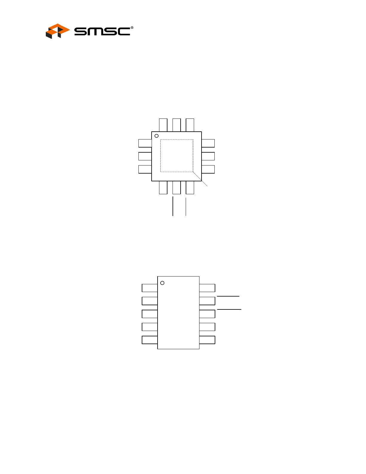
Chapter 1 Pin Description
Figure 1.1 EMC1701 Pin Diagram 12-Pin QFN 4mm x 4mm
Figure 1.2 EMC1701 Pin Diagram 10-Pin MSOP
2
3
4
5
6
9
8
7
VDD
SMCLK
SMDATA
1
12
11
10
AD
DR_SE
L
SENS
E
+
SENS
E
-
AL
E
R
T
T
H
_
SEL
THERM
DUR_SEL
N/C
N/C
GND
EMC
1701-1
EMC
1701-2
SMDATA
SMCLK
ALERT
VDD
THERM
GND
1
2
3
4
5
10
9
8
7
6
ADDR_SEL
SENSE+
SENSE-
N/C
High-Side Current-Sense and Internal 1°C Temperature Monitor
Datasheet
SMSC EMC1701
9
Revision 1.2 (09-27-10)
DATASHEET
The pin types are described in
Table 1.2
. All pins labeled with (5V) are 5V tolerant. All pins labeled
with (24V) are 24V tolerant.
Table 1.1 Pin Description for EMC1701
PIN
NUMBER
EMC1701-1
PIN
NUMBER
EMC1701-2
PIN NAME
PIN FUNCTION
PIN TYPE
1
5
VDD
Positive power supply voltage
Power (24V)
2
2
N/C
Not internally connected
n/a
3
N/A
N/C
Not internally connected
n/a
4
6
ADDR_SEL
Selects SMBus Address
AI
5
8
THERM
Active low output - requires pull-up resistor
OD (5V)
6
9
ALERT
Active low output - requires pull-up resistor
OD (5V)
7
10
SMDATA
SMBus data input/output - requires external
pull-up resistor
DIOD (5V)
8
1
SMCLK
SMBus clock input - requires external pull-
up resistor
DI (5V)
9
N/A
DUR_SEL
Selects peak detector duration
AI
10
N/A
TH_SEL
Selects peak detector threshold
AI
11
3
SENSE-
Negative current sense measurement point
AI (24V)
12
4
SENSE+
Positive current sense measurement point
AI (24V)
Bottom Pad
7
GND
Ground
Power
Table 1.2 Pin Types
PIN TYPE
DESCRIPTION
Power
This pin is used to supply power or ground to the device.
AI
Analog Input - this pin is used as an input for analog
signals.
OD
Open Drain Digital Output - this pin is used as a digital
output. It is open drain and requires a pull-up resistor.
This pin is 5V tolerant.
DI
Digital Input - this pin is used for digital inputs. This pin is
5V tolerant.
DIOD
Open Drain Digital Input / Output - this pin is bi-directional.
It is open drain and requires a pull-up resistor. This pin is
5V tolerant.
High-Side Current-Sense and Internal 1°C Temperature Monitor
Datasheet
Revision 1.2 (09-27-10)
10
SMSC EMC1701
DATASHEET
Chapter 2 Electrical Characteristics
Note 2.1
Stresses at or above those values listed could cause permanent damage to the device.
This is a stress rating only, and functional operation of the device at any other condition
above those indicated in the operation sections of this specification is not implied.
Prolonged stresses above the stated operating levels and below the Absolute Maximum
Ratings may degrade device performance and lead to permanent damage.
Note 2.2
All voltages are relative to ground.
Note 2.3
The Package Power Dissipation specification assumes a thermal via design with the
thermal landing be soldered to the PCB ground plane with four 12 mil vias (where
applicable).
Note 2.4
Junction to Ambient (
θ
JA
) is dependent on the design of the thermal vias. Without thermal
vias and a thermal landing, the
θ
JA
is approximately 60°C/W (EMC1701-1) including
localized PCB temperature increase.
Table 2.1 Absolute Maximum Ratings
Voltage on 5V tolerant pins
-0.3 to 5.5
V
Voltage on 2V tolerant pins
-0.3 to 2
V
Voltage on VDD, SENSE- and SENSE+ pins
-0.3 to 26
V
Voltage on any other pin to GND
-0.3 to 4
V
Voltage between Sense pins ( |(SENSE+ - SENSE-)| )
< 6
V
Package Power Dissipation
0.5W up to T
A
= 85°C
W
Junction to Ambient (
θ
JA
) (QFN12 package)
58
°C/W
Junction to Ambient (
θ
JA
) (MSOP10 package)
128
°C/W
Operating Ambient Temperature Range
-40 to 85
°C
Storage Temperature Range
-55 to 150
°C
ESD Rating - SMCLK, SMDATA, ALERT, THERM pins - HBM
4000
V
ESD Rating - All other pins - HBM
2000
V