

2014 Microchip Technology Inc.
DS20005273A-page
1
Data Sheet
PRODUCT FEATURES
EMC1412
Multiple Channel 1°C Temperature Sensor with
Beta Compensation
General Description
The EMC1412 is a high accuracy, low cost, System
Management Bus (SMBus) temperature sensor.
Advanced features such as Resistance Error Correction
(REC), Beta Compensation (to support CPU diodes
requiring the BJT/transistor model) and automatic diode
type detection combine to provide a robust solution for
complex environmental monitoring applications.
The EMC1412 monitors two temperature channels (one
external and one internal). It provides ±1°C accuracy for
both external and internal diode temperatures.
Resistance Error Correction automatically eliminates the
temperature error caused by series resistance allowing
greater flexibility in routing thermal diodes. Beta
Compensation eliminates temperature errors caused by
low, variable beta transistors common in today's fine
geometry processors. The automatic beta detection
feature monitors the external diode/transistor and
determines the optimum sensor settings for accurate
temperature measurements regardless of processor
technology. This frees the user from providing unique
sensor configurations for each temperature monitoring
application. These advanced features plus ±1°C
measurement accuracy provide a low-cost, highly
flexible and accurate solution for critical temperature
monitoring applications.
Applications
Notebook Computers
Desktop Computers
Industrial
Embedded applications
Features
Programmable SMBus address
Support for diodes requiring the BJT/transistor model
including advanced processor geometries
Automatically determines external diode type and
optimal settings
Resistance Error Correction
External Temperature Monitor
— ±1°C max accuracy (20°C < T
DIODE
< 110°C)
— 0.125°C resolution
— Supports up to 2.2nF diode filter capacitor
Internal Temperature Monitor
— ±1°C accuracy
— 0.125°C resolution
3.3V Supply Voltage
Programmable temperature limits for ALERT and
THERM
Available in small 8-pin 2mm x 3mm TDFN RoHS
compliant package
Available in small 8-pin MSOP RoHS compliant
package

REEL SIZE IS 4,000 PIECES FOR THE MSOP
REEL SIZE IS 5,000 PIECES FOR THE TDFN
This product meets the halogen maximum concentration values per IEC61249-2-21
ORDERING NUMBER
PACKAGE
FEATURES
SMBUS
ADDRESS
EMC1412-A-ACZL-TR
8-pin MSOP
(RoHS compliant
Two temperature sensors, ALERT and
THERM pins, programmable SMBus address
Selectable via
THERM pull-up
EMC1412-A-AC3-TR
8-pin TDFN 2mm x 3mm
(RoHS compliant
Two temperature sensors, ALERT and
THERM pins, fixed SMBus address
Selectable via
THERM pull-up
EMC1412-1-ACZL-TR
8-pin MSOP
(RoHS compliant
Two temperature sensors, ALERT and
THERM pins, fixed SMBus address
1001_100(r/w)
EMC1412-1-AC3-TR
8-pin TDFN 2mm x 3mm
(RoHS compliant
Two temperature sensors, ALERT and
THERM pins, fixed SMBus address
1001_100(r/w)
EMC1412-2-ACZL-TR
8-pin MSOP
(RoHS compliant
Two temperature sensors, ALERT and
THERM pins, fixed SMBus address
1001_101(r/w)
Multiple Channel 1°C Temperature Sensor with Beta Compensation
Data Sheet
DS20005273A-page
2
2014 Microchip Technology Inc.
TO OUR VALUED CUSTOMERS
It is our intention to provide our valued customers with the best documentation possible to ensure successful use of your Microchip
products. To this end, we will continue to improve our publications to better suit your needs. Our publications will be refined and
enhanced as new volumes and updates are introduced.
If you have any questions or comments regarding this publication, please contact the Marketing Communications Department via
E-mail at
docerrors@microchip.com
. We welcome your feedback.
Most Current Data Sheet
To obtain the most up-to-date version of this data sheet, please register at our Worldwide Web site at:
http://www.microchip.com
You can determine the version of a data sheet by examining its literature number found on the bottom outside corner of any page.
The last character of the literature number is the version number, (e.g., DS30000000A is version A of document DS30000000).
Errata
An errata sheet, describing minor operational differences from the data sheet and recommended workarounds, may exist for cur-
rent devices. As device/documentation issues become known to us, we will publish an errata sheet. The errata will specify the
revision of silicon and revision of document to which it applies.
To determine if an errata sheet exists for a particular device, please check with one of the following:
• Microchip’s Worldwide Web site;
http://www.microchip.com
• Your local Microchip sales office (see last page)
When contacting a sales office, please specify which device, revision of silicon and data sheet (include -literature number) you are
using.
Customer Notification System
Register on our web site at
www.microchip.com
to receive the most current information on all of our products.
Ordering Information:

Multiple Channel 1°C Temperature Sensor with Beta Compensation
Data Sheet
2014 Microchip Technology Inc.
DS20005273A-page
3
Table of Contents
Chapter
1
Block Diagram . . . . . . . . . . . . . . . . . . . . . . . . . . . . . . . . . . . . . . . . . . . . . . . . . . . . . 7
Chapter
2
Delta . . . . . . . . . . . . . . . . . . . . . . . . . . . . . . . . . . . . . . . . . . . . . . . . . . . . . . . . . . . . . 7
2.1
Functional Delta from EMC1412 rev A to rev B . . . . . . . . . . . . . . . . . . . . . . . . . . . . . . . . . . . . . . . . 7
Chapter
3
Pin Description . . . . . . . . . . . . . . . . . . . . . . . . . . . . . . . . . . . . . . . . . . . . . . . . . . . . . 8
Chapter
4
Electrical Specifications. . . . . . . . . . . . . . . . . . . . . . . . . . . . . . . . . . . . . . . . . . . . . 10
4.1
Absolute Maximum Ratings . . . . . . . . . . . . . . . . . . . . . . . . . . . . . . . . . . . . . . . . . . . . . . . . . . . . . . 10
4.2
Electrical Specifications . . . . . . . . . . . . . . . . . . . . . . . . . . . . . . . . . . . . . . . . . . . . . . . . . . . . . . . . . 11
4.3
SMBus Electrical Characteristics . . . . . . . . . . . . . . . . . . . . . . . . . . . . . . . . . . . . . . . . . . . . . . . . . . 12
Chapter
5
System Management Bus Interface Protocol . . . . . . . . . . . . . . . . . . . . . . . . . . . 13
5.1
Communications Protocol. . . . . . . . . . . . . . . . . . . . . . . . . . . . . . . . . . . . . . . . . . . . . . . . . . . . . . . . 13
5.1.1
SMBus Start Bit . . . . . . . . . . . . . . . . . . . . . . . . . . . . . . . . . . . . . . . . . . . . . . . . . . . . . . . . 13
5.1.2
SMBus Address and RD / WR Bit . . . . . . . . . . . . . . . . . . . . . . . . . . . . . . . . . . . . . . . . . . 13
5.1.3
THERM Pin Considerations. . . . . . . . . . . . . . . . . . . . . . . . . . . . . . . . . . . . . . . . . . . . . . . 14
5.1.4
SMBus Data Bytes. . . . . . . . . . . . . . . . . . . . . . . . . . . . . . . . . . . . . . . . . . . . . . . . . . . . . . 14
5.1.5
SMBus ACK and NACK Bits . . . . . . . . . . . . . . . . . . . . . . . . . . . . . . . . . . . . . . . . . . . . . . 14
5.1.6
SMBus Stop Bit . . . . . . . . . . . . . . . . . . . . . . . . . . . . . . . . . . . . . . . . . . . . . . . . . . . . . . . . 15
5.1.7
SMBus Timeout . . . . . . . . . . . . . . . . . . . . . . . . . . . . . . . . . . . . . . . . . . . . . . . . . . . . . . . . 15
5.1.8
SMBus and I
2
C Compatibility . . . . . . . . . . . . . . . . . . . . . . . . . . . . . . . . . . . . . . . . . . . . . 15
5.2
SMBus Protocols . . . . . . . . . . . . . . . . . . . . . . . . . . . . . . . . . . . . . . . . . . . . . . . . . . . . . . . . . . . . . . 15
5.2.1
Write Byte . . . . . . . . . . . . . . . . . . . . . . . . . . . . . . . . . . . . . . . . . . . . . . . . . . . . . . . . . . . . 15
5.2.2
Read Byte . . . . . . . . . . . . . . . . . . . . . . . . . . . . . . . . . . . . . . . . . . . . . . . . . . . . . . . . . . . . 16
5.2.3
Send Byte . . . . . . . . . . . . . . . . . . . . . . . . . . . . . . . . . . . . . . . . . . . . . . . . . . . . . . . . . . . . 16
5.2.4
Receive Byte . . . . . . . . . . . . . . . . . . . . . . . . . . . . . . . . . . . . . . . . . . . . . . . . . . . . . . . . . . 16
5.3
Alert Response Address . . . . . . . . . . . . . . . . . . . . . . . . . . . . . . . . . . . . . . . . . . . . . . . . . . . . . . . . . 16
Chapter
6
Product Description . . . . . . . . . . . . . . . . . . . . . . . . . . . . . . . . . . . . . . . . . . . . . . . . 18
6.1
Modes of Operation . . . . . . . . . . . . . . . . . . . . . . . . . . . . . . . . . . . . . . . . . . . . . . . . . . . . . . . . . . . . 18
6.1.1
Conversion Rates . . . . . . . . . . . . . . . . . . . . . . . . . . . . . . . . . . . . . . . . . . . . . . . . . . . . . . 18
6.1.2
Dynamic Averaging . . . . . . . . . . . . . . . . . . . . . . . . . . . . . . . . . . . . . . . . . . . . . . . . . . . . . 19
6.2
THERM Output . . . . . . . . . . . . . . . . . . . . . . . . . . . . . . . . . . . . . . . . . . . . . . . . . . . . . . . . . . . . . . . . 19
6.3
ALERT Output . . . . . . . . . . . . . . . . . . . . . . . . . . . . . . . . . . . . . . . . . . . . . . . . . . . . . . . . . . . . . . . . 20
6.3.1
ALERT Pin Interrupt Mode. . . . . . . . . . . . . . . . . . . . . . . . . . . . . . . . . . . . . . . . . . . . . . . . 20
6.3.2
ALERT Pin Comparator Mode . . . . . . . . . . . . . . . . . . . . . . . . . . . . . . . . . . . . . . . . . . . . . 20
6.4
Temperature Measurement . . . . . . . . . . . . . . . . . . . . . . . . . . . . . . . . . . . . . . . . . . . . . . . . . . . . . . 20
6.4.1
Beta Compensation . . . . . . . . . . . . . . . . . . . . . . . . . . . . . . . . . . . . . . . . . . . . . . . . . . . . . 20
6.4.2
Resistance Error Correction (REC) . . . . . . . . . . . . . . . . . . . . . . . . . . . . . . . . . . . . . . . . . 21
6.4.3
Programmable External Diode Ideality Factor . . . . . . . . . . . . . . . . . . . . . . . . . . . . . . . . . 21
6.5
Diode Faults . . . . . . . . . . . . . . . . . . . . . . . . . . . . . . . . . . . . . . . . . . . . . . . . . . . . . . . . . . . . . . . . . . 21
6.6
Consecutive Alerts . . . . . . . . . . . . . . . . . . . . . . . . . . . . . . . . . . . . . . . . . . . . . . . . . . . . . . . . . . . . . 21
6.7
Digital Filter. . . . . . . . . . . . . . . . . . . . . . . . . . . . . . . . . . . . . . . . . . . . . . . . . . . . . . . . . . . . . . . . . . . 21
6.8
Temperature Measurement Results and Data . . . . . . . . . . . . . . . . . . . . . . . . . . . . . . . . . . . . . . . . 23
6.9
External Diode Connections . . . . . . . . . . . . . . . . . . . . . . . . . . . . . . . . . . . . . . . . . . . . . . . . . . . . . . 24
Chapter
7
Register Description. . . . . . . . . . . . . . . . . . . . . . . . . . . . . . . . . . . . . . . . . . . . . . . . 25
7.1
Data Read Interlock . . . . . . . . . . . . . . . . . . . . . . . . . . . . . . . . . . . . . . . . . . . . . . . . . . . . . . . . . . . . 27
7.2
Temperature Data Registers . . . . . . . . . . . . . . . . . . . . . . . . . . . . . . . . . . . . . . . . . . . . . . . . . . . . . 27

Multiple Channel 1°C Temperature Sensor with Beta Compensation
Data Sheet
DS20005273A-page
4
2014 Microchip Technology Inc.
7.3
Status Register . . . . . . . . . . . . . . . . . . . . . . . . . . . . . . . . . . . . . . . . . . . . . . . . . . . . . . . . . . . . . . . . 27
7.4
Configuration Register . . . . . . . . . . . . . . . . . . . . . . . . . . . . . . . . . . . . . . . . . . . . . . . . . . . . . . . . . . 28
7.5
Conversion Rate Register. . . . . . . . . . . . . . . . . . . . . . . . . . . . . . . . . . . . . . . . . . . . . . . . . . . . . . . . 29
7.6
Limit Registers . . . . . . . . . . . . . . . . . . . . . . . . . . . . . . . . . . . . . . . . . . . . . . . . . . . . . . . . . . . . . . . . 30
7.7
Scratchpad Registers . . . . . . . . . . . . . . . . . . . . . . . . . . . . . . . . . . . . . . . . . . . . . . . . . . . . . . . . . . . 30
7.8
One Shot Register . . . . . . . . . . . . . . . . . . . . . . . . . . . . . . . . . . . . . . . . . . . . . . . . . . . . . . . . . . . . . 31
7.9
Therm Limit Registers. . . . . . . . . . . . . . . . . . . . . . . . . . . . . . . . . . . . . . . . . . . . . . . . . . . . . . . . . . . 31
7.10 Channel Mask Register . . . . . . . . . . . . . . . . . . . . . . . . . . . . . . . . . . . . . . . . . . . . . . . . . . . . . . . . . 31
7.11 Consecutive ALERT Register . . . . . . . . . . . . . . . . . . . . . . . . . . . . . . . . . . . . . . . . . . . . . . . . . . . . . 32
7.12 Beta Configuration Register . . . . . . . . . . . . . . . . . . . . . . . . . . . . . . . . . . . . . . . . . . . . . . . . . . . . . . 33
7.13 External Diode Ideality Factor Register . . . . . . . . . . . . . . . . . . . . . . . . . . . . . . . . . . . . . . . . . . . . . 34
7.14 Filter Control Register. . . . . . . . . . . . . . . . . . . . . . . . . . . . . . . . . . . . . . . . . . . . . . . . . . . . . . . . . . . 36
7.15 Product ID Register . . . . . . . . . . . . . . . . . . . . . . . . . . . . . . . . . . . . . . . . . . . . . . . . . . . . . . . . . . . . 36
7.16 Microchip ID Register . . . . . . . . . . . . . . . . . . . . . . . . . . . . . . . . . . . . . . . . . . . . . . . . . . . . . . . . . . . 36
7.17 Revision Register . . . . . . . . . . . . . . . . . . . . . . . . . . . . . . . . . . . . . . . . . . . . . . . . . . . . . . . . . . . . . . 37
Chapter
8
Typical Operating Curves. . . . . . . . . . . . . . . . . . . . . . . . . . . . . . . . . . . . . . . . . . . 38
Chapter
9
Package Information . . . . . . . . . . . . . . . . . . . . . . . . . . . . . . . . . . . . . . . . . . . . . . . 40
9.1
Package Markings . . . . . . . . . . . . . . . . . . . . . . . . . . . . . . . . . . . . . . . . . . . . . . . . . . . . . . . . . . . . . 42
Chapter
10 Data Sheet Revision History . . . . . . . . . . . . . . . . . . . . . . . . . . . . . . . . . . . . . . . . . 45

Multiple Channel 1°C Temperature Sensor with Beta Compensation
Data Sheet
2014 Microchip Technology Inc.
DS20005273A-page
5
List of Figures
Figure
1.1 EMC1412 Block Diagram. . . . . . . . . . . . . . . . . . . . . . . . . . . . . . . . . . . . . . . . . . . . . . . . . . . . . 7
Figure
3.1 EMC1412 Pin Diagram, MSOP-8. . . . . . . . . . . . . . . . . . . . . . . . . . . . . . . . . . . . . . . . . . . . . . . 8
Figure
3.2 EMC1412 Pin Diagram, TDFN-8 2mm x 3mm. . . . . . . . . . . . . . . . . . . . . . . . . . . . . . . . . . . . . 8
Figure
5.1 SMBus Timing Diagram . . . . . . . . . . . . . . . . . . . . . . . . . . . . . . . . . . . . . . . . . . . . . . . . . . . . . 13
Figure
5.2 Isolating
THERM Pin . . . . . . . . . . . . . . . . . . . . . . . . . . . . . . . . . . . . . . . . . . . . . . . . . . . . . . . 14
Figure
6.1 System Diagram for EMC1412 . . . . . . . . . . . . . . . . . . . . . . . . . . . . . . . . . . . . . . . . . . . . . . . 18
Figure
6.2 Temperature Filter Step Response . . . . . . . . . . . . . . . . . . . . . . . . . . . . . . . . . . . . . . . . . . . . 22
Figure
6.3 Temperature Filter Impulse Response. . . . . . . . . . . . . . . . . . . . . . . . . . . . . . . . . . . . . . . . . . 22
Figure
6.4 Diode Configurations . . . . . . . . . . . . . . . . . . . . . . . . . . . . . . . . . . . . . . . . . . . . . . . . . . . . . . . 24
Figure
9.1 EMC1412 2mm x 3mm TDFN Package Drawing. . . . . . . . . . . . . . . . . . . . . . . . . . . . . . . . . . 40
Figure
9.2 8-Pin MSOP / TSSOP Package . . . . . . . . . . . . . . . . . . . . . . . . . . . . . . . . . . . . . . . . . . . . . . . 41
Figure
9.3 EMC1412-1 8-Pin TDFN Package Markings . . . . . . . . . . . . . . . . . . . . . . . . . . . . . . . . . . . . . 42
Figure
9.4 EMC1412-A 8-Pin TDFN Package Markings . . . . . . . . . . . . . . . . . . . . . . . . . . . . . . . . . . . . . 43
Figure
9.5 EMC1412 8-Pin MSOP Package Markings . . . . . . . . . . . . . . . . . . . . . . . . . . . . . . . . . . . . . . 44

Multiple Channel 1°C Temperature Sensor with Beta Compensation
Data Sheet
DS20005273A-page
6
2014 Microchip Technology Inc.
List of Tables
Table
3.1 EMC1412 Pin Description . . . . . . . . . . . . . . . . . . . . . . . . . . . . . . . . . . . . . . . . . . . . . . . . . . . . . 8
Table
3.2 Pin Types. . . . . . . . . . . . . . . . . . . . . . . . . . . . . . . . . . . . . . . . . . . . . . . . . . . . . . . . . . . . . . . . . . 9
Table
4.1 Absolute Maximum Ratings . . . . . . . . . . . . . . . . . . . . . . . . . . . . . . . . . . . . . . . . . . . . . . . . . . . 10
Table
4.2 Electrical Specifications . . . . . . . . . . . . . . . . . . . . . . . . . . . . . . . . . . . . . . . . . . . . . . . . . . . . . . 11
Table
4.3 SMBus Electrical Specifications . . . . . . . . . . . . . . . . . . . . . . . . . . . . . . . . . . . . . . . . . . . . . . . 12
Table
5.1 SMBus Address Decode . . . . . . . . . . . . . . . . . . . . . . . . . . . . . . . . . . . . . . . . . . . . . . . . . . . . . 13
Table
5.2 Protocol Format . . . . . . . . . . . . . . . . . . . . . . . . . . . . . . . . . . . . . . . . . . . . . . . . . . . . . . . . . . . . 15
Table
5.3 Write Byte Protocol . . . . . . . . . . . . . . . . . . . . . . . . . . . . . . . . . . . . . . . . . . . . . . . . . . . . . . . . . 15
Table
5.4 Read Byte Protocol . . . . . . . . . . . . . . . . . . . . . . . . . . . . . . . . . . . . . . . . . . . . . . . . . . . . . . . . . 16
Table
5.5 Send Byte Protocol . . . . . . . . . . . . . . . . . . . . . . . . . . . . . . . . . . . . . . . . . . . . . . . . . . . . . . . . . 16
Table
5.6 Receive Byte Protocol . . . . . . . . . . . . . . . . . . . . . . . . . . . . . . . . . . . . . . . . . . . . . . . . . . . . . . . 16
Table
5.7 Alert Response Address Protocol . . . . . . . . . . . . . . . . . . . . . . . . . . . . . . . . . . . . . . . . . . . . . . 16
Table
6.1 Supply Current vs. Conversion Rate for EMC1412 . . . . . . . . . . . . . . . . . . . . . . . . . . . . . . . . . 19
Table
6.2 Temperature Data Format . . . . . . . . . . . . . . . . . . . . . . . . . . . . . . . . . . . . . . . . . . . . . . . . . . . . 23
Table
7.1 Register Set in Hexadecimal Order . . . . . . . . . . . . . . . . . . . . . . . . . . . . . . . . . . . . . . . . . . . . . 25
Table
7.2 Temperature Data Registers . . . . . . . . . . . . . . . . . . . . . . . . . . . . . . . . . . . . . . . . . . . . . . . . . . 27
Table
7.3 Status Register . . . . . . . . . . . . . . . . . . . . . . . . . . . . . . . . . . . . . . . . . . . . . . . . . . . . . . . . . . . . 27
Table
7.4 Configuration Register . . . . . . . . . . . . . . . . . . . . . . . . . . . . . . . . . . . . . . . . . . . . . . . . . . . . . . . 28
Table
7.5 Conversion Rate Register . . . . . . . . . . . . . . . . . . . . . . . . . . . . . . . . . . . . . . . . . . . . . . . . . . . . 29
Table
7.6 Conversion Rate . . . . . . . . . . . . . . . . . . . . . . . . . . . . . . . . . . . . . . . . . . . . . . . . . . . . . . . . . . . 29
Table
7.7 Temperature Limit Registers . . . . . . . . . . . . . . . . . . . . . . . . . . . . . . . . . . . . . . . . . . . . . . . . . . 30
Table
7.8 Scratchpad Register . . . . . . . . . . . . . . . . . . . . . . . . . . . . . . . . . . . . . . . . . . . . . . . . . . . . . . . . 30
Table
7.9 One Shot Register . . . . . . . . . . . . . . . . . . . . . . . . . . . . . . . . . . . . . . . . . . . . . . . . . . . . . . . . . . 31
Table
7.10 Therm Limit Registers . . . . . . . . . . . . . . . . . . . . . . . . . . . . . . . . . . . . . . . . . . . . . . . . . . . . . . . 31
Table
7.11 Channel Mask Register . . . . . . . . . . . . . . . . . . . . . . . . . . . . . . . . . . . . . . . . . . . . . . . . . . . . . . 31
Table
7.12 Consecutive ALERT Register . . . . . . . . . . . . . . . . . . . . . . . . . . . . . . . . . . . . . . . . . . . . . . . . . 32
Table
7.13 Consecutive Alert / Therm Settings . . . . . . . . . . . . . . . . . . . . . . . . . . . . . . . . . . . . . . . . . . . . . 33
Table
7.14 Beta Configuration Register. . . . . . . . . . . . . . . . . . . . . . . . . . . . . . . . . . . . . . . . . . . . . . . . . . . 33
Table
7.15 CPU Beta Values. . . . . . . . . . . . . . . . . . . . . . . . . . . . . . . . . . . . . . . . . . . . . . . . . . . . . . . . . . . 34
Table
7.16 Ideality Configuration Registers. . . . . . . . . . . . . . . . . . . . . . . . . . . . . . . . . . . . . . . . . . . . . . . . 34
Table
7.17 Ideality Factor Look-Up Table (Diode Model) . . . . . . . . . . . . . . . . . . . . . . . . . . . . . . . . . . . . . 34
Table
7.18 Substrate Diode Ideality Factor Look-Up Table (BJT Model) . . . . . . . . . . . . . . . . . . . . . . . . . 35
Table
7.19 Filter Configuration Register . . . . . . . . . . . . . . . . . . . . . . . . . . . . . . . . . . . . . . . . . . . . . . . . . . 36
Table
7.20 FILTER Decode . . . . . . . . . . . . . . . . . . . . . . . . . . . . . . . . . . . . . . . . . . . . . . . . . . . . . . . . . . . . 36
Table
7.21 Product ID Register . . . . . . . . . . . . . . . . . . . . . . . . . . . . . . . . . . . . . . . . . . . . . . . . . . . . . . . . . 36
Table
7.22 Manufacturer ID Register. . . . . . . . . . . . . . . . . . . . . . . . . . . . . . . . . . . . . . . . . . . . . . . . . . . . . 36
Table
7.23 Revision Register. . . . . . . . . . . . . . . . . . . . . . . . . . . . . . . . . . . . . . . . . . . . . . . . . . . . . . . . . . . 37
Table
10.1 Revision History. . . . . . . . . . . . . . . . . . . . . . . . . . . . . . . . . . . . . . . . . . . . . . . . . . . . . . . . . . . . 45
Multiple Channel 1°C Temperature Sensor with Beta Compensation
Data Sheet
2014 Microchip Technology Inc.
DS20005273A-page
7
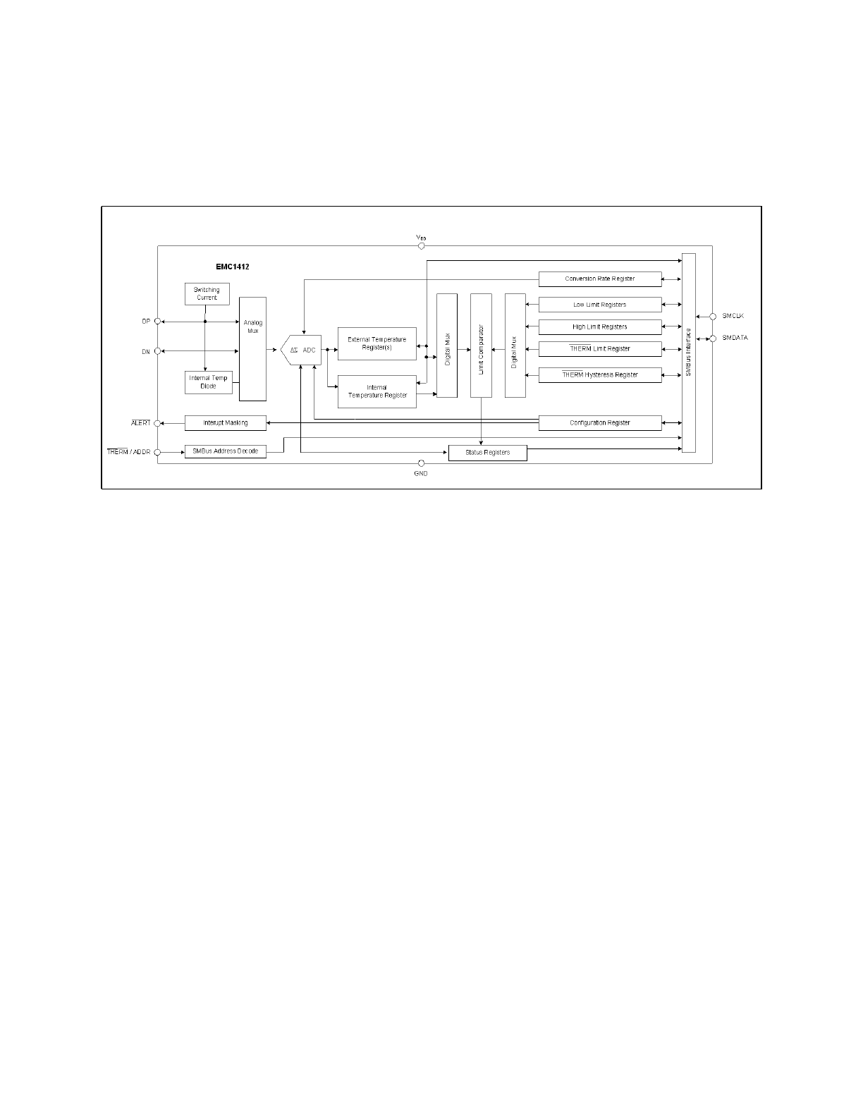
Chapter
1
Block
Diagram
Figure
1.1
EMC1412
Block
Diagram
Chapter
2
Delta
2.1
Functional Delta from EMC1412 rev A to rev B
1. Updated revision number to 04h.
Multiple Channel 1°C Temperature Sensor with Beta Compensation
Data Sheet
DS20005273A-page
8
2014 Microchip Technology Inc.
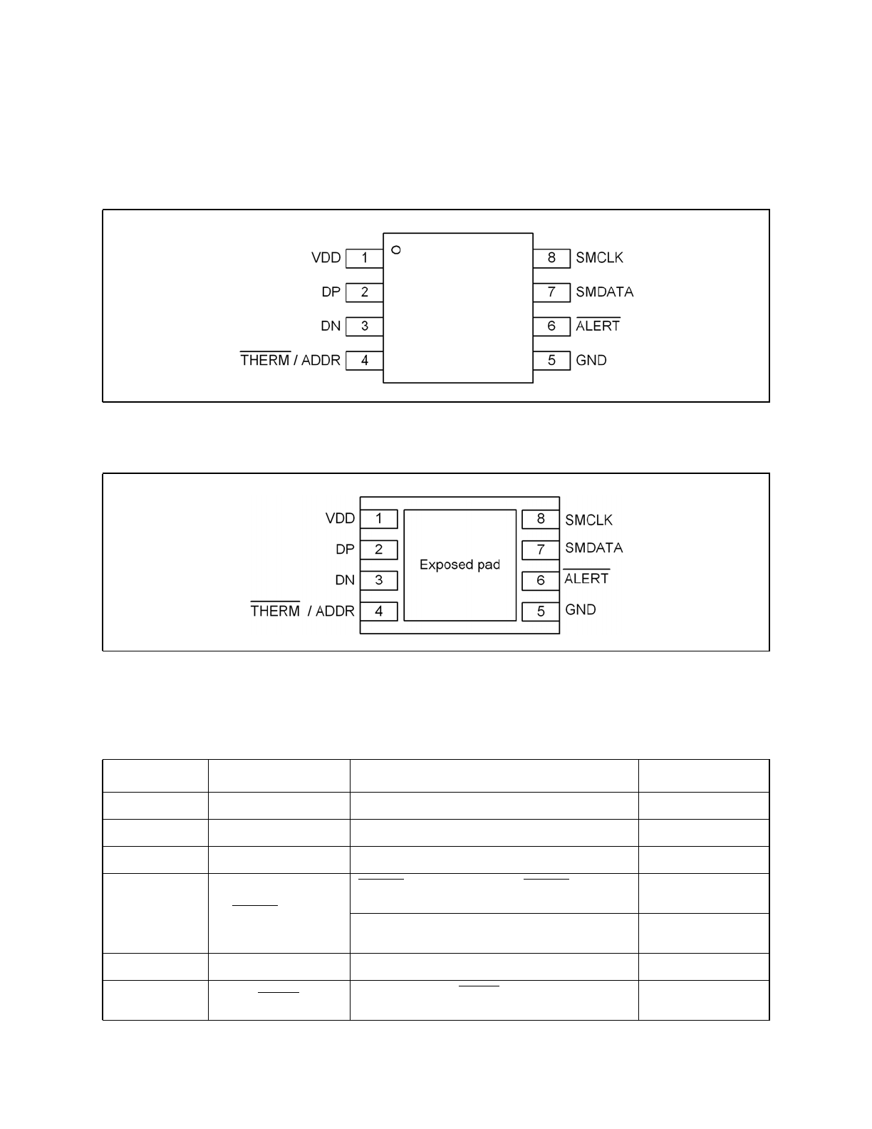
Chapter
3
Pin
Description
Figure
3.1
EMC1412
Pin
Diagram,
MSOP-8
Figure
3.2 EMC1412 Pin Diagram, TDFN-8 2mm x 3mm
Table
3.1 EMC1412 Pin Description
PIN NUMBER
NAME
FUNCTION
TYPE
1
VDD
Power supply
Power
2
DP
External diode positive (anode) connection
AIO
3
DN
External diode negative (cathode) connection
AIO
4
THERM / ADDR
THERM - Active low Critical THERM output
signal - requires pull-up resistor
OD (5V)
ADDR - Selects SMBus address based on pull-
up resistor
OD (5V)
5
GND
Ground
Power
6
ALERT
Active low digital ALERT output signal -
requires pull-up resistor
OD (5V)
Multiple Channel 1°C Temperature Sensor with Beta Compensation
Data Sheet
2014 Microchip Technology Inc.
DS20005273A-page
9
APPLICATION NOTE:
For the 5V tolerant pins that have a pull-up resistor (SMCLK, SMDATA, THERM, and
ALERT), the voltage difference between VDD and the pull-up voltage must never exceed
3.6V.
The pin types are described
Table
3.2
.
7
SMDATA
SMBus Data input/output - requires pull-up
resistor
DIOD (5V)
8
SMCLK
SMBus Clock input - requires pull-up resistor
DI (5V)
Bottom Pad
Exposed Pad
Not internally connected, but recommend
grounding.
-
Table
3.2 Pin Types
PIN TYPE
DESCRIPTION
Power
This pin is used to supply power or ground to the device.
AIO
Analog Input / Output -This pin is used as an I/O for analog signals.
DI
Digital Input - This pin is used as a digital input. This pin is 5V tolerant.
DIOD
Digital Input / Open Drain Output - This pin is used as a digital I/O. When it is used as
an output, it is open drain and requires a pull-up resistor. This pin is 5V tolerant.
OD
Open Drain Digital Output - This pin is used as a digital output. It is open drain and
requires a pull-up resistor. This pin is 5V tolerant.
Table
3.1 EMC1412 Pin Description (continued)
PIN NUMBER
NAME
FUNCTION
TYPE

Multiple Channel 1°C Temperature Sensor with Beta Compensation
Data Sheet
DS20005273A-page
10
2014 Microchip Technology Inc.
Chapter
4 Electrical Specifications
4.1
Absolute Maximum Ratings
Note:
Stresses at or above those listed could cause permanent damage to the device. This is a stress
rating only and functional operation of the device at any other condition above those indicated
in the operation sections of this specification is not implied.
Note
4.1
For the 5V tolerant pins that have a pull-up resistor (SMCLK, SMDATA, THERM, and
ALERT), the pull-up voltage must not exceed 3.6V when the device is unpowered.
Table
4.1 Absolute Maximum Ratings
DESCRIPTION
RATING
UNIT
Supply Voltage (V
DD
)
-0.3 to 4.0
V
Voltage on 5V tolerant pins (V
5VT_pin
)
-0.3 to 5.5
V
Voltage on 5V tolerant pins (|V
5VT_pin
- V
DD
|) (see
Note
4.1
)
0 to 3.6
V
Voltage on any other pin to Ground
-0.3 to V
DD
+0.3
V
Operating Temperature Range
-40 to +125
°C
Storage Temperature Range
-55 to +150
°C
Lead Temperature Range
Refer to JEDEC Spec. J-STD-020
Package Thermal Characteristics for MSOP-8
Thermal Resistance (
j-a
)
140.8
°C/W
Package Thermal Characteristics for TDFN-8
Thermal Resistance (
j-a
)
89
°C/W
ESD Rating, All pins HBM
2000
V