
SMSC EMC1073 / EMC1074
DATASHEET
Revision 1.39 (10-11-10)
Datasheet
PRODUCT FEATURES
EMC1073 / EMC1074
Multiple Channel 1°C
Temperature Sensors with
Selectable Address
General Description
The EMC1073 and EMC1074 are high accuracy, low
cost, System Management Bus (SMBus) temperature
sensors with pin selectable SMBus addresses.
Each device provides ±1° accuracy (max) for external
diode temperatures and ±2°C accuracy (max) for the
internal diode temperature. The EMC1073 monitors
three temperature channels (two external and one
internal). The EMC1074 monitors four temperature
channels (three external and one internal).
Applications
Notebook Computers
Desktop Computers
Industrial
Embedded applications
Features
External Temperature Monitors
—
±0.25°C typ accuracy (20°C < T
DIODE
< 110°C)
—
0.125°C resolution
—
Supports 2N3904 and AMD diodes
—
Anti-parallel diodes for extra diode support (EMC1074)
Internal Temperature Monitor
—
±0.25°C typ accuracy (-5°C < T
A
< 100°C)
3.3V Supply Voltage
SMBus 2.0 Compliant
—
Programmable SMBus address
Programmable Temperature Limits for ALERT and
THERM
Available in Small 10-pin MSOP Lead-free RoHS
Compliant Package
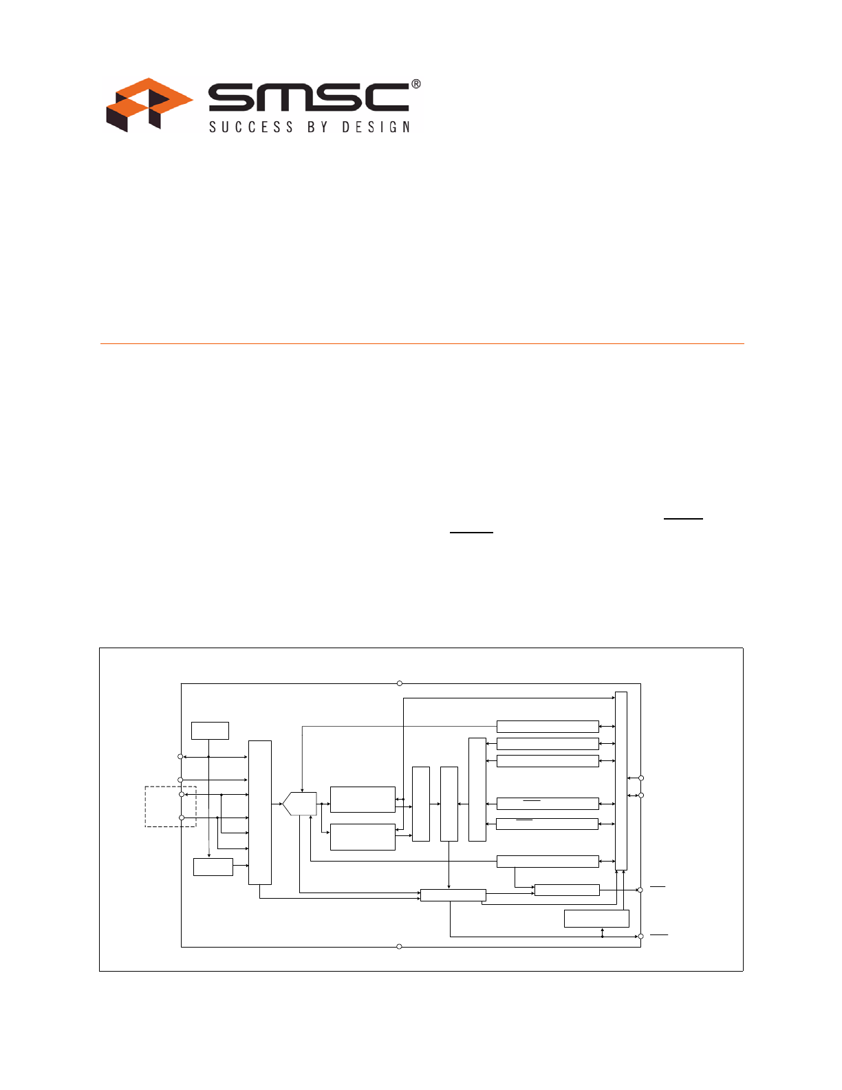
Block Diagram
Internal Temp
Diode
Switching
Current
Analog
Mux
Internal
Temperature Register
Dig
it
a
l Mu
x
Dig
it
a
l Mu
x
L
imit
Co
m
p
ar
at
o
r
Low Limit Registers
High Limit Registers
Conversion Rate Register
Interupt Masking
Status Registers
Configuration Register
SM
B
u
s
In
te
rf
ac
e
ALERT
THERM/ADDR
SMCLK
SMDATA
DP1
DN1
VDD
GND
EMC1073 / EMC1074
External Temperature
Register(s)
ΔΣ ADC
THERM Limit Register
THERM Hysteresis Register
SMBus Address Decode
Anti-parallel
Diode
DP2 / DN3
*
DN2 / DP3
*
* DN3 and DP3 are EMC1074 only

Order Number(s):
EMC1073-1-AIZL-TR for 10-pin, MSOP Lead-Free RoHS Compliant Package
EMC1073-A-AIZL-TR for 10-pin, MSOP Lead-Free RoHS Compliant Package
EMC1074-1-AIZL-TR for 10-pin, MSOP Lead-Free RoHS Compliant Package
EMC1074-A-AIZL-TR for 10-pin, MSOP Lead-Free RoHS Compliant Package
Note: See
Table 1.1, "Part Selection"
for SMBus addressing options.
Reel size is 4,000 pieces
This product meets the halogen maximum concentration values per IEC61249-2-21
For RoHS compliance and environmental information, please visit
www.smsc.com/rohs
Multiple Channel 1°C Temperature Sensors with Selectable Address
Datasheet
Revision 1.39 (10-11-10)
2
SMSC EMC1073 / EMC1074
DATASHEET
80 ARKAY DRIVE, HAUPPAUGE, NY 11788 (631) 435-6000, FAX (631) 273-3123
Copyright © 2010 SMSC or its subsidiaries. All rights reserved.
Circuit diagrams and other information relating to SMSC products are included as a means of illustrating typical applications. Consequently, complete information sufficient for
construction purposes is not necessarily given. Although the information has been checked and is believed to be accurate, no responsibility is assumed for inaccuracies. SMSC
reserves the right to make changes to specifications and product descriptions at any time without notice. Contact your local SMSC sales office to obtain the latest specifications
before placing your product order. The provision of this information does not convey to the purchaser of the described semiconductor devices any licenses under any patent
rights or other intellectual property rights of SMSC or others. All sales are expressly conditional on your agreement to the terms and conditions of the most recently dated
version of SMSC's standard Terms of Sale Agreement dated before the date of your order (the "Terms of Sale Agreement"). The product may contain design defects or errors
known as anomalies which may cause the product's functions to deviate from published specifications. Anomaly sheets are available upon request. SMSC products are not
designed, intended, authorized or warranted for use in any life support or other application where product failure could cause or contribute to personal injury or severe property
damage. Any and all such uses without prior written approval of an Officer of SMSC and further testing and/or modification will be fully at the risk of the customer. Copies of
this document or other SMSC literature, as well as the Terms of Sale Agreement, may be obtained by visiting SMSC’s website at http://www.smsc.com. SMSC is a registered
trademark of Standard Microsystems Corporation (“SMSC”). Product names and company names are the trademarks of their respective holders.
SMSC DISCLAIMS AND EXCLUDES ANY AND ALL WARRANTIES, INCLUDING WITHOUT LIMITATION ANY AND ALL IMPLIED WARRANTIES OF MERCHANTABILITY,
FITNESS FOR A PARTICULAR PURPOSE, TITLE, AND AGAINST INFRINGEMENT AND THE LIKE, AND ANY AND ALL WARRANTIES ARISING FROM ANY COURSE
OF DEALING OR USAGE OF TRADE. IN NO EVENT SHALL SMSC BE LIABLE FOR ANY DIRECT, INCIDENTAL, INDIRECT, SPECIAL, PUNITIVE, OR CONSEQUENTIAL
DAMAGES; OR FOR LOST DATA, PROFITS, SAVINGS OR REVENUES OF ANY KIND; REGARDLESS OF THE FORM OF ACTION, WHETHER BASED ON CONTRACT;
TORT; NEGLIGENCE OF SMSC OR OTHERS; STRICT LIABILITY; BREACH OF WARRANTY; OR OTHERWISE; WHETHER OR NOT ANY REMEDY OF BUYER IS HELD
TO HAVE FAILED OF ITS ESSENTIAL PURPOSE, AND WHETHER OR NOT SMSC HAS BEEN ADVISED OF THE POSSIBILITY OF SUCH DAMAGES.

Multiple Channel 1°C Temperature Sensors with Selectable Address
Datasheet
SMSC EMC1073 / EMC1074
3
Revision 1.39 (10-11-10)
DATASHEET
Table of Contents
Chapter 1
Part Selection . . . . . . . . . . . . . . . . . . . . . . . . . . . . . . . . . . . . . . . . . . . . . . . . . . . . . . 7
Chapter 2
Pin Description . . . . . . . . . . . . . . . . . . . . . . . . . . . . . . . . . . . . . . . . . . . . . . . . . . . . . 8
Chapter 3
Electrical Specifications . . . . . . . . . . . . . . . . . . . . . . . . . . . . . . . . . . . . . . . . . . . . 10
3.1
Absolute Maximum Ratings . . . . . . . . . . . . . . . . . . . . . . . . . . . . . . . . . . . . . . . . . . . . . . . . . . . . . . 10
3.2
Electrical Specifications . . . . . . . . . . . . . . . . . . . . . . . . . . . . . . . . . . . . . . . . . . . . . . . . . . . . . . . . . 11
3.3
SMBus Electrical Characteristics . . . . . . . . . . . . . . . . . . . . . . . . . . . . . . . . . . . . . . . . . . . . . . . . . . 12
Chapter 4
System Management Bus Interface Protocol . . . . . . . . . . . . . . . . . . . . . . . . . . . 13
4.1
System Management Bus Interface Protocol . . . . . . . . . . . . . . . . . . . . . . . . . . . . . . . . . . . . . . . . . 13
4.2
Write Byte . . . . . . . . . . . . . . . . . . . . . . . . . . . . . . . . . . . . . . . . . . . . . . . . . . . . . . . . . . . . . . . . . . . . 13
4.3
Read Byte . . . . . . . . . . . . . . . . . . . . . . . . . . . . . . . . . . . . . . . . . . . . . . . . . . . . . . . . . . . . . . . . . . . . 14
4.4
Send Byte . . . . . . . . . . . . . . . . . . . . . . . . . . . . . . . . . . . . . . . . . . . . . . . . . . . . . . . . . . . . . . . . . . . . 14
4.5
Receive Byte. . . . . . . . . . . . . . . . . . . . . . . . . . . . . . . . . . . . . . . . . . . . . . . . . . . . . . . . . . . . . . . . . . 14
4.6
Alert Response Address . . . . . . . . . . . . . . . . . . . . . . . . . . . . . . . . . . . . . . . . . . . . . . . . . . . . . . . . . 14
4.7
SMBus Address . . . . . . . . . . . . . . . . . . . . . . . . . . . . . . . . . . . . . . . . . . . . . . . . . . . . . . . . . . . . . . . 15
4.8
SMBus Timeout . . . . . . . . . . . . . . . . . . . . . . . . . . . . . . . . . . . . . . . . . . . . . . . . . . . . . . . . . . . . . . . 15
Chapter 5
Product Description . . . . . . . . . . . . . . . . . . . . . . . . . . . . . . . . . . . . . . . . . . . . . . . . 16
5.1
Modes of Operation . . . . . . . . . . . . . . . . . . . . . . . . . . . . . . . . . . . . . . . . . . . . . . . . . . . . . . . . . . . . 17
5.1.1
Conversion Rates . . . . . . . . . . . . . . . . . . . . . . . . . . . . . . . . . . . . . . . . . . . . . . . . . . . . . . 17
5.1.2
Dynamic Averaging . . . . . . . . . . . . . . . . . . . . . . . . . . . . . . . . . . . . . . . . . . . . . . . . . . . . . 17
5.2
THERM Output . . . . . . . . . . . . . . . . . . . . . . . . . . . . . . . . . . . . . . . . . . . . . . . . . . . . . . . . . . . . . . . . 18
5.2.1
THERM Pin Considerations. . . . . . . . . . . . . . . . . . . . . . . . . . . . . . . . . . . . . . . . . . . . . . . 19
5.3
ALERT Output . . . . . . . . . . . . . . . . . . . . . . . . . . . . . . . . . . . . . . . . . . . . . . . . . . . . . . . . . . . . . . . . 19
5.3.1
ALERT Pin Interrupt Mode . . . . . . . . . . . . . . . . . . . . . . . . . . . . . . . . . . . . . . . . . . . . . . . 19
5.3.2
ALERT Pin Comparator Mode . . . . . . . . . . . . . . . . . . . . . . . . . . . . . . . . . . . . . . . . . . . . . 19
5.4
Programmable External Diode Ideality Factor . . . . . . . . . . . . . . . . . . . . . . . . . . . . . . . . . . . . . . . . 20
5.5
Diode Faults . . . . . . . . . . . . . . . . . . . . . . . . . . . . . . . . . . . . . . . . . . . . . . . . . . . . . . . . . . . . . . . . . . 20
5.6
Consecutive Alerts . . . . . . . . . . . . . . . . . . . . . . . . . . . . . . . . . . . . . . . . . . . . . . . . . . . . . . . . . . . . . 20
5.7
Digital Filter. . . . . . . . . . . . . . . . . . . . . . . . . . . . . . . . . . . . . . . . . . . . . . . . . . . . . . . . . . . . . . . . . . . 20
5.8
Temperature Monitors . . . . . . . . . . . . . . . . . . . . . . . . . . . . . . . . . . . . . . . . . . . . . . . . . . . . . . . . . . 22
5.9
Temperature Measurement Results and Data . . . . . . . . . . . . . . . . . . . . . . . . . . . . . . . . . . . . . . . . 22
5.10
Anti-parallel Diode Connections . . . . . . . . . . . . . . . . . . . . . . . . . . . . . . . . . . . . . . . . . . . . . . . . . . . 23
5.11
External Diode Connections . . . . . . . . . . . . . . . . . . . . . . . . . . . . . . . . . . . . . . . . . . . . . . . . . . . . . . 23
Chapter 6
Register Description . . . . . . . . . . . . . . . . . . . . . . . . . . . . . . . . . . . . . . . . . . . . . . . 25
6.1
Data Read Interlock . . . . . . . . . . . . . . . . . . . . . . . . . . . . . . . . . . . . . . . . . . . . . . . . . . . . . . . . . . . . 28
6.2
Temperature Data Registers . . . . . . . . . . . . . . . . . . . . . . . . . . . . . . . . . . . . . . . . . . . . . . . . . . . . . 28
6.3
Status Register . . . . . . . . . . . . . . . . . . . . . . . . . . . . . . . . . . . . . . . . . . . . . . . . . . . . . . . . . . . . . . . . 29
6.4
Configuration Register . . . . . . . . . . . . . . . . . . . . . . . . . . . . . . . . . . . . . . . . . . . . . . . . . . . . . . . . . . 29
6.5
Conversion Rate Register. . . . . . . . . . . . . . . . . . . . . . . . . . . . . . . . . . . . . . . . . . . . . . . . . . . . . . . . 30
6.6
Limit Registers . . . . . . . . . . . . . . . . . . . . . . . . . . . . . . . . . . . . . . . . . . . . . . . . . . . . . . . . . . . . . . . . 31
6.7
Scratchpad Registers . . . . . . . . . . . . . . . . . . . . . . . . . . . . . . . . . . . . . . . . . . . . . . . . . . . . . . . . . . . 32
6.8
One Shot Register . . . . . . . . . . . . . . . . . . . . . . . . . . . . . . . . . . . . . . . . . . . . . . . . . . . . . . . . . . . . . 33
6.9
Therm Limit Registers. . . . . . . . . . . . . . . . . . . . . . . . . . . . . . . . . . . . . . . . . . . . . . . . . . . . . . . . . . . 33
6.10
External Diode Fault Register. . . . . . . . . . . . . . . . . . . . . . . . . . . . . . . . . . . . . . . . . . . . . . . . . . . . . 33
6.11
Channel Mask Register . . . . . . . . . . . . . . . . . . . . . . . . . . . . . . . . . . . . . . . . . . . . . . . . . . . . . . . . . 34
6.12
Consecutive ALERT Register . . . . . . . . . . . . . . . . . . . . . . . . . . . . . . . . . . . . . . . . . . . . . . . . . . . . . 34
6.13
External Diode Ideality Factor Registers . . . . . . . . . . . . . . . . . . . . . . . . . . . . . . . . . . . . . . . . . . . . 36

Multiple Channel 1°C Temperature Sensors with Selectable Address
Datasheet
Revision 1.39 (10-11-10)
4
SMSC EMC1073 / EMC1074
DATASHEET
6.14
High Limit Status Register . . . . . . . . . . . . . . . . . . . . . . . . . . . . . . . . . . . . . . . . . . . . . . . . . . . . . . . 37
6.15
Low Limit Status Register . . . . . . . . . . . . . . . . . . . . . . . . . . . . . . . . . . . . . . . . . . . . . . . . . . . . . . . . 37
6.16
THERM Limit Status Register. . . . . . . . . . . . . . . . . . . . . . . . . . . . . . . . . . . . . . . . . . . . . . . . . . . . . 38
6.17
Filter Control Register. . . . . . . . . . . . . . . . . . . . . . . . . . . . . . . . . . . . . . . . . . . . . . . . . . . . . . . . . . . 38
6.18
Product ID Register . . . . . . . . . . . . . . . . . . . . . . . . . . . . . . . . . . . . . . . . . . . . . . . . . . . . . . . . . . . . 39
6.19
SMSC ID Register (FEh) . . . . . . . . . . . . . . . . . . . . . . . . . . . . . . . . . . . . . . . . . . . . . . . . . . . . . . . . 39
6.20
Revision Register (FFh) . . . . . . . . . . . . . . . . . . . . . . . . . . . . . . . . . . . . . . . . . . . . . . . . . . . . . . . . . 39
Chapter 7
Typical Operating Curves. . . . . . . . . . . . . . . . . . . . . . . . . . . . . . . . . . . . . . . . . . . 40
Chapter 8
Package Information . . . . . . . . . . . . . . . . . . . . . . . . . . . . . . . . . . . . . . . . . . . . . . . 42
8.1
Package Markings . . . . . . . . . . . . . . . . . . . . . . . . . . . . . . . . . . . . . . . . . . . . . . . . . . . . . . . . . . . . . 43
Chapter 9
Datasheet Revision History . . . . . . . . . . . . . . . . . . . . . . . . . . . . . . . . . . . . . . . . . . 45

Multiple Channel 1°C Temperature Sensors with Selectable Address
Datasheet
SMSC EMC1073 / EMC1074
5
Revision 1.39 (10-11-10)
DATASHEET
List of Figures
Figure 2.1 EMC1073/EMC1074 Pin Diagram, MSOP-10 . . . . . . . . . . . . . . . . . . . . . . . . . . . . . . . . . . . . . 8
Figure 4.1 SMBus Timing Diagram . . . . . . . . . . . . . . . . . . . . . . . . . . . . . . . . . . . . . . . . . . . . . . . . . . . . . 13
Figure 5.1 System Diagram for EMC1073 . . . . . . . . . . . . . . . . . . . . . . . . . . . . . . . . . . . . . . . . . . . . . . . 16
Figure 5.2 System Diagram for EMC1074 . . . . . . . . . . . . . . . . . . . . . . . . . . . . . . . . . . . . . . . . . . . . . . . 16
Figure 5.3 Isolating THERM Pin . . . . . . . . . . . . . . . . . . . . . . . . . . . . . . . . . . . . . . . . . . . . . . . . . . . . . . . 19
Figure 5.4 Temperature Filter Step Response . . . . . . . . . . . . . . . . . . . . . . . . . . . . . . . . . . . . . . . . . . . . 21
Figure 5.5 Temperature Filter Impulse Response. . . . . . . . . . . . . . . . . . . . . . . . . . . . . . . . . . . . . . . . . . 21
Figure 5.6 EMC1073 Diode Configurations. . . . . . . . . . . . . . . . . . . . . . . . . . . . . . . . . . . . . . . . . . . . . . . 24
Figure 5.7 EMC1074 Diode Configurations. . . . . . . . . . . . . . . . . . . . . . . . . . . . . . . . . . . . . . . . . . . . . . . 24
Figure 8.1 10-Pin MSOP / TSSOP Package . . . . . . . . . . . . . . . . . . . . . . . . . . . . . . . . . . . . . . . . . . . . . . 42
Figure 8.2 EMC1073 Package Markings - 10-Pin MSOP . . . . . . . . . . . . . . . . . . . . . . . . . . . . . . . . . . . . 43
Figure 8.3 EMC1074 Package Markings - 10-Pin MSOP . . . . . . . . . . . . . . . . . . . . . . . . . . . . . . . . . . . . 44

Multiple Channel 1°C Temperature Sensors with Selectable Address
Datasheet
Revision 1.39 (10-11-10)
6
SMSC EMC1073 / EMC1074
DATASHEET
List of Tables
Table 1.1 Part Selection . . . . . . . . . . . . . . . . . . . . . . . . . . . . . . . . . . . . . . . . . . . . . . . . . . . . . . . . . . . . . . 7
Table 2.1 EMC1073 and EMC1074 Pin Description . . . . . . . . . . . . . . . . . . . . . . . . . . . . . . . . . . . . . . . . . 8
Table 3.1 Absolute Maximum Ratings . . . . . . . . . . . . . . . . . . . . . . . . . . . . . . . . . . . . . . . . . . . . . . . . . . . 10
Table 3.2 Electrical Specifications . . . . . . . . . . . . . . . . . . . . . . . . . . . . . . . . . . . . . . . . . . . . . . . . . . . . . . 11
Table 3.3 SMBus Electrical Specifications . . . . . . . . . . . . . . . . . . . . . . . . . . . . . . . . . . . . . . . . . . . . . . . 12
Table 4.1 Protocol Format . . . . . . . . . . . . . . . . . . . . . . . . . . . . . . . . . . . . . . . . . . . . . . . . . . . . . . . . . . . . 13
Table 4.2 Write Byte Protocol . . . . . . . . . . . . . . . . . . . . . . . . . . . . . . . . . . . . . . . . . . . . . . . . . . . . . . . . . 13
Table 4.3 Read Byte Protocol . . . . . . . . . . . . . . . . . . . . . . . . . . . . . . . . . . . . . . . . . . . . . . . . . . . . . . . . . 14
Table 4.4 Send Byte Protocol . . . . . . . . . . . . . . . . . . . . . . . . . . . . . . . . . . . . . . . . . . . . . . . . . . . . . . . . . 14
Table 4.5 Receive Byte Protocol . . . . . . . . . . . . . . . . . . . . . . . . . . . . . . . . . . . . . . . . . . . . . . . . . . . . . . . 14
Table 4.6 Alert Response Address Protocol . . . . . . . . . . . . . . . . . . . . . . . . . . . . . . . . . . . . . . . . . . . . . . 14
Table 4.7 SMBus Address Decode . . . . . . . . . . . . . . . . . . . . . . . . . . . . . . . . . . . . . . . . . . . . . . . . . . . . . 15
Table 5.1 Supply Current vs. Conversion Rate for EMC1073 . . . . . . . . . . . . . . . . . . . . . . . . . . . . . . . . . 17
Table 5.2 Supply Current vs. Conversion Rate for EMC1074 . . . . . . . . . . . . . . . . . . . . . . . . . . . . . . . . . 18
Table 5.3 EMC1073 and EMC1074 Temperature Data Format . . . . . . . . . . . . . . . . . . . . . . . . . . . . . . . 22
Table 6.1 Register Set in Hexadecimal Order . . . . . . . . . . . . . . . . . . . . . . . . . . . . . . . . . . . . . . . . . . . . . 25
Table 6.2 Temperature Data Registers . . . . . . . . . . . . . . . . . . . . . . . . . . . . . . . . . . . . . . . . . . . . . . . . . . 28
Table 6.3 Status Register . . . . . . . . . . . . . . . . . . . . . . . . . . . . . . . . . . . . . . . . . . . . . . . . . . . . . . . . . . . . 29
Table 6.4 Configuration Register . . . . . . . . . . . . . . . . . . . . . . . . . . . . . . . . . . . . . . . . . . . . . . . . . . . . . . . 29
Table 6.5 Conversion Rate Register . . . . . . . . . . . . . . . . . . . . . . . . . . . . . . . . . . . . . . . . . . . . . . . . . . . . 30
Table 6.6 Conversion Rate . . . . . . . . . . . . . . . . . . . . . . . . . . . . . . . . . . . . . . . . . . . . . . . . . . . . . . . . . . . 30
Table 6.7 Temperature Limit Registers . . . . . . . . . . . . . . . . . . . . . . . . . . . . . . . . . . . . . . . . . . . . . . . . . . 31
Table 6.8 Scratchpad Register . . . . . . . . . . . . . . . . . . . . . . . . . . . . . . . . . . . . . . . . . . . . . . . . . . . . . . . . 32
Table 6.9 One Shot Register . . . . . . . . . . . . . . . . . . . . . . . . . . . . . . . . . . . . . . . . . . . . . . . . . . . . . . . . . . 33
Table 6.10 Therm Limit Registers . . . . . . . . . . . . . . . . . . . . . . . . . . . . . . . . . . . . . . . . . . . . . . . . . . . . . . . 33
Table 6.11 External Diode Fault Register . . . . . . . . . . . . . . . . . . . . . . . . . . . . . . . . . . . . . . . . . . . . . . . . . 33
Table 6.12 Channel Mask Register . . . . . . . . . . . . . . . . . . . . . . . . . . . . . . . . . . . . . . . . . . . . . . . . . . . . . . 34
Table 6.13 Consecutive ALERT Register . . . . . . . . . . . . . . . . . . . . . . . . . . . . . . . . . . . . . . . . . . . . . . . . . 34
Table 6.14 Consecutive Alert / THERM Settings. . . . . . . . . . . . . . . . . . . . . . . . . . . . . . . . . . . . . . . . . . . . 36
Table 6.15 Ideality Configuration Registers. . . . . . . . . . . . . . . . . . . . . . . . . . . . . . . . . . . . . . . . . . . . . . . . 36
Table 6.16 Ideality Factor Look-Up Table (Diode Model) . . . . . . . . . . . . . . . . . . . . . . . . . . . . . . . . . . . . . 36
Table 6.17 High Limit Status Register . . . . . . . . . . . . . . . . . . . . . . . . . . . . . . . . . . . . . . . . . . . . . . . . . . . . 37
Table 6.18 Low Limit Status Register . . . . . . . . . . . . . . . . . . . . . . . . . . . . . . . . . . . . . . . . . . . . . . . . . . . . 37
Table 6.19 THERM Limit Status Register . . . . . . . . . . . . . . . . . . . . . . . . . . . . . . . . . . . . . . . . . . . . . . . . . 38
Table 6.20 Filter Configuration Register . . . . . . . . . . . . . . . . . . . . . . . . . . . . . . . . . . . . . . . . . . . . . . . . . . 38
Table 6.21 Filter Settings. . . . . . . . . . . . . . . . . . . . . . . . . . . . . . . . . . . . . . . . . . . . . . . . . . . . . . . . . . . . . . 39
Table 6.22 Product ID Register . . . . . . . . . . . . . . . . . . . . . . . . . . . . . . . . . . . . . . . . . . . . . . . . . . . . . . . . . 39
Table 6.23 Manufacturer ID Register. . . . . . . . . . . . . . . . . . . . . . . . . . . . . . . . . . . . . . . . . . . . . . . . . . . . . 39
Table 6.24 Revision Register. . . . . . . . . . . . . . . . . . . . . . . . . . . . . . . . . . . . . . . . . . . . . . . . . . . . . . . . . . . 39
Table 9.1 Customer Revision History . . . . . . . . . . . . . . . . . . . . . . . . . . . . . . . . . . . . . . . . . . . . . . . . . . . 45

Multiple Channel 1°C Temperature Sensors with Selectable Address
Datasheet
SMSC EMC1073 / EMC1074
7
Revision 1.39 (10-11-10)
DATASHEET
Chapter 1 Part Selection
The EMC1073 and EMC1074 device configuration is highlighted below.
Table 1.1 Part Selection
PART
NUMBER
SMBUS
ADDRESS
FUNCTIONALITY
PRODUCT
ID
EXTERNAL
DIODES
DIODE 1
DEFAULT
CONFIGURATION
DIODE 2
DEFAULT
CONFIGURATION
OTHER
EMC1073 - 1
1001_100xb
2
AMD or 3904
AMD or 3904
Software program-
mable and mask-
able High Limits
Software program-
mable THERM
Limits
21h
EMC1073 - A
See
Table 4.7
EMC1073 - 1
1001_100xb
2
AMD or 3904
AMD or 3904
Software program-
mable and mask-
able High Limits
Software program-
mable THERM
Limits
21h
EMC1073 - A
See
Table 4.7
EMC1074 - 1
1001_100xb
3
AMD or 3904
Fixed 2N3904 in anti-
parallel diode configu-
ration
Software program-
mable and mask-
able High Limits
Software program-
mable THERM
Limits
25h
EMC1074 -A
See
Table 4.7
Multiple Channel 1°C Temperature Sensors with Selectable Address
Datasheet
Revision 1.39 (10-11-10)
8
SMSC EMC1073 / EMC1074
DATASHEET
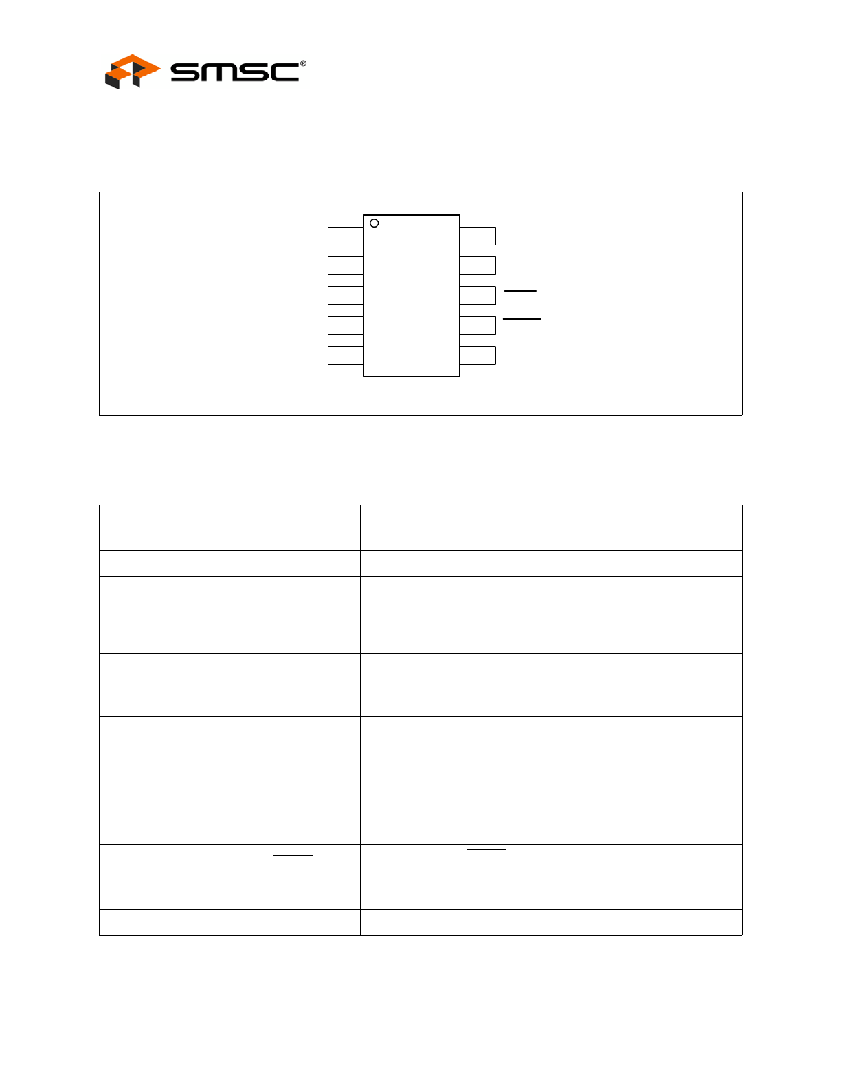
Chapter 2 Pin Description
The pin types are described below. All pins labelled with (5V) are 5V tolerant.
Figure 2.1 EMC1073/EMC1074 Pin Diagram, MSOP-10
Table 2.1 EMC1073 and EMC1074 Pin Description
PIN NUMBER
10-PIN
NAME
FUNCTION
TYPE
1
VDD
Power supply
Power
2
DP1
External diode 1 positive (anode)
connection
AIO
3
DN1
External diode 1 negative (cathode)
connection
AIO
4
DP2 / DN3
External diode 2 positive (anode)
connection / External Diode 3 negative
(cathode) connection for anti-parallel
diodes - EMC1074 only
AIO
5
DN2 / DP3
External diode 2 negative (cathode)
connection / External Diode 3 positive
(anode) connection for anti-parallel
diodes - EMC1074 only
AIO
6
GND
Ground Power
7
THERM / ADDR
Critical THERM output signal - requires
pull-up resistor to set SMBus Address
OD (5V)
8
ALERT
Active low digital ALERT output signal
- requires pull-up resistor
OD (5V)
9
SMDATA
SMBus Data input/output
DIOD (5V)
10
SMCLK
SMBus Clock input
DI (5V)
SMDATA
SMCLK
ALERT
VDD
DP1
DN1
DN2 / DP3
*
DP2 / DN3
*
THERM / ADDR
GND
1
2
3
4
5
10
9
8
7
6
* EMC1074 only

Multiple Channel 1°C Temperature Sensors with Selectable Address
Datasheet
SMSC EMC1073 / EMC1074
9
Revision 1.39 (10-11-10)
DATASHEET
APPLICATION NOTE: For the 5V tolerant pins that have a pull-up resistor (SMCLK, SMDATA, THERM, and
ALERT), the voltage difference between VDD and the pull-up voltage must never exceed
3.6V.
Power - these pins are used to supply either VDD or GND to the device.
AIO - Analog Input / Output.
DI - Digital Input.
OD - Open Drain Digital Output.
DIOD - Digital Input / Open Drain Output.

Multiple Channel 1°C Temperature Sensors with Selectable Address
Datasheet
Revision 1.39 (10-11-10)
10
SMSC EMC1073 / EMC1074
DATASHEET
Chapter 3 Electrical Specifications
3.1
Absolute Maximum Ratings
Note: Stresses at or above those listed could cause permanent damage to the device. This is a stress
rating only and functional operation of the device at any other condition above those indicated
in the operation sections of this specification is not implied. When powering this device from
laboratory or system power supplies, it is important that the Absolute Maximum Ratings not be
exceeded or device failure can result. Some power supplies exhibit voltage spikes on their
outputs when the AC power is switched on or off. In addition, voltage transients on the AC
power line may appear on the DC output. If this possibility exists, it is suggested that a clamp
circuit be used.
Note 3.1
For the 5V tolerant pins that have a pull-up resistor (SMCLK, SMDATA, THERM, and
ALERT), the pull-up voltage must not exceed 3.6V when the device is unpowered.
Table 3.1 Absolute Maximum Ratings
DESCRIPTION
RATING
UNIT
Supply Voltage (V
DD
)
-0.3 to 4.0
V
Voltage on 5V tolerant pins (V
5VT_pin
)
-0.3 to 5.5
V
Voltage on 5V tolerant pins (|V
5VT_pin
- V
DD
|) (see
Note 3.1
)
0 to 3.6
V
Voltage on any other pin to Ground
-0.3 to V
DD
+0.3
V
Operating Temperature Range
-40 to +125
°C
Storage Temperature Range
-55 to +150
°C
Lead Temperature Range
Refer to JEDEC Spec. J-STD-
020
Package Thermal Characteristics for MSOP-10
Thermal Resistance (
θ
j-a
)
132.2
°C/W
ESD Rating, All pins HBM
2000
V