
SMSC EMC1046/EMC1047
DATASHEET
Revision 0.69 (06-29-09)
Datasheet
PRODUCT FEATURES
EMC1046/EMC1047
1°C Multiple Temperature
Sensor with Beta
Compensation and
Hottest of Thermal Zones
General Description
The EMC1046/EMC1047are high accuracy, low cost,
System Management Bus (SMBus) temperature
sensors. Advanced features such as Resistance Error
Correction (REC), Beta Compensation (to CPU diodes
requiring the BJT or transistor model) and automatic
diode type detection combine to provide a robust
solution for complex envir onmental monitoring
applications.
Each device provides ±1° accuracy for external diode
temperatures and ±2°C accuracy for the internal diode
temperature. The EMC1046/EMC1047 monitor up to
seven temperature channels (up to six external and one
internal).
Applications
Notebook Computers
Desktop Computers
Industrial
Embedded Applications
Features
Designed to support 45nm, 65nm, and 90nm CPU
diodes
Supports diodes requiring the BJT or transistor model
Resistance Error Correction (up to 100 Ohms)
Up to six External Temperature Monitors
—
±1°C Accuracy (60°C < T
DIODE
< 100°C)
—
0.125°C Resolution
—
Supports up to 2.2nF filter capacitor
—
Anti-parallel diodes for extra diode support and
compact design
Internal Temperature Monitor
—
±2°C accuracy
3.3V Supply Voltage
Available in a 10-pin TSSOP lead-free RoHS
Compliant package
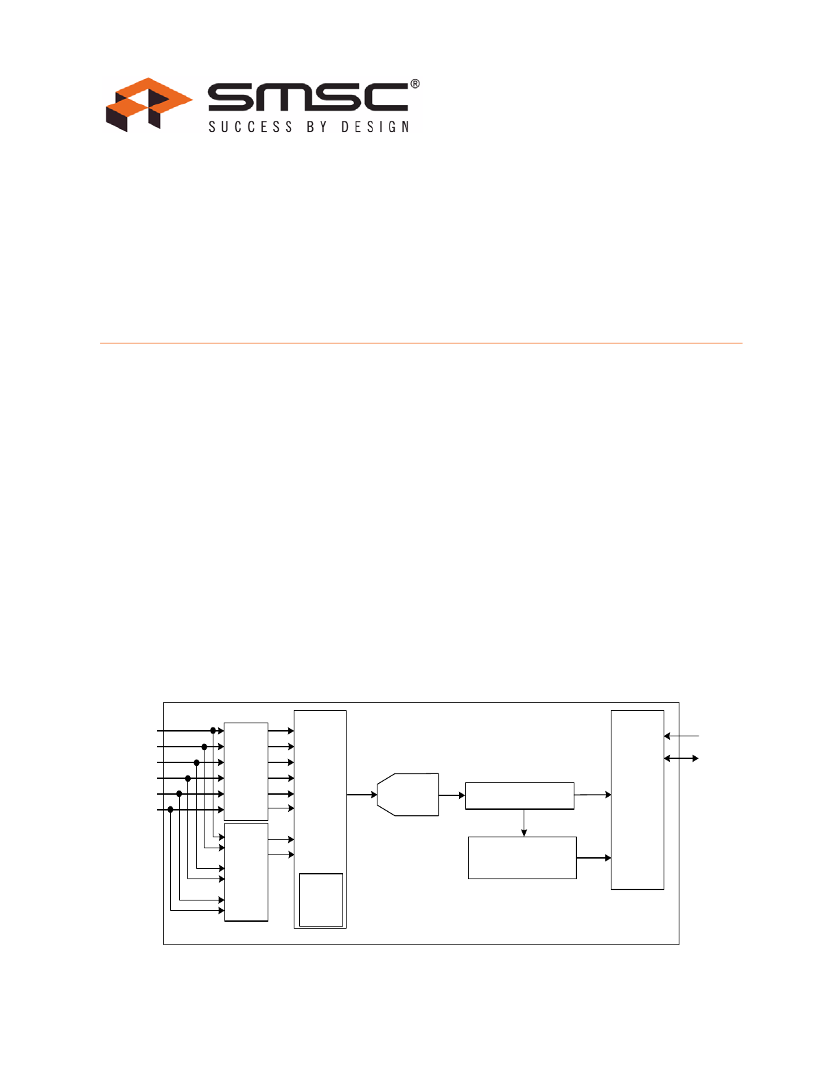
Block Diagram
Analog
Mux
External
Temp
Diodes
Internal
Temp
Diode
11 bit
Σ Δ
ADC
Temp Registers
SMBus
Slave
Protocol
DP1 / DN6*
DN1 / DP6*
SMCLK
SMDATA
DP2 / DN3
DN2 / DP3
DN4 / DP5
DP4 / DN5
Anti-
parallel
diode
* denotes EMC1047 only
Hottest of Comparison

ORDER NUMBERS:
Reel Size is 4,000 pieces
ORDERING NUMBER
PACKAGE
FEATURES
DIODE MODES
SUPPORTED
SMBUS
ADDRESS
EMC1046-1-AIZL-TR
10-pin TSSOP
(Lead-Free RoHS
Compliant)
Up to 5 external diodes. “Hottest Of”
temperature comparison
Intel CPU,
3904, AMD with
setup
1001_100(r/w)
EMC1046-6-AIZL-TR
10-pin TSSOP
(Lead-Free RoHS
Compliant)
Up to 5 external diodes. “Hottest Of”
temperature comparison
Intel CPU,
3904, AMD with
setup
1001_101(r/w)
EMC1047-1-AIZL-TR
10-pin TSSOP
(Lead-Free RoHS
Compliant)
Up to 6 external diodes. “Hottest Of”
temperature comparison
Intel CPU,
3904, AMD with
setup
1001_100(r/w)
EMC1047-2-AIZL-TR
10-pin TSSOP
(Lead-Free RoHS
Compliant)
Up to 6 external diodes. “Hottest Of”
temperature comparison
Intel CPU,
3904, AMD with
setup
1001_000(r/w)
1°C Multiple Temperature Sensor with Beta Compensation and Hottest of Thermal Zones
Datasheet
Revision 0.69 (06-29-09)
2
SMSC EMC1046/EMC1047
DATASHEET
80 ARKAY DRIVE, HAUPPAUGE, NY 11788 (631) 435-6000, FAX (631) 273-3123
Copyright © 2009 SMSC or its subsidiaries. All rights reserved.
Circuit diagrams and other information relating to SMSC products are included as a means of illustrating typical applications. Consequently, complete
information sufficient for construction purposes is not necessarily given. Although the information has been checked and is believed to be accurate,
no responsibility is assumed for inaccuracies. SMSC reserves the right to make changes to specifications and product descriptions at any time without
notice. Contact your local SMSC sales office to obtain the latest specifications before placing your product order. The provision of this information
does not convey to the purchaser of the described semiconductor devices any licenses under any patent rights or other intellectual property rights of
SMSC or others. All sales are expressly conditional on your agreement to the terms and conditions of the most recently dated version of SMSC's
standard Terms of Sale Agreement dated before the date of your order (the "Terms of Sale Agreement"). The product may contain design defects or
errors known as anomalies which may cause the product's functions to deviate from published specifications. Anomaly sheets are available upon
request. SMSC products are not designed, intended, authorized or warranted for use in any life support or other application where product failure
could cause or contribute to personal injury or severe property damage. Any and all such uses without prior written approval of an Officer of SMSC
and further testing and/or modification will be fully at the risk of the customer. Copies of this document or other SMSC literature, as well as the Terms
of Sale Agreement, may be obtained by visiting SMSC’s website at http://www.smsc.com. SMSC is a registered trademark of Standard Microsystems
Corporation (“SMSC”). Product names and company names are the trademarks of their respective holders.
SMSC DISCLAIMS AND EXCLUDES ANY AND ALL WARRANTIES, INCLUDING WITHOUT LIMITATION ANY AND ALL IMPLIED WARRANTIES
OF MERCHANTABILITY, FITNESS FOR A PARTICULAR PURPOSE, TITLE, AND AGAINST INFRINGEMENT AND THE LIKE, AND ANY AND ALL
WARRANTIES ARISING FROM ANY COURSE OF DEALING OR USAGE OF TRADE. IN NO EVENT SHALL SMSC BE LIABLE FOR ANY DIRECT,
INCIDENTAL, INDIRECT, SPECIAL, PUNITIVE, OR CONSEQUENTIAL DAMAGES; OR FOR LOST DATA, PROFITS, SAVINGS OR REVENUES OF
ANY KIND; REGARDLESS OF THE FORM OF ACTION, WHETHER BASED ON CONTRACT; TORT; NEGLIGENCE OF SMSC OR OTHERS;
STRICT LIABILITY; BREACH OF WARRANTY; OR OTHERWISE; WHETHER OR NOT ANY REMEDY OF BUYER IS HELD TO HAVE FAILED OF
ITS ESSENTIAL PURPOSE, AND WHETHER OR NOT SMSC HAS BEEN ADVISED OF THE POSSIBILITY OF SUCH DAMAGES.

1°C Multiple Temperature Sensor with Beta Compensation and Hottest of Thermal Zones
Datasheet
SMSC EMC1046/EMC1047
3
Revision 0.69 (06-29-09)
DATASHEET
Table of Contents
Chapter 1
Pin Description . . . . . . . . . . . . . . . . . . . . . . . . . . . . . . . . . . . . . . . . . . . . . . . . . . . . . 7
Chapter 2
Electrical Specifications . . . . . . . . . . . . . . . . . . . . . . . . . . . . . . . . . . . . . . . . . . . . . 9
2.1
Absolute Maximum Ratings . . . . . . . . . . . . . . . . . . . . . . . . . . . . . . . . . . . . . . . . . . . . . . . . . . . . . . . 9
2.2
Electrical Specifications . . . . . . . . . . . . . . . . . . . . . . . . . . . . . . . . . . . . . . . . . . . . . . . . . . . . . . . . . . 9
2.3
SMBus Electrical Characteristics . . . . . . . . . . . . . . . . . . . . . . . . . . . . . . . . . . . . . . . . . . . . . . . . . . 10
Chapter 3
System Management Bus Interface Protocol . . . . . . . . . . . . . . . . . . . . . . . . . . . 12
3.1
System Management Bus Interface Protocol . . . . . . . . . . . . . . . . . . . . . . . . . . . . . . . . . . . . . . . . . 12
3.2
Write Byte . . . . . . . . . . . . . . . . . . . . . . . . . . . . . . . . . . . . . . . . . . . . . . . . . . . . . . . . . . . . . . . . . . . . 12
3.3
Read Byte . . . . . . . . . . . . . . . . . . . . . . . . . . . . . . . . . . . . . . . . . . . . . . . . . . . . . . . . . . . . . . . . . . . . 13
3.4
Send Byte . . . . . . . . . . . . . . . . . . . . . . . . . . . . . . . . . . . . . . . . . . . . . . . . . . . . . . . . . . . . . . . . . . . . 13
3.5
Receive Byte. . . . . . . . . . . . . . . . . . . . . . . . . . . . . . . . . . . . . . . . . . . . . . . . . . . . . . . . . . . . . . . . . . 13
3.6
SMBus Address . . . . . . . . . . . . . . . . . . . . . . . . . . . . . . . . . . . . . . . . . . . . . . . . . . . . . . . . . . . . . . . 13
3.7
SMBus Timeout . . . . . . . . . . . . . . . . . . . . . . . . . . . . . . . . . . . . . . . . . . . . . . . . . . . . . . . . . . . . . . . 13
Chapter 4
Product Description . . . . . . . . . . . . . . . . . . . . . . . . . . . . . . . . . . . . . . . . . . . . . . . . 14
4.1
Modes of Operation . . . . . . . . . . . . . . . . . . . . . . . . . . . . . . . . . . . . . . . . . . . . . . . . . . . . . . . . . . . . 14
4.2
Temperature Monitoring . . . . . . . . . . . . . . . . . . . . . . . . . . . . . . . . . . . . . . . . . . . . . . . . . . . . . . . . . 15
4.2.1
Resistance Error Correction . . . . . . . . . . . . . . . . . . . . . . . . . . . . . . . . . . . . . . . . . . . . . . 15
4.2.2
Beta Compensation . . . . . . . . . . . . . . . . . . . . . . . . . . . . . . . . . . . . . . . . . . . . . . . . . . . . . 15
4.2.3
Digital Averaging . . . . . . . . . . . . . . . . . . . . . . . . . . . . . . . . . . . . . . . . . . . . . . . . . . . . . . . 15
4.2.4
“Hottest Of” Comparison . . . . . . . . . . . . . . . . . . . . . . . . . . . . . . . . . . . . . . . . . . . . . . . . . 15
4.2.5
Conversion Rates . . . . . . . . . . . . . . . . . . . . . . . . . . . . . . . . . . . . . . . . . . . . . . . . . . . . . . 16
4.2.6
Dynamic Averaging . . . . . . . . . . . . . . . . . . . . . . . . . . . . . . . . . . . . . . . . . . . . . . . . . . . . . 16
4.3
Diode Connections . . . . . . . . . . . . . . . . . . . . . . . . . . . . . . . . . . . . . . . . . . . . . . . . . . . . . . . . . . . . . 16
4.3.1
Diode Faults . . . . . . . . . . . . . . . . . . . . . . . . . . . . . . . . . . . . . . . . . . . . . . . . . . . . . . . . . . 17
Chapter 5
Register Description . . . . . . . . . . . . . . . . . . . . . . . . . . . . . . . . . . . . . . . . . . . . . . . 18
5.1
Data Read Interlock . . . . . . . . . . . . . . . . . . . . . . . . . . . . . . . . . . . . . . . . . . . . . . . . . . . . . . . . . . . . 22
5.2
Temperature Data Registers . . . . . . . . . . . . . . . . . . . . . . . . . . . . . . . . . . . . . . . . . . . . . . . . . . . . . 22
5.3
Status Register . . . . . . . . . . . . . . . . . . . . . . . . . . . . . . . . . . . . . . . . . . . . . . . . . . . . . . . . . . . . . . . . 23
5.4
Configuration Register . . . . . . . . . . . . . . . . . . . . . . . . . . . . . . . . . . . . . . . . . . . . . . . . . . . . . . . . . . 24
5.5
Conversion Rate Register. . . . . . . . . . . . . . . . . . . . . . . . . . . . . . . . . . . . . . . . . . . . . . . . . . . . . . . . 24
5.6
Limit Registers . . . . . . . . . . . . . . . . . . . . . . . . . . . . . . . . . . . . . . . . . . . . . . . . . . . . . . . . . . . . . . . . 25
5.7
One Shot Register . . . . . . . . . . . . . . . . . . . . . . . . . . . . . . . . . . . . . . . . . . . . . . . . . . . . . . . . . . . . . 27
5.8
External Diode Fault Register. . . . . . . . . . . . . . . . . . . . . . . . . . . . . . . . . . . . . . . . . . . . . . . . . . . . . 28
5.9
Consecutive ALERT Register . . . . . . . . . . . . . . . . . . . . . . . . . . . . . . . . . . . . . . . . . . . . . . . . . . . . . 28
5.10
Beta Configuration Register . . . . . . . . . . . . . . . . . . . . . . . . . . . . . . . . . . . . . . . . . . . . . . . . . . . . . . 29
5.11
Hottest Temperature Registers. . . . . . . . . . . . . . . . . . . . . . . . . . . . . . . . . . . . . . . . . . . . . . . . . . . . 30
5.12
Hottest Temperature Status Register . . . . . . . . . . . . . . . . . . . . . . . . . . . . . . . . . . . . . . . . . . . . . . . 31
5.13
High Limit Status Register . . . . . . . . . . . . . . . . . . . . . . . . . . . . . . . . . . . . . . . . . . . . . . . . . . . . . . . 31
5.14
Low Limit Status Register . . . . . . . . . . . . . . . . . . . . . . . . . . . . . . . . . . . . . . . . . . . . . . . . . . . . . . . . 32
5.15
REC Configuration Register . . . . . . . . . . . . . . . . . . . . . . . . . . . . . . . . . . . . . . . . . . . . . . . . . . . . . . 32
5.16
Hottest Configuration Register . . . . . . . . . . . . . . . . . . . . . . . . . . . . . . . . . . . . . . . . . . . . . . . . . . . . 33
5.17
Channel Configuration Register . . . . . . . . . . . . . . . . . . . . . . . . . . . . . . . . . . . . . . . . . . . . . . . . . . . 33
5.18
Filter Control Register. . . . . . . . . . . . . . . . . . . . . . . . . . . . . . . . . . . . . . . . . . . . . . . . . . . . . . . . . . . 34
5.19
Product ID Register . . . . . . . . . . . . . . . . . . . . . . . . . . . . . . . . . . . . . . . . . . . . . . . . . . . . . . . . . . . . 34
5.20
Manufacturer ID Register (FEh) . . . . . . . . . . . . . . . . . . . . . . . . . . . . . . . . . . . . . . . . . . . . . . . . . . . 35
5.21
Revision Register (FFh) . . . . . . . . . . . . . . . . . . . . . . . . . . . . . . . . . . . . . . . . . . . . . . . . . . . . . . . . . 35

1°C Multiple Temperature Sensor with Beta Compensation and Hottest of Thermal Zones
Datasheet
Revision 0.69 (06-29-09)
4
SMSC EMC1046/EMC1047
DATASHEET
Chapter 6
Package Information . . . . . . . . . . . . . . . . . . . . . . . . . . . . . . . . . . . . . . . . . . . . . . . 36
6.1
EMC1046/EMC1047 Package Drawing . . . . . . . . . . . . . . . . . . . . . . . . . . . . . . . . . . . . . . . . . . . . . 36
6.2
Package Markings . . . . . . . . . . . . . . . . . . . . . . . . . . . . . . . . . . . . . . . . . . . . . . . . . . . . . . . . . . . . . 36
6.2.1
EMC1046-X-AIZL (10-Pin TSSOP) . . . . . . . . . . . . . . . . . . . . . . . . . . . . . . . . . . . . . . . . . 36
Chapter 7
Revision History . . . . . . . . . . . . . . . . . . . . . . . . . . . . . . . . . . . . . . . . . . . . . . . . . . . 37

1°C Multiple Temperature Sensor with Beta Compensation and Hottest of Thermal Zones
Datasheet
SMSC EMC1046/EMC1047
5
Revision 0.69 (06-29-09)
DATASHEET
List of Figures
Figure 1.1 EMC1046/EMC1047 Pin Diagram . . . . . . . . . . . . . . . . . . . . . . . . . . . . . . . . . . . . . . . . . . . . . . 7
Figure 3.1 SMBus Timing Diagram . . . . . . . . . . . . . . . . . . . . . . . . . . . . . . . . . . . . . . . . . . . . . . . . . . . . . 12
Figure 4.1 System Diagram for EMC1046/EMC1047 . . . . . . . . . . . . . . . . . . . . . . . . . . . . . . . . . . . . . . . 14
Figure 4.2 Diode Connections. . . . . . . . . . . . . . . . . . . . . . . . . . . . . . . . . . . . . . . . . . . . . . . . . . . . . . . . . 17
Figure 6.1 10-Pin TSSOP Package Drawing . . . . . . . . . . . . . . . . . . . . . . . . . . . . . . . . . . . . . . . . . . . . . 36

1°C Multiple Temperature Sensor with Beta Compensation and Hottest of Thermal Zones
Datasheet
Revision 0.69 (06-29-09)
6
SMSC EMC1046/EMC1047
DATASHEET
List of Tables
Table 1.1 EMC1046/EMC1047 Pin Description. . . . . . . . . . . . . . . . . . . . . . . . . . . . . . . . . . . . . . . . . . . . . 7
Table 1.2 Pin Type. . . . . . . . . . . . . . . . . . . . . . . . . . . . . . . . . . . . . . . . . . . . . . . . . . . . . . . . . . . . . . . . . . . 8
Table 2.1 Absolute Maximum Ratings . . . . . . . . . . . . . . . . . . . . . . . . . . . . . . . . . . . . . . . . . . . . . . . . . . . . 9
Table 2.2 Electrical Specifications . . . . . . . . . . . . . . . . . . . . . . . . . . . . . . . . . . . . . . . . . . . . . . . . . . . . . . . 9
Table 2.3 SMBus Electrical Specifications . . . . . . . . . . . . . . . . . . . . . . . . . . . . . . . . . . . . . . . . . . . . . . . 10
Table 3.1 Protocol Format . . . . . . . . . . . . . . . . . . . . . . . . . . . . . . . . . . . . . . . . . . . . . . . . . . . . . . . . . . . . 12
Table 3.2 Write Byte Protocol . . . . . . . . . . . . . . . . . . . . . . . . . . . . . . . . . . . . . . . . . . . . . . . . . . . . . . . . . 12
Table 3.3 Read Byte Protocol . . . . . . . . . . . . . . . . . . . . . . . . . . . . . . . . . . . . . . . . . . . . . . . . . . . . . . . . . 13
Table 3.4 Send Byte Protocol . . . . . . . . . . . . . . . . . . . . . . . . . . . . . . . . . . . . . . . . . . . . . . . . . . . . . . . . . 13
Table 3.5 Receive Byte Protocol . . . . . . . . . . . . . . . . . . . . . . . . . . . . . . . . . . . . . . . . . . . . . . . . . . . . . . . 13
Table 4.1 Supply Current vs. Conversion Rate for EMC1046/EMC1047 . . . . . . . . . . . . . . . . . . . . . . . . 16
Table 5.1 Register Set in Hexadecimal Order . . . . . . . . . . . . . . . . . . . . . . . . . . . . . . . . . . . . . . . . . . . . . 18
Table 5.2 Temperature Data Registers . . . . . . . . . . . . . . . . . . . . . . . . . . . . . . . . . . . . . . . . . . . . . . . . . . 22
Table 5.3 Temperature Data Format . . . . . . . . . . . . . . . . . . . . . . . . . . . . . . . . . . . . . . . . . . . . . . . . . . . . 23
Table 5.4 Status Register . . . . . . . . . . . . . . . . . . . . . . . . . . . . . . . . . . . . . . . . . . . . . . . . . . . . . . . . . . . . 23
Table 5.5 Configuration Register . . . . . . . . . . . . . . . . . . . . . . . . . . . . . . . . . . . . . . . . . . . . . . . . . . . . . . . 24
Table 5.6 Conversion Rate Register . . . . . . . . . . . . . . . . . . . . . . . . . . . . . . . . . . . . . . . . . . . . . . . . . . . . 24
Table 5.7 Conversion Rate . . . . . . . . . . . . . . . . . . . . . . . . . . . . . . . . . . . . . . . . . . . . . . . . . . . . . . . . . . . 24
Table 5.8 Maximum Conversion Rate Per Temperature Channels . . . . . . . . . . . . . . . . . . . . . . . . . . . . . 25
Table 5.9 Temperature Limit Registers . . . . . . . . . . . . . . . . . . . . . . . . . . . . . . . . . . . . . . . . . . . . . . . . . . 25
Table 5.10 One Shot Register . . . . . . . . . . . . . . . . . . . . . . . . . . . . . . . . . . . . . . . . . . . . . . . . . . . . . . . . . . 27
Table 5.11 External Diode Fault Register . . . . . . . . . . . . . . . . . . . . . . . . . . . . . . . . . . . . . . . . . . . . . . . . . 28
Table 5.12 Consecutive ALERT Register . . . . . . . . . . . . . . . . . . . . . . . . . . . . . . . . . . . . . . . . . . . . . . . . . 28
Table 5.13 Consecutive Alert Settings. . . . . . . . . . . . . . . . . . . . . . . . . . . . . . . . . . . . . . . . . . . . . . . . . . . . 29
Table 5.14 Beta Configuration Register. . . . . . . . . . . . . . . . . . . . . . . . . . . . . . . . . . . . . . . . . . . . . . . . . . . 29
Table 5.15 Beta Compensation Look Up Table. . . . . . . . . . . . . . . . . . . . . . . . . . . . . . . . . . . . . . . . . . . . . 30
Table 5.16 Hottest Temperature Registers . . . . . . . . . . . . . . . . . . . . . . . . . . . . . . . . . . . . . . . . . . . . . . . . 30
Table 5.17 Hottest Temperature Register . . . . . . . . . . . . . . . . . . . . . . . . . . . . . . . . . . . . . . . . . . . . . . . . . 31
Table 5.18 High Limit Status Register . . . . . . . . . . . . . . . . . . . . . . . . . . . . . . . . . . . . . . . . . . . . . . . . . . . . 31
Table 5.19 Low Limit Status Register . . . . . . . . . . . . . . . . . . . . . . . . . . . . . . . . . . . . . . . . . . . . . . . . . . . . 32
Table 5.20 REC Configuration Register . . . . . . . . . . . . . . . . . . . . . . . . . . . . . . . . . . . . . . . . . . . . . . . . . . 32
Table 5.21 Hottest Configuration Register. . . . . . . . . . . . . . . . . . . . . . . . . . . . . . . . . . . . . . . . . . . . . . . . . 33
Table 5.22 Channel Configuration Register. . . . . . . . . . . . . . . . . . . . . . . . . . . . . . . . . . . . . . . . . . . . . . . . 33
Table 5.23 Filter Control Register . . . . . . . . . . . . . . . . . . . . . . . . . . . . . . . . . . . . . . . . . . . . . . . . . . . . . . . 34
Table 5.24 Product ID Register . . . . . . . . . . . . . . . . . . . . . . . . . . . . . . . . . . . . . . . . . . . . . . . . . . . . . . . . . 34
Table 5.25 Manufacturer ID Register. . . . . . . . . . . . . . . . . . . . . . . . . . . . . . . . . . . . . . . . . . . . . . . . . . . . . 35
Table 5.26 Revision Register. . . . . . . . . . . . . . . . . . . . . . . . . . . . . . . . . . . . . . . . . . . . . . . . . . . . . . . . . . . 35
Table 7.1 Customer Revision History . . . . . . . . . . . . . . . . . . . . . . . . . . . . . . . . . . . . . . . . . . . . . . . . . . . 37
1°C Multiple Temperature Sensor with Beta Compensation and Hottest of Thermal Zones
Datasheet
SMSC EMC1046/EMC1047
7
Revision 0.69 (06-29-09)
DATASHEET
Chapter 1 Pin Description
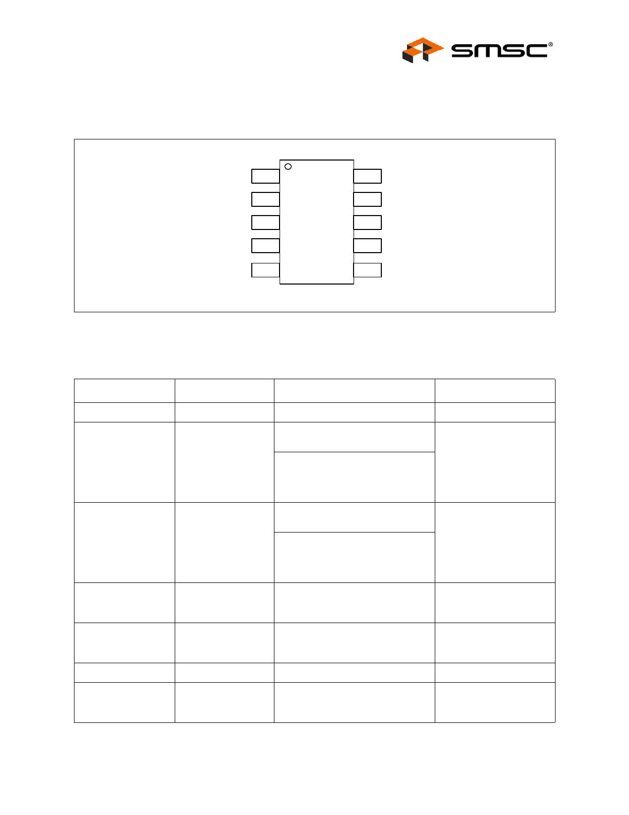
Figure 1.1 EMC1046/EMC1047 Pin Diagram
Table 1.1 EMC1046/EMC1047 Pin Description
PIN NUMBER
NAME
FUNCTION
TYPE
1
VDD
Power supply
Power
2
DP1 / DN6*
DP1 - External Diode 1 positive
(anode) connection (EMC1046)
AIO
DP1 / DN6 - External Diode 1
positive (anode) connection and
External Diode 6 negative (cathode)
connection (EMC1047)
3
DN1 / DP6*
DN1 - External diode 1 negative
(cathode) connection (EMC1046)
AIO
DN1 / DP6* - External diode 1
negative (cathode) connection and
External Diode 6 positive (anode)
connection (EMC1047)
4
DP2 / DN3
External Diode 2 positive (anode)
connection and External Diode 3
negative (cathode) connection
AIO
5
DN2 / DP3
External diode 2 negative (cathode)
connection and External Diode 3
positive (anode) connection
AIO
6
GND
Ground Connection
Power
7
DN4 / DP5
External diode 4 negative (cathode)
connection and External Diode 5
positive (anode) connection
AIO
EMC1046 / 7
10 TSSOP
10
9
8
7
SMDATA
SMCLK
1
2
3
4
VDD
DP1 / DN6*
DN1 / DP6*
GND
6
5
DP2 / DN3
DN2 / DP3
DP4 / DN5
DN4 / DP5
* denote EMC1047 only
1°C Multiple Temperature Sensor with Beta Compensation and Hottest of Thermal Zones
Datasheet
Revision 0.69 (06-29-09)
8
SMSC EMC1046/EMC1047
DATASHEET
The pin types are described below. All pins labelled (5V) are 5V tolerant.
APPLICATION NOTE: For the 5V tolerant pins that have a pull-up resistor, the voltage difference between VDD and
the pull-up voltage must never exceed 3.6V.
8
DP4 / DN5
External Diode 4 positive (anode)
connection and External Diode 5
negative (cathode) connection
AIO
9
SMDATA
SMBus Data input/output - requires
external pullup resistor
DIOD (5V)
10
SMCLK
SMBus Clock input - requires
external pullup resistor
DI (5V)
Table 1.2 Pin Type
PIN TYPE
FUNCTION
Power
Used to supply either VDD or GND to the device
DI
5V tolerant digital input
OD
5V tolerant Open drain digital output. Requires a pull-up resistor
DIOD
5V tolerant bi-directional digital input / open-drain output. Requires a pull-up
resistor.
AIO
Analog input / output used for external diodes or analog inputs
Table 1.1 EMC1046/EMC1047 Pin Description (continued)
PIN NUMBER
NAME
FUNCTION
TYPE
1°C Multiple Temperature Sensor with Beta Compensation and Hottest of Thermal Zones
Datasheet
SMSC EMC1046/EMC1047
9
Revision 0.69 (06-29-09)
DATASHEET
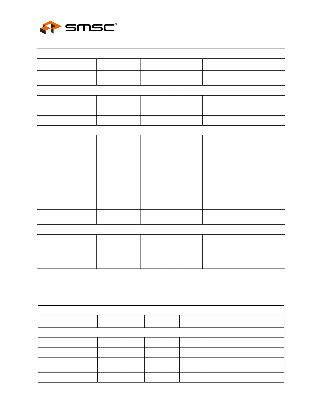
Chapter 2 Electrical Specifications
2.1
Absolute Maximum Ratings
Note: Stresses at or above those listed could cause permanent damage to the device. This is a stress
rating only and functional operation of the device at any other condition above those indicated
in the operation sections of this specification is not implied. When powering this device from
laboratory or system power supplies, it is important that the Absolute Maximum Ratings not be
exceeded or device failure can result. Some power supplies exhibit voltage spikes on their
outputs when the AC power is switched on or off. In addition, voltage transients on the AC
power line may appear on the DC output. If this possibility exists, it is suggested that a clamp
circuit be used.
Note 2.1
For the 5V tolerant pins that have a pull-up resistor, the pull-up voltage must not exceed
3.6V when the device is unpowered.
2.2
Electrical Specifications
Table 2.1 Absolute Maximum Ratings
DESCRIPTION
RATING
UNIT
Supply Voltage (V
DD
)
-0.3 to 4.0
V
Voltage on 5V tolerant pins (V
5VT_pin
)
-0.3 to 5.5
V
Voltage on 5V tolerant pins (|V
5VT_pin
- V
DD
|) (see
Note 2.1
)
-0.3 to 3.6
V
Voltage on any other pin to Ground
-0.3 to V
DD
+0.3
V
Operating Temperature Range
-40 to +125
°C
Storage Temperature Range
-55 to +150
°C
Lead Temperature Range
Refer to JEDEC Spec. J-STD-
020
Package Thermal Characteristics for MSOP-10
Thermal Resistance (
θ
j-a
)
132.2
°C/W
ESD Rating, All pins HBM
2000
V
Table 2.2 Electrical Specifications
V
DD
= 3.0V to 3.6V, T
A
= -40°C to 125°C, all typical values at T
A
= 27°C unless otherwise noted.
CHARACTERISTIC
SYMBOL
MIN
TYP
MAX
UNITS
CONDITIONS
DC Power
Supply Voltage
V
DD
3.0
3.3
3.6
V
Supply Current
I
DD
395
450
uA
1 conversion / sec, dynamic
averaging disabled
Supply Current
I
DD
700
960
uA
4 conversions / sec, dynamic
averaging enabled
1°C Multiple Temperature Sensor with Beta Compensation and Hottest of Thermal Zones
Datasheet
Revision 0.69 (06-29-09)
10
SMSC EMC1046/EMC1047
DATASHEET
2.3
SMBus Electrical Characteristics
Standby Supply Current
I
STBY
200
uA
RUN / STOP bit set. Monitoring
disabled.
Internal Temperature Monitor
Temperature Accuracy
±0.25
±1
°C
0°C < T
A
< 100°C
±2
°C
-40°C < T
A
< 125°C
Temperature Resolution
0.125
°C
External Temperature Monitor
Temperature Accuracy
±0.25
±1
°C
+40°C < T
DIODE
< +110°C
0°C < T
A
< 110°C
±0.5
±2
°C
-40°C < T
DIODE
< 127°C
Temperature Resolution
0.125
°C
Conversion Time all
Channels
t
CONV
190
ms
default settings
Capacitive Filter
C
FILTER
2.2
2.7
nF
Connected across external diode
Resistance Error
Correction
R
SERIES
100
Ω
In series with DP and DN lines
Leakage Current
I
LEAK
±5
uA
powered or unpowered
T
A
< 85°C
Power Up Timing
First conversion ready
t
CONV_f
300
ms
Time after power up before all
channels updated with valid data
SMBus delay
t
SMB_d
15
ms
Delay before SMBus
communications should be sent by
host
Table 2.3 SMBus Electrical Specifications
V
DD
= 3.0V to 3.6V, T
A
= -40°C to 125°C, all typical values are at T
A
= 27°C unless otherwise noted.
CHARACTERISTIC
SYMBOL
MIN
TYP
MAX
UNITS
CONDITIONS
SMBus Interface
Input High Voltage
V
IH
2.0
V
DD
V
5V Tolerant
Input Low Voltage
V
IL
-0.3
0.8
V
5V Tolerant
Input High/Low Current
I
IH /
I
IL
±5
uA
Powered or unpowered
T
A
< 85°C
Hysteresis
420
mV
Table 2.2 Electrical Specifications (continued)
V
DD
= 3.0V to 3.6V, T
A
= -40°C to 125°C, all typical values at T
A
= 27°C unless otherwise noted.
CHARACTERISTIC
SYMBOL
MIN
TYP
MAX
UNITS
CONDITIONS