
SMSC EMC1043
DATASHEET
Revision 1.44 (04-14-08)
Datasheet
PRODUCT FEATURES
EMC1043
1°C Triple Temperature
Sensor with Beta
Compensation and
Hotter of Two Zones
General Description
The EMC1043 is a family of System Management Bus
(SMBus) temperature sensors that monitors three
temperature zones, one internal diode and two
externally connected diodes, for PC and embedded
e n v i r o n m e n t s . T h e E M C 1 0 4 3 i n c l u d e s b e t a
compensation circuitry to correct for variation in the beta
of measurement transistors. Other extended features
include resistance error correction and ideality factor
configuration to eliminate major sources of temperature
measurement error.
1
An added feature to the EMC1043 is a function that
automatically compares the two external temperature
zones and reports the hotter of the two temperatures.
Selectable conversion rates and standby mode support
low-power operation. The temperature measurement
ranges support two data ranges (and formats), -64°C to
+127°C and -64°C to +191°C.
Applications
Desktop and Notebook Computers
Hardware Management
Servers
Embedded Applications
Features
Supports two External Temperature Diodes
—
±1°C Accuracy (40°C to 80°C)
—
0.125
°C Resolution
—
Ideality Factor Configuration
—
Accepts 2200pF Cap Across External Diodes for Noise
Suppression
—
Optional Resistive Error Correction on External Diode 2
—
Resistance Error Correction (up to 100 Ohms)
—
Beta Compensation
Internal Temperature Diode
—
±3°C Accuracy (0°C to 85°C)
—
0.125
°C Resolution
Low Power Operation
—
4uA Standby Current
3.0V to 3.6V Supply
Programmable Conversion Rate
SMBus 2.0 Compliant
—
Four SMBus Address Available
Reports Hotter of Two Diodes with Dual-core CPU
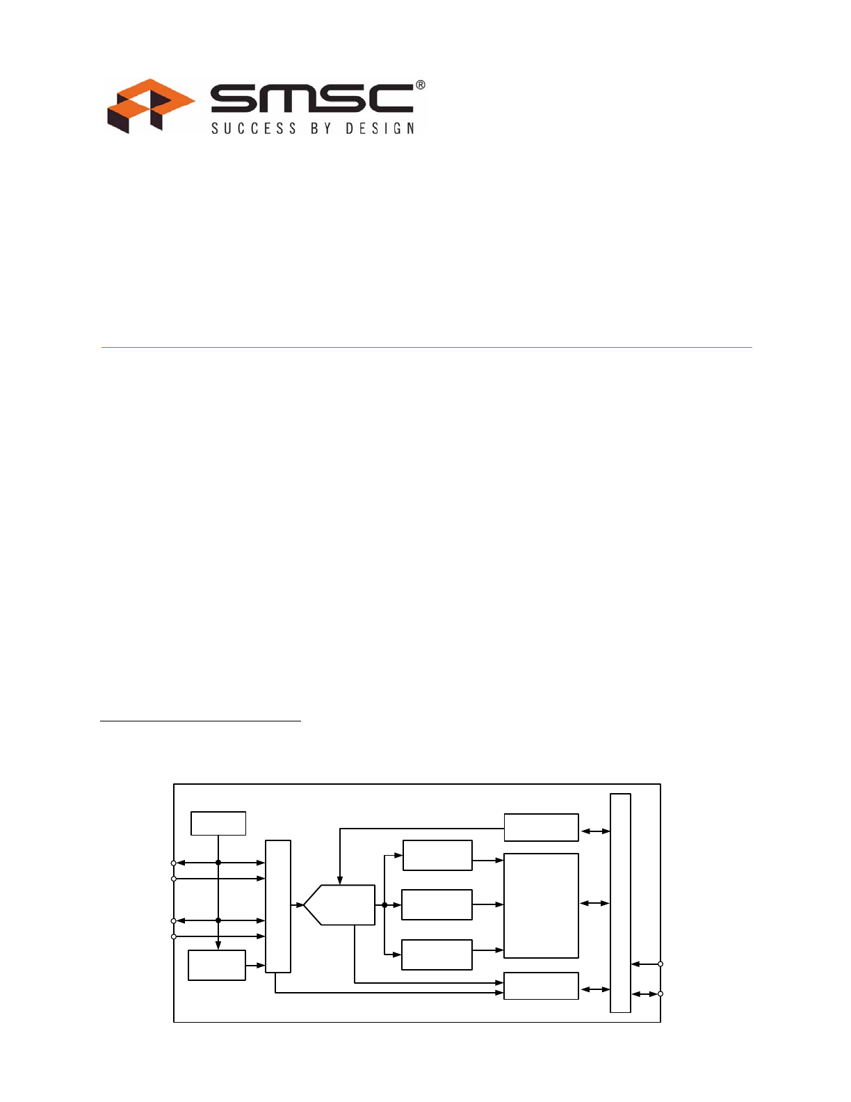
Simplified Block Diagram
1.Patents pending
Local Temp
Diode
Switching
Current
SMCLK
Internal Diode
Register
Configuration
Register
Status Register
S
M
Bu
s
Inte
rf
ac
e
External Diode
1 Register
External Diode
2 Register
SMDATA
11-bit
delta-sigma
ADC
An
al
og
M
u
x
an
d
A
n
ti
-A
lia
s
F
ilt
er
DP1
DN1
DP2
DN2
Digital Mux
and
Byte Interlock
Reel size is 4,000 pieces.
Evaluation Boards available upon request. (EVB-EMC1043, EVB-EMC1043C)
ORDERING NUMBER
PACKAGE
FEATURES
SMBUS ADDRESS
EMC1043-1-ACZL-TR
8 pinMSOP package
(Lead Free ROHS
compliant)
Two external diodes with
REC and Beta
Compensation and Hottest
Of Comparision
1001_100x
EMC1043-2-ACZL-TR
1001_101x
EMC1043-3-ACZL-TR
1001_000x
EMC1043-4-ACZL-TR
1001_001x
EMC1043-5-ACZL-TR
Two external diodes with
REC. Beta Compensation
on External Diode 1 only.
Hottest of Comparision
1001_100x
1°C Triple Temperature Sensor with Beta Compensation and Hotter of Two Zones
Datasheet
Revision 1.44 (04-14-08)
2
SMSC EMC1043
DATASHEET
80 ARKAY DRIVE, HAUPPAUGE, NY 11788 (631) 435-6000, FAX (631) 273-3123
Copyright © 2008 SMSC or its subsidiaries. All rights reserved.
Circuit diagrams and other information relating to SMSC products are included as a means of illustrating typical applications. Consequently, complete information sufficient for
construction purposes is not necessarily given. Although the information has been checked and is believed to be accurate, no responsibility is assumed for inaccuracies. SMSC
reserves the right to make changes to specifications and product descriptions at any time without notice. Contact your local SMSC sales office to obtain the latest specifications
before placing your product order. The provision of this information does not convey to the purchaser of the described semiconductor devices any licenses under any patent
rights or other intellectual property rights of SMSC or others. All sales are expressly conditional on your agreement to the terms and conditions of the most recently dated
version of SMSC's standard Terms of Sale Agreement dated before the date of your order (the "Terms of Sale Agreement"). The product may contain design defects or errors
known as anomalies which may cause the product's functions to deviate from published specifications. Anomaly sheets are available upon request. SMSC products are not
designed, intended, authorized or warranted for use in any life support or other application where product failure could cause or contribute to personal injury or severe property
damage. Any and all such uses without prior written approval of an Officer of SMSC and further testing and/or modification will be fully at the risk of the customer. Copies of
this document or other SMSC literature, as well as the Terms of Sale Agreement, may be obtained by visiting SMSC’s website at http://www.smsc.com. SMSC is a registered
trademark of Standard Microsystems Corporation (“SMSC”). Product names and company names are the trademarks of their respective holders.
SMSC DISCLAIMS AND EXCLUDES ANY AND ALL WARRANTIES, INCLUDING WITHOUT LIMITATION ANY AND ALL IMPLIED WARRANTIES OF MERCHANTABILITY,
FITNESS FOR A PARTICULAR PURPOSE, TITLE, AND AGAINST INFRINGEMENT AND THE LIKE, AND ANY AND ALL WARRANTIES ARISING FROM ANY COURSE
OF DEALING OR USAGE OF TRADE. IN NO EVENT SHALL SMSC BE LIABLE FOR ANY DIRECT, INCIDENTAL, INDIRECT, SPECIAL, PUNITIVE, OR CONSEQUENTIAL
DAMAGES; OR FOR LOST DATA, PROFITS, SAVINGS OR REVENUES OF ANY KIND; REGARDLESS OF THE FORM OF ACTION, WHETHER BASED ON CONTRACT;
TORT; NEGLIGENCE OF SMSC OR OTHERS; STRICT LIABILITY; BREACH OF WARRANTY; OR OTHERWISE; WHETHER OR NOT ANY REMEDY OF BUYER IS HELD
TO HAVE FAILED OF ITS ESSENTIAL PURPOSE, AND WHETHER OR NOT SMSC HAS BEEN ADVISED OF THE POSSIBILITY OF SUCH DAMAGES.
ORDERING INFORMATION

1°C Triple Temperature Sensor with Beta Compensation and Hotter of Two Zones
Datasheet
SMSC EMC1043
3
Revision 1.44 (04-14-08)
DATASHEET
Table of Contents
Chapter 1
Pin Function . . . . . . . . . . . . . . . . . . . . . . . . . . . . . . . . . . . . . . . . . . . . . . . . . . . . . . . 6
Chapter 2
Electrical Specifications . . . . . . . . . . . . . . . . . . . . . . . . . . . . . . . . . . . . . . . . . . . . . 7
2.1
Absolute Maximum Ratings . . . . . . . . . . . . . . . . . . . . . . . . . . . . . . . . . . . . . . . . . . . . . . . . . . . . . . . 7
2.2
Electrical Specifications . . . . . . . . . . . . . . . . . . . . . . . . . . . . . . . . . . . . . . . . . . . . . . . . . . . . . . . . . . 7
2.3
System Management Bus Interface Protocol . . . . . . . . . . . . . . . . . . . . . . . . . . . . . . . . . . . . . . . . . . 9
2.3.1
Write Byte . . . . . . . . . . . . . . . . . . . . . . . . . . . . . . . . . . . . . . . . . . . . . . . . . . . . . . . . . . . . . 9
2.3.2
Read Byte . . . . . . . . . . . . . . . . . . . . . . . . . . . . . . . . . . . . . . . . . . . . . . . . . . . . . . . . . . . . . 9
2.3.3
Send Byte . . . . . . . . . . . . . . . . . . . . . . . . . . . . . . . . . . . . . . . . . . . . . . . . . . . . . . . . . . . . 10
2.3.4
Receive Byte . . . . . . . . . . . . . . . . . . . . . . . . . . . . . . . . . . . . . . . . . . . . . . . . . . . . . . . . . . 10
2.3.5
SMBus Timing Diagram. . . . . . . . . . . . . . . . . . . . . . . . . . . . . . . . . . . . . . . . . . . . . . . . . . 10
2.4
SMBus Addresses . . . . . . . . . . . . . . . . . . . . . . . . . . . . . . . . . . . . . . . . . . . . . . . . . . . . . . . . . . . . . 10
2.5
SMBus Timeout . . . . . . . . . . . . . . . . . . . . . . . . . . . . . . . . . . . . . . . . . . . . . . . . . . . . . . . . . . . . . . . 10
Chapter 3
Product Description . . . . . . . . . . . . . . . . . . . . . . . . . . . . . . . . . . . . . . . . . . . . . . . . 11
3.1
Power Modes . . . . . . . . . . . . . . . . . . . . . . . . . . . . . . . . . . . . . . . . . . . . . . . . . . . . . . . . . . . . . . . . . 11
3.2
One Shot During Standby Mode. . . . . . . . . . . . . . . . . . . . . . . . . . . . . . . . . . . . . . . . . . . . . . . . . . . 11
3.3
Operation During Run Mode. . . . . . . . . . . . . . . . . . . . . . . . . . . . . . . . . . . . . . . . . . . . . . . . . . . . . . 12
3.3.1
Conversion Rates . . . . . . . . . . . . . . . . . . . . . . . . . . . . . . . . . . . . . . . . . . . . . . . . . . . . . . 12
3.3.2
Dynamic Averaging . . . . . . . . . . . . . . . . . . . . . . . . . . . . . . . . . . . . . . . . . . . . . . . . . . . . . 12
3.4
Temperature Monitors . . . . . . . . . . . . . . . . . . . . . . . . . . . . . . . . . . . . . . . . . . . . . . . . . . . . . . . . . . 13
3.5
Temperature Measurement Results and Data . . . . . . . . . . . . . . . . . . . . . . . . . . . . . . . . . . . . . . . . 14
3.6
Resistance Error Correction (REC) . . . . . . . . . . . . . . . . . . . . . . . . . . . . . . . . . . . . . . . . . . . . . . . . 15
3.7
Beta Compensation . . . . . . . . . . . . . . . . . . . . . . . . . . . . . . . . . . . . . . . . . . . . . . . . . . . . . . . . . . . . 15
3.8
Programmable Ideality Factor. . . . . . . . . . . . . . . . . . . . . . . . . . . . . . . . . . . . . . . . . . . . . . . . . . . . . 16
3.9
Diode Faults . . . . . . . . . . . . . . . . . . . . . . . . . . . . . . . . . . . . . . . . . . . . . . . . . . . . . . . . . . . . . . . . . . 16
Chapter 4
Register Set and Description. . . . . . . . . . . . . . . . . . . . . . . . . . . . . . . . . . . . . . . . . 17
4.1
Legacy Temperature Data Registers (00h, 23h, 01h, 10h, F8h, F9h) . . . . . . . . . . . . . . . . . . . . . . 19
4.2
Extended Format Temperature Registers (FAh-FDh) . . . . . . . . . . . . . . . . . . . . . . . . . . . . . . . . . . 19
4.3
Status Register - 02h . . . . . . . . . . . . . . . . . . . . . . . . . . . . . . . . . . . . . . . . . . . . . . . . . . . . . . . . . . . 20
4.4
Configuration Register (03h Read, 09h Write) . . . . . . . . . . . . . . . . . . . . . . . . . . . . . . . . . . . . . . . . 20
4.5
Configuration 2 Register - (04h) . . . . . . . . . . . . . . . . . . . . . . . . . . . . . . . . . . . . . . . . . . . . . . . . . . . 21
4.6
One Shot Register - (0Fh) . . . . . . . . . . . . . . . . . . . . . . . . . . . . . . . . . . . . . . . . . . . . . . . . . . . . . . . 22
4.7
Ideality Configuration Registers (27h - 28h) . . . . . . . . . . . . . . . . . . . . . . . . . . . . . . . . . . . . . . . . . . 22
4.8
Beta Configuration Registers (29h - 2Ah). . . . . . . . . . . . . . . . . . . . . . . . . . . . . . . . . . . . . . . . . . . . 24
4.9
Product ID Register (EDh) . . . . . . . . . . . . . . . . . . . . . . . . . . . . . . . . . . . . . . . . . . . . . . . . . . . . . . . 25
4.10
Manufacturer ID Register (FEh) . . . . . . . . . . . . . . . . . . . . . . . . . . . . . . . . . . . . . . . . . . . . . . . . . . . 25
4.11
Revision Register (FFh) . . . . . . . . . . . . . . . . . . . . . . . . . . . . . . . . . . . . . . . . . . . . . . . . . . . . . . . . . 25
Chapter 5
Typical Operating Curves. . . . . . . . . . . . . . . . . . . . . . . . . . . . . . . . . . . . . . . . . . . 26
Chapter 6
Package Outline . . . . . . . . . . . . . . . . . . . . . . . . . . . . . . . . . . . . . . . . . . . . . . . . . . . 28
6.1
Package Markings . . . . . . . . . . . . . . . . . . . . . . . . . . . . . . . . . . . . . . . . . . . . . . . . . . . . . . . . . . . . . 29

1°C Triple Temperature Sensor with Beta Compensation and Hotter of Two Zones
Datasheet
Revision 1.44 (04-14-08)
4
SMSC EMC1043
DATASHEET
List of Figures
Figure 1.1 EMC1043 Pin Diagram . . . . . . . . . . . . . . . . . . . . . . . . . . . . . . . . . . . . . . . . . . . . . . . . . . . . . . 6
Figure 2.1 System Management Bus Timing Diagram . . . . . . . . . . . . . . . . . . . . . . . . . . . . . . . . . . . . . . . 9
Figure 3.1 EMC1043 System Drawing . . . . . . . . . . . . . . . . . . . . . . . . . . . . . . . . . . . . . . . . . . . . . . . . . . 11
Figure 3.2 Block Diagram of Temperature Monitoring Circuit . . . . . . . . . . . . . . . . . . . . . . . . . . . . . . . . . 13
Figure 3.3 External Diode Configurations . . . . . . . . . . . . . . . . . . . . . . . . . . . . . . . . . . . . . . . . . . . . . . . . 14
Figure 6.1 8-Pin MSOP Package Outline - 3x3mm Body 0.65mm Pitch. . . . . . . . . . . . . . . . . . . . . . . . . 28

1°C Triple Temperature Sensor with Beta Compensation and Hotter of Two Zones
Datasheet
SMSC EMC1043
5
Revision 1.44 (04-14-08)
DATASHEET
List of Tables
Table 1.1 EMC1043 Pin Description . . . . . . . . . . . . . . . . . . . . . . . . . . . . . . . . . . . . . . . . . . . . . . . . . . . . . 6
Table 2.1 Absolute Maximum Ratings . . . . . . . . . . . . . . . . . . . . . . . . . . . . . . . . . . . . . . . . . . . . . . . . . . . . 7
Table 2.2 Electrical Characteristics . . . . . . . . . . . . . . . . . . . . . . . . . . . . . . . . . . . . . . . . . . . . . . . . . . . . . . 7
Table 2.3 Write Byte Protocol . . . . . . . . . . . . . . . . . . . . . . . . . . . . . . . . . . . . . . . . . . . . . . . . . . . . . . . . . . 9
Table 2.4 Read Byte Protocol . . . . . . . . . . . . . . . . . . . . . . . . . . . . . . . . . . . . . . . . . . . . . . . . . . . . . . . . . . 9
Table 2.5 Send Byte Protocol . . . . . . . . . . . . . . . . . . . . . . . . . . . . . . . . . . . . . . . . . . . . . . . . . . . . . . . . . 10
Table 2.6 Receive Byte Protocol . . . . . . . . . . . . . . . . . . . . . . . . . . . . . . . . . . . . . . . . . . . . . . . . . . . . . . . 10
Table 3.1 Supply Current vs. Conversion Rate and ADC Averaging Factor . . . . . . . . . . . . . . . . . . . . . . 12
Table 3.2 EMC1043 Temperature Data Format . . . . . . . . . . . . . . . . . . . . . . . . . . . . . . . . . . . . . . . . . . . 15
Table 4.1 EMC1043 Register Set . . . . . . . . . . . . . . . . . . . . . . . . . . . . . . . . . . . . . . . . . . . . . . . . . . . . . . 17
Table 4.2 Status Register . . . . . . . . . . . . . . . . . . . . . . . . . . . . . . . . . . . . . . . . . . . . . . . . . . . . . . . . . . . . 20
Table 4.3 Configuration Register . . . . . . . . . . . . . . . . . . . . . . . . . . . . . . . . . . . . . . . . . . . . . . . . . . . . . . . 20
Table 4.4 Conversion Rate . . . . . . . . . . . . . . . . . . . . . . . . . . . . . . . . . . . . . . . . . . . . . . . . . . . . . . . . . . . 21
Table 4.5 Configuration 2 Register . . . . . . . . . . . . . . . . . . . . . . . . . . . . . . . . . . . . . . . . . . . . . . . . . . . . . 21
Table 4.6 One Shot Registers . . . . . . . . . . . . . . . . . . . . . . . . . . . . . . . . . . . . . . . . . . . . . . . . . . . . . . . . . 22
Table 4.7 Ideality Configuration Registers. . . . . . . . . . . . . . . . . . . . . . . . . . . . . . . . . . . . . . . . . . . . . . . . 22
Table 4.8 Ideality Factor Look Up Table . . . . . . . . . . . . . . . . . . . . . . . . . . . . . . . . . . . . . . . . . . . . . . . . . 23
Table 4.9 Substrate Diode Ideality Factor Look-Up Table (BJT Model) . . . . . . . . . . . . . . . . . . . . . . . . . 23
Table 4.10 Beta Configuration Registers. . . . . . . . . . . . . . . . . . . . . . . . . . . . . . . . . . . . . . . . . . . . . . . . . . 24
Table 4.11 Beta Configuration Look Up Table. . . . . . . . . . . . . . . . . . . . . . . . . . . . . . . . . . . . . . . . . . . . . . 24
Table 4.12 Product ID Register . . . . . . . . . . . . . . . . . . . . . . . . . . . . . . . . . . . . . . . . . . . . . . . . . . . . . . . . . 25
Table 4.13 Manufacturer ID Register. . . . . . . . . . . . . . . . . . . . . . . . . . . . . . . . . . . . . . . . . . . . . . . . . . . . . 25
Table 4.14 Revision Register. . . . . . . . . . . . . . . . . . . . . . . . . . . . . . . . . . . . . . . . . . . . . . . . . . . . . . . . . . . 25
Table 6.1 8-Pin MSOP Package Parameters . . . . . . . . . . . . . . . . . . . . . . . . . . . . . . . . . . . . . . . . . . . . . 28
1°C Triple Temperature Sensor with Beta Compensation and Hotter of Two Zones
Datasheet
Revision 1.44 (04-14-08)
6
SMSC EMC1043
DATASHEET
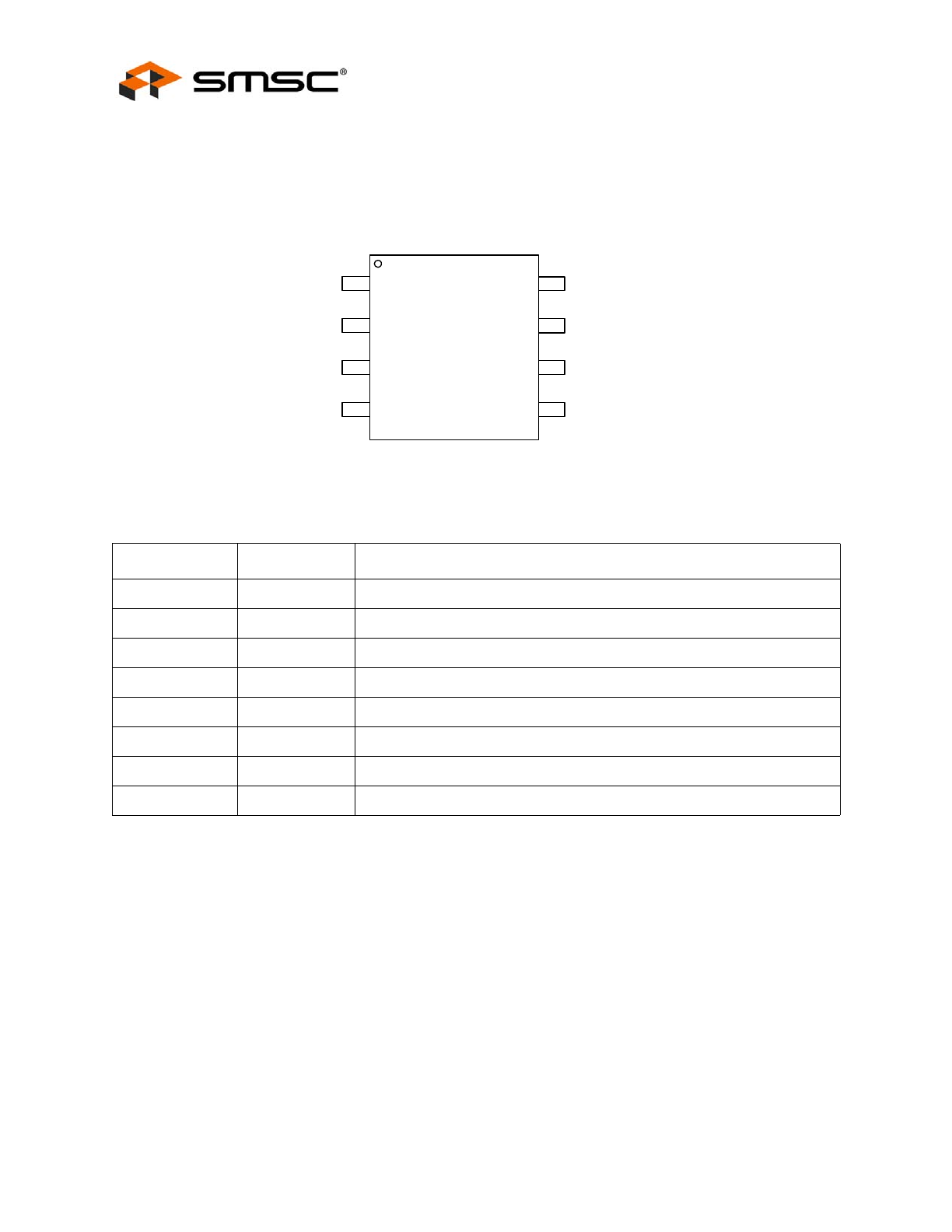
Chapter 1 Pin Function
Figure 1.1 EMC1043 Pin Diagram
Table 1.1 EMC1043 Pin Description
PIN
PIN NO.
DESCRIPTION
DP1
1
External Diode 1 Positive (anode) Connection
DN1
2
External Diode 1 Negative (cathode) Connection
DP2
3
External Diode 2 Positive (anode) Connection
DN2
4
External Diode 2 Negative (cathode) Connection
GND
5
Ground
VDD
6
Supply Voltage
SMDATA
7
System Management Bus Data - bi-directional data, open drain output
SMCLK
8
System Management Bus Clock Input
8-MSOP
8
7
6
5
1
2
3
4
DP1
DN1
DP2
DN2
SMCLK
SMDATA
VDD
GND
1°C Triple Temperature Sensor with Beta Compensation and Hotter of Two Zones
Datasheet
SMSC EMC1043
7
Revision 1.44 (04-14-08)
DATASHEET
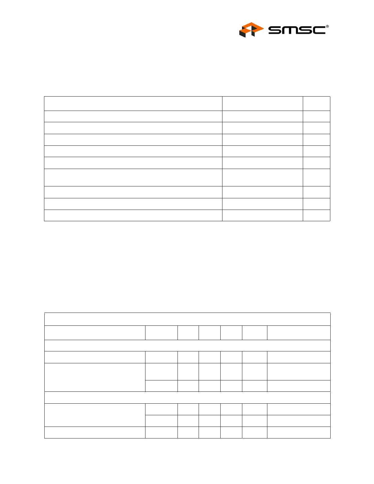
Chapter 2 Electrical Specifications
2.1
Absolute Maximum Ratings
Note: Stresses above those listed could cause damage to the device. This is a stress rating only and
functional operation of the device at any other condition above those indicated in the operation
sections of this specification is not implied. When powering this device from laboratory or
system power supplies, it is important that the Absolute Maximum Ratings not be exceeded or
device failure can result. Some power supplies exhibit voltage spikes on their outputs when the
AC power is switched on or off. In addition, voltage transients on the AC power line may appear
on the DC output. If this possibility exists, it is suggested that a clamp circuit be used.
2.2
Electrical Specifications
Table 2.1 Absolute Maximum Ratings
DESCRIPTION
RATING
UNIT
Supply Voltage V
DD
-0.3 to 5.0
V
Voltage on SMDATA and SMCLK
pins
-0.3 to 5.5
V
Voltage on any other pin
-0.3 to VDD+0.3
V
Operating Temperature Range
-40 to 125
°C
Storage Temperature Range
-55 to 150
°C
Lead Temperature Range
Refer to JEDEC
Spec. J-STD-020
Package Thermal Characteristics for MSOP-8
Thermal Resistance T
JA
(at 0 air flow)
135.9
°C/W
ESD Rating, All Pins Human Body Model
2000
V
Table 2.2 Electrical Characteristics
V
DD
=3.0V to 3.6V, T
A
= -20
°C to +85°C, Typical values at T
A
= 27
°C unless otherwise noted
PARAMETER
SYMBOL
MIN
TYP
MAX
UNITS
CONDITIONS
DC Power
Supply Voltage
V
DD
3.0
3.3
3.6
V
Average Operating Current
I
DD
340
400
μA
4 conversions/s
See
Table 4.4
.
I
STBY
2
4
μA
Standby mode
Internal Temperature Monitor
Temperature Accuracy
± 1
± 3
°C
-20
°C≤ T
A
≤85°C
± 1.5
°C
0
°C < T
A
≤ 85°C
Temperature Resolution
0.125
°C

1°C Triple Temperature Sensor with Beta Compensation and Hotter of Two Zones
Datasheet
Revision 1.44 (04-14-08)
8
SMSC EMC1043
DATASHEET
External Temperature Monitor
Temperature Accuracy
Remote Diode 40
°C to 80°C
Remote Diode -20
°C to 125°C
Remote Diode -64
°C to 192°C
± 1
± 3
± 5
°C
°C
°C
15
°C≤T
A
≤70°C
-20
°C≤T
A
≤85°C
-20
°C≤T
A
≤85°C
Temperature Resolution
0.125
°C
Filter Capacitor
C
FILTER
2.2
nF
Connected across
external diode
Note 2.2
Voltage Tolerance
Voltage at pin (
SMDATA,SMCLK)
V
TOL
-0.3
5.5
V
SMBus Interface (SMDATA,SMCLK)
Input High Level
V
IH
2.0
V
Input Low Level
V
IL
0.8
V
Input High/Low Current
I
IH
/I
IL
-1
1
μ
A
Hysteresis
500
mV
Input Capacitance
5
pF
Output Low Sink Current
6
mA
SMDATA = 0.6V
SMBus Timing
Clock Frequency
F
SMB
10
400
kHz
Spike Suppression
50
ns
Bus free time Start to Stop
T
BUF
1.3
μ
s
Hold time Start
T
HD:STA
0.6
μ
s
Setup time Start
T
SU:STA
0.6
μ
s
Setup time Stop
T
SU:STO
0.6
μ
s
Data Hold Time
T
HD:DAT
0.3
μ
s
Data Setup Time
T
SU:DAT
100
ns
Clock Low Period
T
LOW
1.3
μ
s
Clock High Period
T
HIGH
0.6
μ
s
Clock/Data Fall Time
T
F
*
300
ns
*Min = 20+0.1C
b
ns
Clock/Data Rise Time
T
R
*
300
Note
2.1
ns
*Min = 20+0.1C
b
ns
Capacitive Load (each bus line)
C
b
0.6
400
pF
Table 2.2 Electrical Characteristics (continued)
V
DD
=3.0V to 3.6V, T
A
= -20
°C to +85°C, Typical values at T
A
= 27
°C unless otherwise noted
PARAMETER
SYMBOL
MIN
TYP
MAX
UNITS
CONDITIONS
1°C Triple Temperature Sensor with Beta Compensation and Hotter of Two Zones
Datasheet
SMSC EMC1043
9
Revision 1.44 (04-14-08)
DATASHEET
Note 2.1
300nS rise time max is required for 400kHz bus operation. For lower clock frequencies,
the maximum rise time is (0.1/F
SMB
)+50nS
Note 2.2
See SMSC Applications for Application Notes and Guidelines when measuring GPU
processor diodes and CPU processor diodes.
2.3
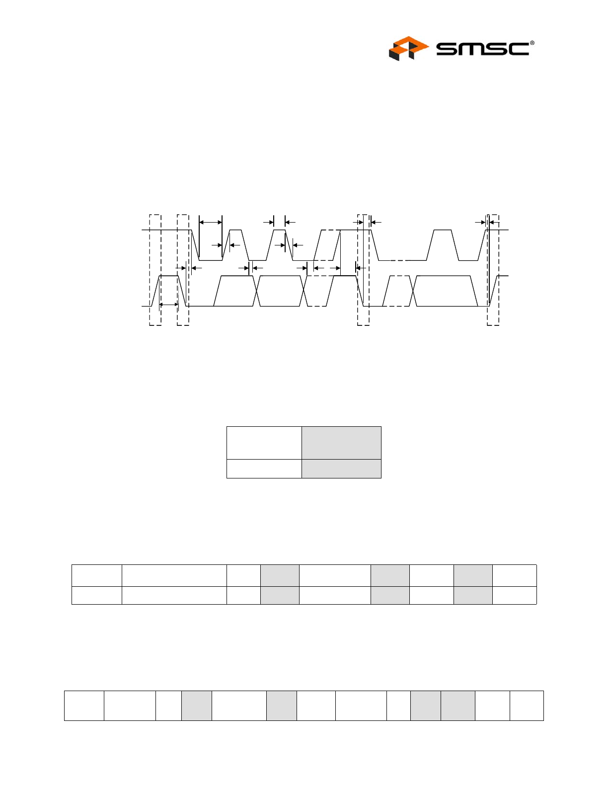
System Management Bus Interface Protocol
A host controller, such as an SMSC I/O controller, communicates with the EMC1043 via the two wire
serial interface named SMBus. The SMBus interface is used to read and write registers in the
EMC1043, which is a slave-only device. A detailed timing diagram is shown in
Figure 2.1
.
Figure 2.1 System Management Bus Timing Diagram
The EMC1043 implements a subset of the SMBus specification and supports Write Byte, Read Byte,
Send Byte, and Receive Byte protocols as shown. In the tables that describe the protocol, the “gray”
columns indicate that the slave is driving the bus.
All of the below protocols use the following convention:
2.3.1
Write Byte
The Write Byte is used to write one byte of data to the registers as shown in
Table 2.3
.
2.3.2
Read Byte
The Read Byte protocol is used to read one byte of data from the registers as shown in
Table 2.4
.
DATA SENT
TO DEVICE
DATA SENT TO
THE HOST
# of bits sent
# of bits sent
Table 2.3 Write Byte Protocol
START
SLAVE ADDRESS
WR
ACK
COMMAND
ACK
DATA
ACK
STOP
1
7
1
1
8
1
8
1
1
Table 2.4 Read Byte Protocol
START
SLAVE
ADDRESS
WR
ACK
COMMAND
ACK
START
SLAVE
ADDRESS
RD
ACK
DATA
NACK
STOP
SMDATA
SMCLK
T
LOW
T
R
T
HIGH
T
F
T
BUF
T
HD:STA
P
S
S - Start Condition
P - Stop Condition
T
HD:DAT
T
SU:DAT
T
SU:STA
T
HD:STA
P
T
SU:STO
S
1°C Triple Temperature Sensor with Beta Compensation and Hotter of Two Zones
Datasheet
Revision 1.44 (04-14-08)
10
SMSC EMC1043
DATASHEET
2.3.3
Send Byte
The Send Byte protocol is used to set the Internal Address Register to the correct Address as shown
in
Table 2.5
. The Send Byte can be followed by the Receive Byte protocol described in
Table 2.6
to
read data from the register. The send byte protocol cannot be used to write data - if data is to be
written to a register then the write byte protocol must be used as described in
Section 2.3.1
.
2.3.4
Receive Byte
The Receive Byte protocol is used to read data from a register when the internal register address
pointer is known to be at the right location (e.g. set via Send Byte). This can be used for consecutive
reads of the same register as shown in
Table 2.6
.
2.3.5
SMBus Timing Diagram
The Timing for the SMBus is shown in
Figure 2.1
.
2.4
SMBus Addresses
The EMC1043 may be ordered with one of four slave addresses as shown in
Ordering Information
.
Attempting to communicate with the EMC1043 SMBus interface with an invalid slave address or invalid
protocol results in no response from the device and does not affect its register contents. The EMC1043
supports stretching of the SMCLK signal by other devices on the SMBus but will not perform this
operation itself.
2.5
SMBus Timeout
The EMC1043 includes an SMBus time-out feature. Following a 25 ms period of inactivity on the
SMBus, the device will time-out and reset the SMBus interface.
1
7
1
1
8
1
1
7
1
1
8
1
1
Table 2.5 Send Byte Protocol
START
SLAVE ADDR
WR
ACK
REG. ADDR
ACK
STOP
1
7
1
1
8
1
1
Table 2.6 Receive Byte Protocol
START
SLAVE ADDR
RD
ACK
REG. DATA
NACK
STOP
1
7
1
1
8
1
1
Table 2.4 Read Byte Protocol
SMSC EMC1043
DATASHEET
Revision 1.44 (04-14-08)
Datasheet
PRODUCT FEATURES
EMC1043
1°C Triple Temperature
Sensor with Beta
Compensation and
Hotter of Two Zones
General Description
The EMC1043 is a family of System Management Bus
(SMBus) temperature sensors that monitors three
temperature zones, one internal diode and two
externally connected diodes, for PC and embedded
e n v i r o n m e n t s . T h e E M C 1 0 4 3 i n c l u d e s b e t a
compensation circuitry to correct for variation in the beta
of measurement transistors. Other extended features
include resistance error correction and ideality factor
configuration to eliminate major sources of temperature
measurement error.
1
An added feature to the EMC1043 is a function that
automatically compares the two external temperature
zones and reports the hotter of the two temperatures.
Selectable conversion rates and standby mode support
low-power operation. The temperature measurement
ranges support two data ranges (and formats), -64°C to
+127°C and -64°C to +191°C.
Applications
Desktop and Notebook Computers
Hardware Management
Servers
Embedded Applications
Features
Supports two External Temperature Diodes
—
±1°C Accuracy (40°C to 80°C)
—
0.125
°C Resolution
—
Ideality Factor Configuration
—
Accepts 2200pF Cap Across External Diodes for Noise
Suppression
—
Optional Resistive Error Correction on External Diode 2
—
Resistance Error Correction (up to 100 Ohms)
—
Beta Compensation
Internal Temperature Diode
—
±3°C Accuracy (0°C to 85°C)
—
0.125
°C Resolution
Low Power Operation
—
4uA Standby Current
3.0V to 3.6V Supply
Programmable Conversion Rate
SMBus 2.0 Compliant
—
Four SMBus Address Available
Reports Hotter of Two Diodes with Dual-core CPU
Simplified Block Diagram
1.Patents pending
Local Temp
Diode
Switching
Current
SMCLK
Internal Diode
Register
Configuration
Register
Status Register
S
M
Bu
s
Inte
rf
ac
e
External Diode
1 Register
External Diode
2 Register
SMDATA
11-bit
delta-sigma
ADC
An
al
og
M
u
x
an
d
A
n
ti
-A
lia
s
F
ilt
er
DP1
DN1
DP2
DN2
Digital Mux
and
Byte Interlock
Reel size is 4,000 pieces.
Evaluation Boards available upon request. (EVB-EMC1043, EVB-EMC1043C)
ORDERING NUMBER
PACKAGE
FEATURES
SMBUS ADDRESS
EMC1043-1-ACZL-TR
8 pinMSOP package
(Lead Free ROHS
compliant)
Two external diodes with
REC and Beta
Compensation and Hottest
Of Comparision
1001_100x
EMC1043-2-ACZL-TR
1001_101x
EMC1043-3-ACZL-TR
1001_000x
EMC1043-4-ACZL-TR
1001_001x
EMC1043-5-ACZL-TR
Two external diodes with
REC. Beta Compensation
on External Diode 1 only.
Hottest of Comparision
1001_100x
1°C Triple Temperature Sensor with Beta Compensation and Hotter of Two Zones
Datasheet
Revision 1.44 (04-14-08)
2
SMSC EMC1043
DATASHEET
80 ARKAY DRIVE, HAUPPAUGE, NY 11788 (631) 435-6000, FAX (631) 273-3123
Copyright © 2008 SMSC or its subsidiaries. All rights reserved.
Circuit diagrams and other information relating to SMSC products are included as a means of illustrating typical applications. Consequently, complete information sufficient for
construction purposes is not necessarily given. Although the information has been checked and is believed to be accurate, no responsibility is assumed for inaccuracies. SMSC
reserves the right to make changes to specifications and product descriptions at any time without notice. Contact your local SMSC sales office to obtain the latest specifications
before placing your product order. The provision of this information does not convey to the purchaser of the described semiconductor devices any licenses under any patent
rights or other intellectual property rights of SMSC or others. All sales are expressly conditional on your agreement to the terms and conditions of the most recently dated
version of SMSC's standard Terms of Sale Agreement dated before the date of your order (the "Terms of Sale Agreement"). The product may contain design defects or errors
known as anomalies which may cause the product's functions to deviate from published specifications. Anomaly sheets are available upon request. SMSC products are not
designed, intended, authorized or warranted for use in any life support or other application where product failure could cause or contribute to personal injury or severe property
damage. Any and all such uses without prior written approval of an Officer of SMSC and further testing and/or modification will be fully at the risk of the customer. Copies of
this document or other SMSC literature, as well as the Terms of Sale Agreement, may be obtained by visiting SMSC’s website at http://www.smsc.com. SMSC is a registered
trademark of Standard Microsystems Corporation (“SMSC”). Product names and company names are the trademarks of their respective holders.
SMSC DISCLAIMS AND EXCLUDES ANY AND ALL WARRANTIES, INCLUDING WITHOUT LIMITATION ANY AND ALL IMPLIED WARRANTIES OF MERCHANTABILITY,
FITNESS FOR A PARTICULAR PURPOSE, TITLE, AND AGAINST INFRINGEMENT AND THE LIKE, AND ANY AND ALL WARRANTIES ARISING FROM ANY COURSE
OF DEALING OR USAGE OF TRADE. IN NO EVENT SHALL SMSC BE LIABLE FOR ANY DIRECT, INCIDENTAL, INDIRECT, SPECIAL, PUNITIVE, OR CONSEQUENTIAL
DAMAGES; OR FOR LOST DATA, PROFITS, SAVINGS OR REVENUES OF ANY KIND; REGARDLESS OF THE FORM OF ACTION, WHETHER BASED ON CONTRACT;
TORT; NEGLIGENCE OF SMSC OR OTHERS; STRICT LIABILITY; BREACH OF WARRANTY; OR OTHERWISE; WHETHER OR NOT ANY REMEDY OF BUYER IS HELD
TO HAVE FAILED OF ITS ESSENTIAL PURPOSE, AND WHETHER OR NOT SMSC HAS BEEN ADVISED OF THE POSSIBILITY OF SUCH DAMAGES.
ORDERING INFORMATION
1°C Triple Temperature Sensor with Beta Compensation and Hotter of Two Zones
Datasheet
SMSC EMC1043
3
Revision 1.44 (04-14-08)
DATASHEET
Table of Contents
Chapter 1
Pin Function . . . . . . . . . . . . . . . . . . . . . . . . . . . . . . . . . . . . . . . . . . . . . . . . . . . . . . . 6
Chapter 2
Electrical Specifications . . . . . . . . . . . . . . . . . . . . . . . . . . . . . . . . . . . . . . . . . . . . . 7
2.1
Absolute Maximum Ratings . . . . . . . . . . . . . . . . . . . . . . . . . . . . . . . . . . . . . . . . . . . . . . . . . . . . . . . 7
2.2
Electrical Specifications . . . . . . . . . . . . . . . . . . . . . . . . . . . . . . . . . . . . . . . . . . . . . . . . . . . . . . . . . . 7
2.3
System Management Bus Interface Protocol . . . . . . . . . . . . . . . . . . . . . . . . . . . . . . . . . . . . . . . . . . 9
2.3.1
Write Byte . . . . . . . . . . . . . . . . . . . . . . . . . . . . . . . . . . . . . . . . . . . . . . . . . . . . . . . . . . . . . 9
2.3.2
Read Byte . . . . . . . . . . . . . . . . . . . . . . . . . . . . . . . . . . . . . . . . . . . . . . . . . . . . . . . . . . . . . 9
2.3.3
Send Byte . . . . . . . . . . . . . . . . . . . . . . . . . . . . . . . . . . . . . . . . . . . . . . . . . . . . . . . . . . . . 10
2.3.4
Receive Byte . . . . . . . . . . . . . . . . . . . . . . . . . . . . . . . . . . . . . . . . . . . . . . . . . . . . . . . . . . 10
2.3.5
SMBus Timing Diagram. . . . . . . . . . . . . . . . . . . . . . . . . . . . . . . . . . . . . . . . . . . . . . . . . . 10
2.4
SMBus Addresses . . . . . . . . . . . . . . . . . . . . . . . . . . . . . . . . . . . . . . . . . . . . . . . . . . . . . . . . . . . . . 10
2.5
SMBus Timeout . . . . . . . . . . . . . . . . . . . . . . . . . . . . . . . . . . . . . . . . . . . . . . . . . . . . . . . . . . . . . . . 10
Chapter 3
Product Description . . . . . . . . . . . . . . . . . . . . . . . . . . . . . . . . . . . . . . . . . . . . . . . . 11
3.1
Power Modes . . . . . . . . . . . . . . . . . . . . . . . . . . . . . . . . . . . . . . . . . . . . . . . . . . . . . . . . . . . . . . . . . 11
3.2
One Shot During Standby Mode. . . . . . . . . . . . . . . . . . . . . . . . . . . . . . . . . . . . . . . . . . . . . . . . . . . 11
3.3
Operation During Run Mode. . . . . . . . . . . . . . . . . . . . . . . . . . . . . . . . . . . . . . . . . . . . . . . . . . . . . . 12
3.3.1
Conversion Rates . . . . . . . . . . . . . . . . . . . . . . . . . . . . . . . . . . . . . . . . . . . . . . . . . . . . . . 12
3.3.2
Dynamic Averaging . . . . . . . . . . . . . . . . . . . . . . . . . . . . . . . . . . . . . . . . . . . . . . . . . . . . . 12
3.4
Temperature Monitors . . . . . . . . . . . . . . . . . . . . . . . . . . . . . . . . . . . . . . . . . . . . . . . . . . . . . . . . . . 13
3.5
Temperature Measurement Results and Data . . . . . . . . . . . . . . . . . . . . . . . . . . . . . . . . . . . . . . . . 14
3.6
Resistance Error Correction (REC) . . . . . . . . . . . . . . . . . . . . . . . . . . . . . . . . . . . . . . . . . . . . . . . . 15
3.7
Beta Compensation . . . . . . . . . . . . . . . . . . . . . . . . . . . . . . . . . . . . . . . . . . . . . . . . . . . . . . . . . . . . 15
3.8
Programmable Ideality Factor. . . . . . . . . . . . . . . . . . . . . . . . . . . . . . . . . . . . . . . . . . . . . . . . . . . . . 16
3.9
Diode Faults . . . . . . . . . . . . . . . . . . . . . . . . . . . . . . . . . . . . . . . . . . . . . . . . . . . . . . . . . . . . . . . . . . 16
Chapter 4
Register Set and Description. . . . . . . . . . . . . . . . . . . . . . . . . . . . . . . . . . . . . . . . . 17
4.1
Legacy Temperature Data Registers (00h, 23h, 01h, 10h, F8h, F9h) . . . . . . . . . . . . . . . . . . . . . . 19
4.2
Extended Format Temperature Registers (FAh-FDh) . . . . . . . . . . . . . . . . . . . . . . . . . . . . . . . . . . 19
4.3
Status Register - 02h . . . . . . . . . . . . . . . . . . . . . . . . . . . . . . . . . . . . . . . . . . . . . . . . . . . . . . . . . . . 20
4.4
Configuration Register (03h Read, 09h Write) . . . . . . . . . . . . . . . . . . . . . . . . . . . . . . . . . . . . . . . . 20
4.5
Configuration 2 Register - (04h) . . . . . . . . . . . . . . . . . . . . . . . . . . . . . . . . . . . . . . . . . . . . . . . . . . . 21
4.6
One Shot Register - (0Fh) . . . . . . . . . . . . . . . . . . . . . . . . . . . . . . . . . . . . . . . . . . . . . . . . . . . . . . . 22
4.7
Ideality Configuration Registers (27h - 28h) . . . . . . . . . . . . . . . . . . . . . . . . . . . . . . . . . . . . . . . . . . 22
4.8
Beta Configuration Registers (29h - 2Ah). . . . . . . . . . . . . . . . . . . . . . . . . . . . . . . . . . . . . . . . . . . . 24
4.9
Product ID Register (EDh) . . . . . . . . . . . . . . . . . . . . . . . . . . . . . . . . . . . . . . . . . . . . . . . . . . . . . . . 25
4.10
Manufacturer ID Register (FEh) . . . . . . . . . . . . . . . . . . . . . . . . . . . . . . . . . . . . . . . . . . . . . . . . . . . 25
4.11
Revision Register (FFh) . . . . . . . . . . . . . . . . . . . . . . . . . . . . . . . . . . . . . . . . . . . . . . . . . . . . . . . . . 25
Chapter 5
Typical Operating Curves. . . . . . . . . . . . . . . . . . . . . . . . . . . . . . . . . . . . . . . . . . . 26
Chapter 6
Package Outline . . . . . . . . . . . . . . . . . . . . . . . . . . . . . . . . . . . . . . . . . . . . . . . . . . . 28
6.1
Package Markings . . . . . . . . . . . . . . . . . . . . . . . . . . . . . . . . . . . . . . . . . . . . . . . . . . . . . . . . . . . . . 29
1°C Triple Temperature Sensor with Beta Compensation and Hotter of Two Zones
Datasheet
Revision 1.44 (04-14-08)
4
SMSC EMC1043
DATASHEET
List of Figures
Figure 1.1 EMC1043 Pin Diagram . . . . . . . . . . . . . . . . . . . . . . . . . . . . . . . . . . . . . . . . . . . . . . . . . . . . . . 6
Figure 2.1 System Management Bus Timing Diagram . . . . . . . . . . . . . . . . . . . . . . . . . . . . . . . . . . . . . . . 9
Figure 3.1 EMC1043 System Drawing . . . . . . . . . . . . . . . . . . . . . . . . . . . . . . . . . . . . . . . . . . . . . . . . . . 11
Figure 3.2 Block Diagram of Temperature Monitoring Circuit . . . . . . . . . . . . . . . . . . . . . . . . . . . . . . . . . 13
Figure 3.3 External Diode Configurations . . . . . . . . . . . . . . . . . . . . . . . . . . . . . . . . . . . . . . . . . . . . . . . . 14
Figure 6.1 8-Pin MSOP Package Outline - 3x3mm Body 0.65mm Pitch. . . . . . . . . . . . . . . . . . . . . . . . . 28
1°C Triple Temperature Sensor with Beta Compensation and Hotter of Two Zones
Datasheet
SMSC EMC1043
5
Revision 1.44 (04-14-08)
DATASHEET
List of Tables
Table 1.1 EMC1043 Pin Description . . . . . . . . . . . . . . . . . . . . . . . . . . . . . . . . . . . . . . . . . . . . . . . . . . . . . 6
Table 2.1 Absolute Maximum Ratings . . . . . . . . . . . . . . . . . . . . . . . . . . . . . . . . . . . . . . . . . . . . . . . . . . . . 7
Table 2.2 Electrical Characteristics . . . . . . . . . . . . . . . . . . . . . . . . . . . . . . . . . . . . . . . . . . . . . . . . . . . . . . 7
Table 2.3 Write Byte Protocol . . . . . . . . . . . . . . . . . . . . . . . . . . . . . . . . . . . . . . . . . . . . . . . . . . . . . . . . . . 9
Table 2.4 Read Byte Protocol . . . . . . . . . . . . . . . . . . . . . . . . . . . . . . . . . . . . . . . . . . . . . . . . . . . . . . . . . . 9
Table 2.5 Send Byte Protocol . . . . . . . . . . . . . . . . . . . . . . . . . . . . . . . . . . . . . . . . . . . . . . . . . . . . . . . . . 10
Table 2.6 Receive Byte Protocol . . . . . . . . . . . . . . . . . . . . . . . . . . . . . . . . . . . . . . . . . . . . . . . . . . . . . . . 10
Table 3.1 Supply Current vs. Conversion Rate and ADC Averaging Factor . . . . . . . . . . . . . . . . . . . . . . 12
Table 3.2 EMC1043 Temperature Data Format . . . . . . . . . . . . . . . . . . . . . . . . . . . . . . . . . . . . . . . . . . . 15
Table 4.1 EMC1043 Register Set . . . . . . . . . . . . . . . . . . . . . . . . . . . . . . . . . . . . . . . . . . . . . . . . . . . . . . 17
Table 4.2 Status Register . . . . . . . . . . . . . . . . . . . . . . . . . . . . . . . . . . . . . . . . . . . . . . . . . . . . . . . . . . . . 20
Table 4.3 Configuration Register . . . . . . . . . . . . . . . . . . . . . . . . . . . . . . . . . . . . . . . . . . . . . . . . . . . . . . . 20
Table 4.4 Conversion Rate . . . . . . . . . . . . . . . . . . . . . . . . . . . . . . . . . . . . . . . . . . . . . . . . . . . . . . . . . . . 21
Table 4.5 Configuration 2 Register . . . . . . . . . . . . . . . . . . . . . . . . . . . . . . . . . . . . . . . . . . . . . . . . . . . . . 21
Table 4.6 One Shot Registers . . . . . . . . . . . . . . . . . . . . . . . . . . . . . . . . . . . . . . . . . . . . . . . . . . . . . . . . . 22
Table 4.7 Ideality Configuration Registers. . . . . . . . . . . . . . . . . . . . . . . . . . . . . . . . . . . . . . . . . . . . . . . . 22
Table 4.8 Ideality Factor Look Up Table . . . . . . . . . . . . . . . . . . . . . . . . . . . . . . . . . . . . . . . . . . . . . . . . . 23
Table 4.9 Substrate Diode Ideality Factor Look-Up Table (BJT Model) . . . . . . . . . . . . . . . . . . . . . . . . . 23
Table 4.10 Beta Configuration Registers. . . . . . . . . . . . . . . . . . . . . . . . . . . . . . . . . . . . . . . . . . . . . . . . . . 24
Table 4.11 Beta Configuration Look Up Table. . . . . . . . . . . . . . . . . . . . . . . . . . . . . . . . . . . . . . . . . . . . . . 24
Table 4.12 Product ID Register . . . . . . . . . . . . . . . . . . . . . . . . . . . . . . . . . . . . . . . . . . . . . . . . . . . . . . . . . 25
Table 4.13 Manufacturer ID Register. . . . . . . . . . . . . . . . . . . . . . . . . . . . . . . . . . . . . . . . . . . . . . . . . . . . . 25
Table 4.14 Revision Register. . . . . . . . . . . . . . . . . . . . . . . . . . . . . . . . . . . . . . . . . . . . . . . . . . . . . . . . . . . 25
Table 6.1 8-Pin MSOP Package Parameters . . . . . . . . . . . . . . . . . . . . . . . . . . . . . . . . . . . . . . . . . . . . . 28
1°C Triple Temperature Sensor with Beta Compensation and Hotter of Two Zones
Datasheet
Revision 1.44 (04-14-08)
6
SMSC EMC1043
DATASHEET
Chapter 1 Pin Function
Figure 1.1 EMC1043 Pin Diagram
Table 1.1 EMC1043 Pin Description
PIN
PIN NO.
DESCRIPTION
DP1
1
External Diode 1 Positive (anode) Connection
DN1
2
External Diode 1 Negative (cathode) Connection
DP2
3
External Diode 2 Positive (anode) Connection
DN2
4
External Diode 2 Negative (cathode) Connection
GND
5
Ground
VDD
6
Supply Voltage
SMDATA
7
System Management Bus Data - bi-directional data, open drain output
SMCLK
8
System Management Bus Clock Input
8-MSOP
8
7
6
5
1
2
3
4
DP1
DN1
DP2
DN2
SMCLK
SMDATA
VDD
GND
1°C Triple Temperature Sensor with Beta Compensation and Hotter of Two Zones
Datasheet
SMSC EMC1043
7
Revision 1.44 (04-14-08)
DATASHEET
Chapter 2 Electrical Specifications
2.1
Absolute Maximum Ratings
Note: Stresses above those listed could cause damage to the device. This is a stress rating only and
functional operation of the device at any other condition above those indicated in the operation
sections of this specification is not implied. When powering this device from laboratory or
system power supplies, it is important that the Absolute Maximum Ratings not be exceeded or
device failure can result. Some power supplies exhibit voltage spikes on their outputs when the
AC power is switched on or off. In addition, voltage transients on the AC power line may appear
on the DC output. If this possibility exists, it is suggested that a clamp circuit be used.
2.2
Electrical Specifications
Table 2.1 Absolute Maximum Ratings
DESCRIPTION
RATING
UNIT
Supply Voltage V
DD
-0.3 to 5.0
V
Voltage on SMDATA and SMCLK
pins
-0.3 to 5.5
V
Voltage on any other pin
-0.3 to VDD+0.3
V
Operating Temperature Range
-40 to 125
°C
Storage Temperature Range
-55 to 150
°C
Lead Temperature Range
Refer to JEDEC
Spec. J-STD-020
Package Thermal Characteristics for MSOP-8
Thermal Resistance T
JA
(at 0 air flow)
135.9
°C/W
ESD Rating, All Pins Human Body Model
2000
V
Table 2.2 Electrical Characteristics
V
DD
=3.0V to 3.6V, T
A
= -20
°C to +85°C, Typical values at T
A
= 27
°C unless otherwise noted
PARAMETER
SYMBOL
MIN
TYP
MAX
UNITS
CONDITIONS
DC Power
Supply Voltage
V
DD
3.0
3.3
3.6
V
Average Operating Current
I
DD
340
400
μA
4 conversions/s
See
Table 4.4
.
I
STBY
2
4
μA
Standby mode
Internal Temperature Monitor
Temperature Accuracy
± 1
± 3
°C
-20
°C≤ T
A
≤85°C
± 1.5
°C
0
°C < T
A
≤ 85°C
Temperature Resolution
0.125
°C
1°C Triple Temperature Sensor with Beta Compensation and Hotter of Two Zones
Datasheet
Revision 1.44 (04-14-08)
8
SMSC EMC1043
DATASHEET
External Temperature Monitor
Temperature Accuracy
Remote Diode 40
°C to 80°C
Remote Diode -20
°C to 125°C
Remote Diode -64
°C to 192°C
± 1
± 3
± 5
°C
°C
°C
15
°C≤T
A
≤70°C
-20
°C≤T
A
≤85°C
-20
°C≤T
A
≤85°C
Temperature Resolution
0.125
°C
Filter Capacitor
C
FILTER
2.2
nF
Connected across
external diode
Note 2.2
Voltage Tolerance
Voltage at pin (
SMDATA,SMCLK)
V
TOL
-0.3
5.5
V
SMBus Interface (SMDATA,SMCLK)
Input High Level
V
IH
2.0
V
Input Low Level
V
IL
0.8
V
Input High/Low Current
I
IH
/I
IL
-1
1
μ
A
Hysteresis
500
mV
Input Capacitance
5
pF
Output Low Sink Current
6
mA
SMDATA = 0.6V
SMBus Timing
Clock Frequency
F
SMB
10
400
kHz
Spike Suppression
50
ns
Bus free time Start to Stop
T
BUF
1.3
μ
s
Hold time Start
T
HD:STA
0.6
μ
s
Setup time Start
T
SU:STA
0.6
μ
s
Setup time Stop
T
SU:STO
0.6
μ
s
Data Hold Time
T
HD:DAT
0.3
μ
s
Data Setup Time
T
SU:DAT
100
ns
Clock Low Period
T
LOW
1.3
μ
s
Clock High Period
T
HIGH
0.6
μ
s
Clock/Data Fall Time
T
F
*
300
ns
*Min = 20+0.1C
b
ns
Clock/Data Rise Time
T
R
*
300
Note
2.1
ns
*Min = 20+0.1C
b
ns
Capacitive Load (each bus line)
C
b
0.6
400
pF
Table 2.2 Electrical Characteristics (continued)
V
DD
=3.0V to 3.6V, T
A
= -20
°C to +85°C, Typical values at T
A
= 27
°C unless otherwise noted
PARAMETER
SYMBOL
MIN
TYP
MAX
UNITS
CONDITIONS
1°C Triple Temperature Sensor with Beta Compensation and Hotter of Two Zones
Datasheet
SMSC EMC1043
9
Revision 1.44 (04-14-08)
DATASHEET
Note 2.1
300nS rise time max is required for 400kHz bus operation. For lower clock frequencies,
the maximum rise time is (0.1/F
SMB
)+50nS
Note 2.2
See SMSC Applications for Application Notes and Guidelines when measuring GPU
processor diodes and CPU processor diodes.
2.3
System Management Bus Interface Protocol
A host controller, such as an SMSC I/O controller, communicates with the EMC1043 via the two wire
serial interface named SMBus. The SMBus interface is used to read and write registers in the
EMC1043, which is a slave-only device. A detailed timing diagram is shown in
Figure 2.1
.
Figure 2.1 System Management Bus Timing Diagram
The EMC1043 implements a subset of the SMBus specification and supports Write Byte, Read Byte,
Send Byte, and Receive Byte protocols as shown. In the tables that describe the protocol, the “gray”
columns indicate that the slave is driving the bus.
All of the below protocols use the following convention:
2.3.1
Write Byte
The Write Byte is used to write one byte of data to the registers as shown in
Table 2.3
.
2.3.2
Read Byte
The Read Byte protocol is used to read one byte of data from the registers as shown in
Table 2.4
.
DATA SENT
TO DEVICE
DATA SENT TO
THE HOST
# of bits sent
# of bits sent
Table 2.3 Write Byte Protocol
START
SLAVE ADDRESS
WR
ACK
COMMAND
ACK
DATA
ACK
STOP
1
7
1
1
8
1
8
1
1
Table 2.4 Read Byte Protocol
START
SLAVE
ADDRESS
WR
ACK
COMMAND
ACK
START
SLAVE
ADDRESS
RD
ACK
DATA
NACK
STOP
SMDATA
SMCLK
T
LOW
T
R
T
HIGH
T
F
T
BUF
T
HD:STA
P
S
S - Start Condition
P - Stop Condition
T
HD:DAT
T
SU:DAT
T
SU:STA
T
HD:STA
P
T
SU:STO
S
1°C Triple Temperature Sensor with Beta Compensation and Hotter of Two Zones
Datasheet
Revision 1.44 (04-14-08)
10
SMSC EMC1043
DATASHEET
2.3.3
Send Byte
The Send Byte protocol is used to set the Internal Address Register to the correct Address as shown
in
Table 2.5
. The Send Byte can be followed by the Receive Byte protocol described in
Table 2.6
to
read data from the register. The send byte protocol cannot be used to write data - if data is to be
written to a register then the write byte protocol must be used as described in
Section 2.3.1
.
2.3.4
Receive Byte
The Receive Byte protocol is used to read data from a register when the internal register address
pointer is known to be at the right location (e.g. set via Send Byte). This can be used for consecutive
reads of the same register as shown in
Table 2.6
.
2.3.5
SMBus Timing Diagram
The Timing for the SMBus is shown in
Figure 2.1
.
2.4
SMBus Addresses
The EMC1043 may be ordered with one of four slave addresses as shown in
Ordering Information
.
Attempting to communicate with the EMC1043 SMBus interface with an invalid slave address or invalid
protocol results in no response from the device and does not affect its register contents. The EMC1043
supports stretching of the SMCLK signal by other devices on the SMBus but will not perform this
operation itself.
2.5
SMBus Timeout
The EMC1043 includes an SMBus time-out feature. Following a 25 ms period of inactivity on the
SMBus, the device will time-out and reset the SMBus interface.
1
7
1
1
8
1
1
7
1
1
8
1
1
Table 2.5 Send Byte Protocol
START
SLAVE ADDR
WR
ACK
REG. ADDR
ACK
STOP
1
7
1
1
8
1
1
Table 2.6 Receive Byte Protocol
START
SLAVE ADDR
RD
ACK
REG. DATA
NACK
STOP
1
7
1
1
8
1
1
Table 2.4 Read Byte Protocol