

2015 Microchip Technology Inc.
DS20005411A-page 1
EMC1001
Features
• Self-Contained Internal Temperature Sensor
- +0.25°C resolution
- ±1.5°C Accuracy +40°C to +85°C
• SMBus Address Selected by External Resistor:
- Select 1 of 4 per package, 8 addresses
available
• Maskable Interrupt using ALERT pin
• One-shot Command during Standby
• Low Power, 3.0V to 3.6V Supply
• 47 µA at 0.0625 Conversions per Second
(Typical)
• 4.8 µA in Standby (Typical)
• SMBus 2.0 Compliant interface
• Programmable Temperature Conversion Rate
• Small 6-lead TSOT package
Applications
• Desktop and Notebook Computers
• Thermostats
• Smart batteries
• Industrial/Automotive
• Other Electronic Systems
General Description
The EMC1001 is a tiny SMBus temperature sensor
with ±1.5°C accuracy and two interrupts. Packaged in
a SOT23-6, the EMC1001 provides an accurate,
low-cost, low-current solution for critical temperature
monitoring in a PC or in embedded applications.
The EMC1001 generates two separate interrupts with
programmable thermal trip points. The THERM output
operates as a thermostat with programmable threshold
and hysteresis. The ALERT output can be configured
as a maskable SMBus alert with programmable win-
dow comparator limits, or as a second THERM output.
An efficient fan control system can be created since
this output may be used to control a fan.
A power-down mode extends battery life in portable
applications.
Each part number may be configured to respond to one
of four separate SMBus addresses.
Package Types
4
1
2
3
6 SMDATA
SMCLK
ADDR/THERM
GND
V
DD
5 ALERT/THERM2
EMC1001
6-Lead TSOT
±1.5°C SMBus Temperature Sensor in Miniature TSOT
EMC1001
DS2
0005411A-p
age 2
20
15 M
ic
rochip
T
e
c
hnology
In
c
.
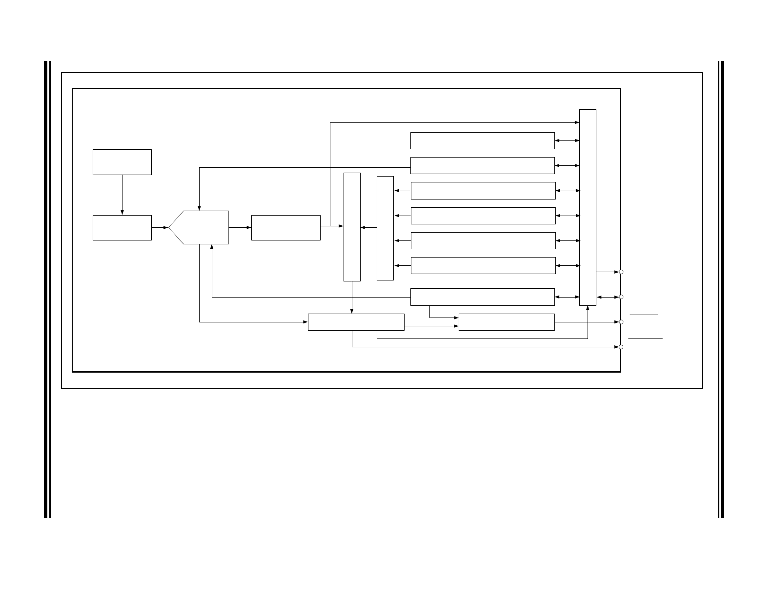
Simplified Block Diagram
EMC1001
Internal
Temp Diode
Switching
Current
SMCLK
Digital Mux
Limit
Co
mp
arat
or
High Limit Registers
THERM Hysteresis Register
Low Limit Registers
THERM Limit Register
Address Pointer Register
Conversion Rate Register
Interrupt Masking
Status Register
Configuration Register
SMBus Interface
Temperature
Register
ALERT
SMDATA
10-bit
delta-sigma
ADC
THERM
2015 Microchip Technology Inc.
DS20005411A-page 3
EMC1001
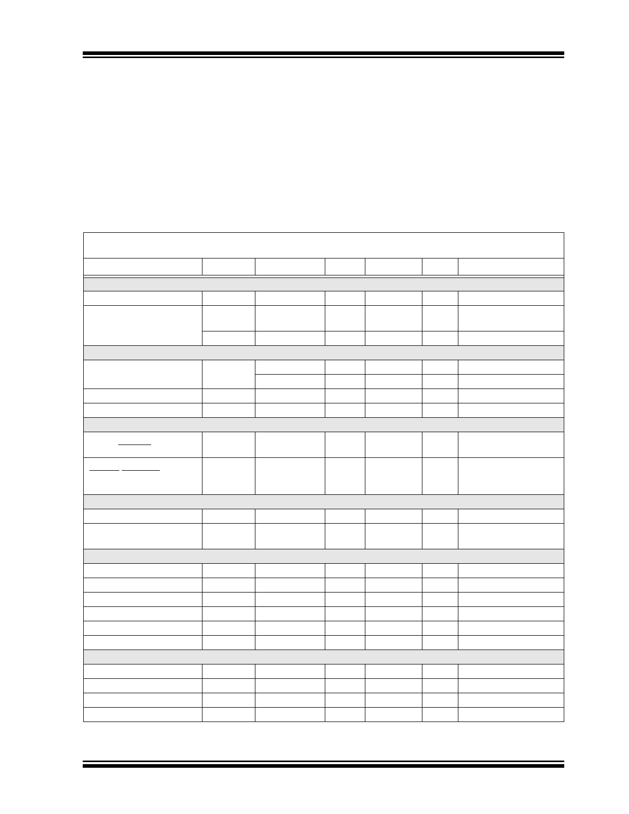
1.0
ELECTRICAL
CHARACTERISTICS
Absolute Maximum Ratings†
Supply Voltage VDD..............................................-0.3 to 5.0V
Voltage on ALERT/THERM2, SMDATA and SMCLK pins ......
..............................................................................-0.3 to 5.5V
Voltage on any other pin .............................. -0.3 to V
DD
+0.3V
Lead Temperature Range .......................................................
.......................................... Refer to JEDEC Spec. J-STD-020
ESD Rating, All Pins (Human Body Model) ..................2000V
† Notice: Stresses above those listed under “Maximum
Ratings” may cause permanent damage to the device.
This is a stress rating only and functional operation of
the device at those or any other conditions above those
indicated in the operational sections of this
specification is not intended. Exposure to maximum
rating conditions for extended periods may affect
device reliability.
ELECTRICAL SPECIFICATIONS
Electrical Characteristics: Unless otherwise noted, V
DD
= 3.0V to 3.6V, T
A
= -25°C to +125°C,
Typical values at T
A
= +27°C.
Parameter
Symbol
Min.
Typ.
Max.
Units
Conditions
DC Power
Supply Voltage
V
DD
3.0
3.3
3.6
V
Average Operating Current
I
DD
—
36
—
mA
0.0625 conversion/s,
see
Table 4-4
I
PD
—
4.8
10
µA
Standby mode
Temperature Measurement
Accuracy
—
±0.5
±1.5
°C
+40°C
T
A
85°C
—
±1
±3
°C
-25°C
T
A
125°C
Resolution
—
0.25
—
°C
Conversion Time
—
26
—
ms
Voltage Tolerance
Voltage at pin
(ADDR/THERM)
V
TOL
-0.3
—
3.6
V
Voltage at pin
(ALERT/THERM2,
SMDATA,SMCLK)
V
TOL
-0.3
—
5.5
V
Digital Outputs (ADDR/THERM, ALERT/THERM2)
Output Low Voltage
V
OL
—
—
0.4
V
I
OUT
= -4 mA
High Level
Leakage Current
I
OH
—
0.1
1
mA
V
OUT
= V
DD
SMBus Interface (SMDATA,SMCLK)
Input High Level
V
IH
2.0
—
—
V
Input Low Level
V
IL
—
0.8
V
Input High/Low Current
I
IH
/I
IL
-1
—
1
mA
Hysteresis
—
500
—
mV
Input Capacitance
—
5
—
pF
Output Low Sink Current
6
—
mA
SMDATA = 0.6V
SMBus Timing
Clock Frequency
F
SMB
10
—
400
kHz
Spike Suppression
—
—
50
ns
Bus Free Time Start to Stop
T
BUF
1.3
—
—
µs
Hold Time Start
THD:STA
0.6
—
—
µs
Note 1:
300 ns rise time maximum is required for 400 kHz bus operation. For lower clock frequencies, the
maximum rise time is (0.1/F
SMB
) + 50 ns.
EMC1001
DS20005411A-page 4
2015 Microchip Technology Inc.
Setup Time Start
TSU:STA
0.6
—
—
µs
Setup Time Stop
TSU:STO
0.6
—
—
µs
Data Hold Time
THD:DAT
0.3
—
—
µs
Data Setup Time
TSU:DAT
100
—
—
ns
Clock Low Period
T
LOW
1.3
—
—
µs
Clock High Period
T
HIGH
0.6
—
—
µs
Clock/Data Fall Time
T
F
20 + 0.1C
b
—
300
ns
Clock/Data Rise Time
T
R
20 + 0.1C
b
—
300
(
1
)
ns
Capacitive Load (each bus
line)
Cb
0.6
—
400
pF
TABLE 1-1:
SMBUS ADDRESS CONFIGURATION INFORMATION
Part Number
ADDR/THERM Pull-up Resistor
SMBus Address
Package Description
EMC1001
7.5 k
±5%
(
Note 1
,
Note 2
)
100 1000b
6-Lead TSOT
12 k
±5% (
Note 2
)
100 1001b
6-Lead TSOT
20 k
±5% (
Note 2
)
011 1000b
6-Lead TSOT
33 k
±5% (
Note 2
)
011 1001b
6-Lead TSOT
EMC1001-1
7.5 k
±5% (
Note 1
,
Note 2
)
100 1010b
6-Lead TSOT
12 k
±5% (
Note 2
)
100 1011b
6-Lead TSOT
20 k
±5% (
Note 2
)
011 1010b
6-Lead TSOT
33 k
±5% (
Note 2
)
011 1011b
6-Lead TSOT
Note 1:
This value must be greater than 1 k
5% and less than or equal to 7.5 k5%
2:
The pull-up resistor must be connected to V
DD
(pin 1), and the total capacitance on this pin must be less
than 100 pF.
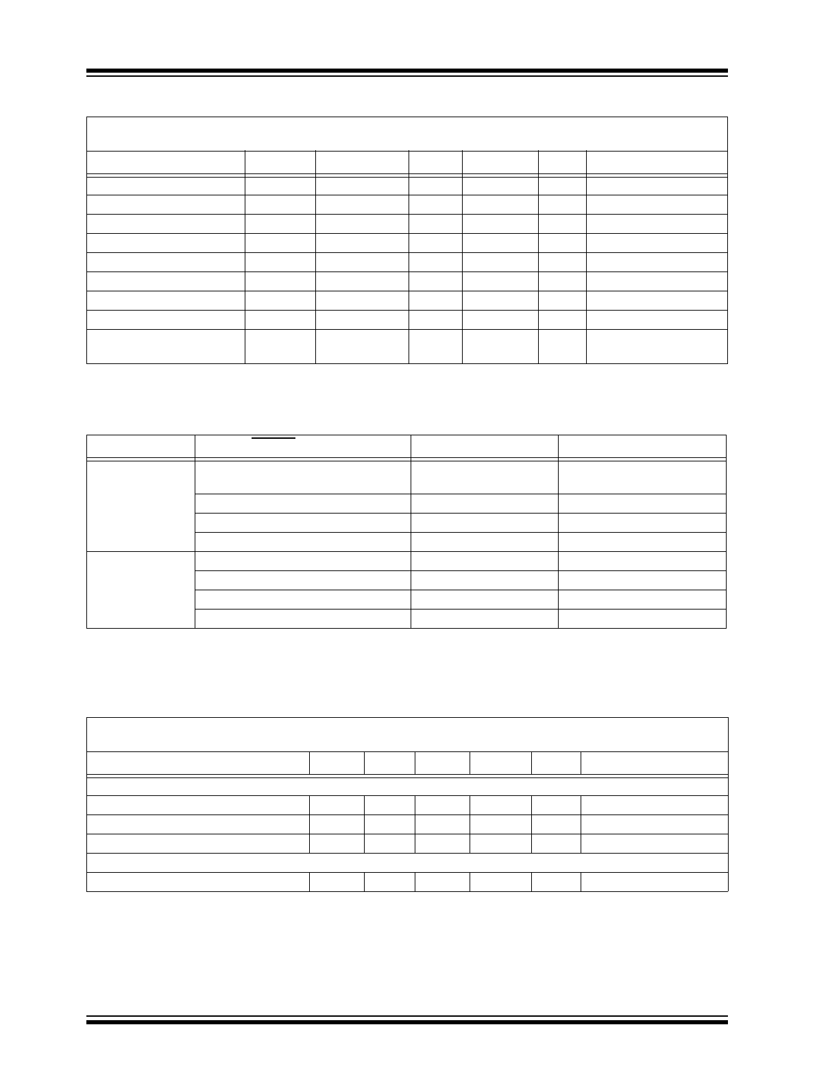
ELECTRICAL SPECIFICATIONS (CONTINUED)
Electrical Characteristics: Unless otherwise noted, V
DD
= 3.0V to 3.6V, T
A
= -25°C to +125°C,
Typical values at T
A
= +27°C.
Parameter
Symbol
Min.
Typ.
Max.
Units
Conditions
Note 1:
300 ns rise time maximum is required for 400 kHz bus operation. For lower clock frequencies, the
maximum rise time is (0.1/F
SMB
) + 50 ns.
TEMPERATURE SPECIFICATIONS
Electrical Characteristics: Unless otherwise noted, V
DD
= 3.0V to 3.6V, T
A
= -25°C to +125°C,
Typical values at T
A
= +27°C.
Parameters
Sym.
Min.
Typ.
Max.
Units
Conditions
Temperature Ranges
Operating Ambient Temperature Range
T
A
-25
—
+125
°C
Storage Temperature Range
T
A
-55
—
+150
°C
Maximum Junction Temperature
T
J
-40
—
+150
°C
Package Thermal Resistances
Thermal Resistance, 6L-TSOT
JA
—
112
—
°C/W
2015 Microchip Technology Inc.
DS20005411A-page 5
EMC1001
2.0
PIN DESCRIPTION
The descriptions of the pins are listed in
Table 2-1
.
TABLE 2-1:
PIN FUNCTION TABLE
TSOT
Pin Number
Description
1
ADDR/THERM
Logic output pin that can be used to turn on/off a fan or throttle a CPU clock
in the event of an overtemperature condition. This is an open-drain output.
This pin is sampled following power-up and the value of the pull-up resistor
determines the SMBus slave address (see
Table 1-1
). Total capacitance on
this pin must not exceed 100 pF, and the pull-up resistor must be connected
to the same supply voltage as V
DD
.
2
GND
Ground pin
3
V
DD
Supply Voltage pin, 3.0V to 3.6V
4
SMCLK
SMBus Clock Input pin
5
ALERT/THERM2
Logic Output pin used as interrupt, SMBus alert or as a second THERM
output. This is an open-drain output.
6
SMDATA
SMBus Data Input/Output pin, open-drain output
EMC1001
DS20005411A-page 6
2015 Microchip Technology Inc.
3.0
SYSTEM MANAGEMENT BUS
INTERFACE PROTOCOL
A host controller, such as an I/O controller,
communicates with the EMC1001 via the two-wire
serial interface named SMBus. The SMBus interface is
used to read and write registers in the EMC1001, which
is a slave-only device. A detailed timing diagram is
shown in
Figure 3-1
.
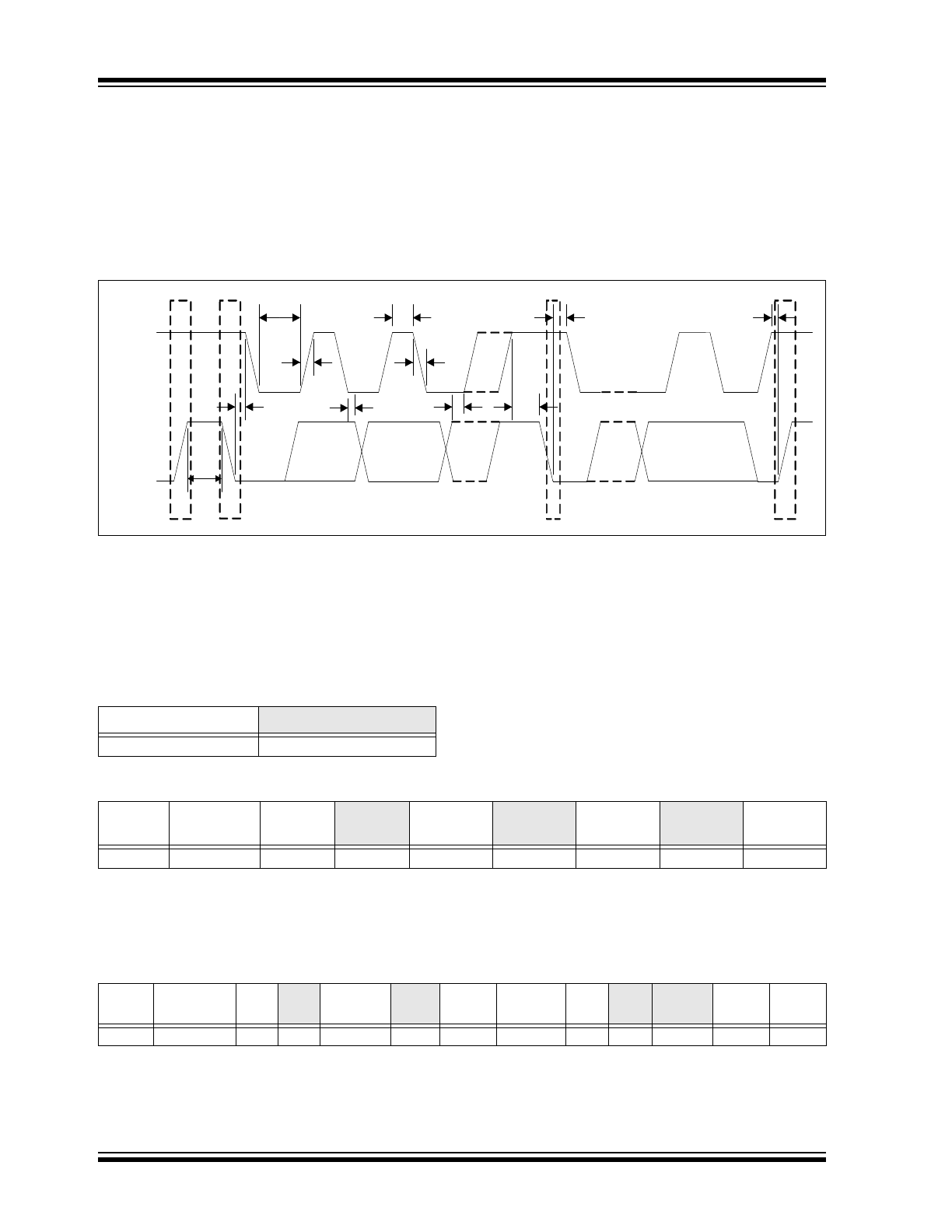
FIGURE 3-1:
System Management Bus Timing Diagram.
The EMC1001 implements a subset of the SMBus
specification and supports Write Byte, Read Byte,
Send Byte, Receive Byte and Alert Response Address
protocols, as shown in the following sections.
All protocols in these sections use the convention in
Table 3-1
.
3.1
SMBus Write Byte
The Write Byte is used to write one byte of data to a
specific register as shown in
Table 3-2
.
3.2
SMBus Read Byte
The Read Byte protocol is used to read one byte of data
from the registers as shown in
Table 3-3
.
SMDATA
SMCLK
T
BUF
P
S
S - Start Condition
P - Stop Condition
P
S
T
HIGH
T
LOW
T
HD:STA
T
SU:STO
T
HD:STA
T
HD:DAT
T
SU:DAT
T
SU:STA
T
FALL
T
RISE
TABLE 3-1:
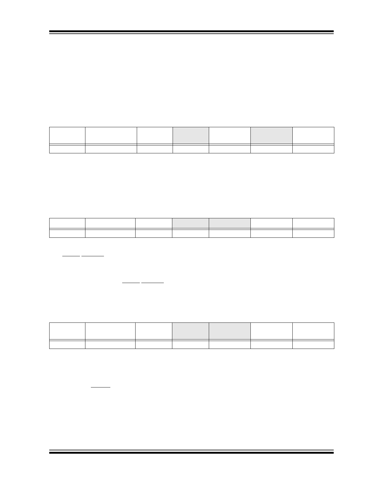
PROTOCOL FORMAT
Data Sent to Device
Data Sent to the Host
Data sent
Data sent
TABLE 3-2:
WRITE BYTE PROTOCOL
START
Slave
Address
WR
ACK
Command
ACK
Data
ACK
STOP
1
7
1
1
8
1
8
1
1
TABLE 3-3:
READ BYTE PROTOCOL
START
Slave
Address
WR
ACK
Command
ACK
START
Slave
Address
RD
ACK
Data
NACK
STOP
1
7
1
1
8
1
1
7
1
1
8
1
1
2015 Microchip Technology Inc.
DS20005411A-page 7
EMC1001
3.3
SMBus Send Byte
The Send Byte protocol is used to set the Internal
Address Register to the correct Address. The Send
Byte can be followed by the Receive Byte protocol
(
Section 3.4 “SMBus Receive Byte”
) in order to read
data from the register. The send byte protocol cannot
be used to write data; if data is to be written to a regis-
ter, then the Write Byte protocol must be used (see
Section 3.1 “SMBus Write Byte”
). The Send Byte
protocol is shown in
Table 3-4
.
3.4
SMBus Receive Byte
The Receive Byte protocol is used to read data from a
register when the internal register address pointer is
known to be at the right location (e.g., set via Send
Byte). This is used for consecutive reads of the same
register as shown in
Table 3-5
.
3.5
Alert Response Address
The ALERT/THERM2 output can be used as an
SMBALERT# as described in
Section 4.3
“ALERT/THERM2 Output”
The Alert Response
Address is polled by the Host whenever it detects an
SMBALERT#, i.e. when the ALERT/THERM2 pin is
asserted. The EMC1001 will acknowledge the Alert
Response Address and respond with its device
address as shown in
Table 3-6
.
3.6
SMBus Addresses
The EMC1001 is available in two versions (EMC1001
and EMC1001-1), each of which has four 7-bit slave
addresses that are enabled based on the pull-up resis-
tor on the ADDR/THERM pin. The value of this pull-up
resistor determines the slave address per
Table 1-1
.
Attempting to communicate with the EMC1001 SMBus
interface with an invalid slave address or invalid proto-
col results in no response from the device and does not
affect its register contents.
The EMC1001 supports stretching of the SMCLK
signal by other devices on the SMBus but will not
perform this operation itself. The EMC1001 has an
SMBus timeout feature. Bit 7 of the SMBus Timeout
Enable register enables this function when set to 1 (the
default setting is 0). When this feature is enabled, the
SMBus will timeout after approximately 25 ms of
inactivity.
TABLE 3-4:
SEND BYTE PROTOCOL
START
Slave Address
WR
ACK
Register
Address
ACK
STOP
1
7
1
1
8
1
1
TABLE 3-5:
RECEIVE BYTE PROTOCOL
START
Slave Address
RD
ACK
Register Data
NACK
STOP
1
7
1
1
8
1
1
TABLE 3-6:
MODIFIED SMBUS RECEIVE BYTE PROTOCOL RESPONSE TO ARA
START
Alert Response
Address
RD
ACK
EMC1001
Slave Address
NACK
STOP
1
7
1
1
8
1
1
EMC1001
DS20005411A-page 8
2015 Microchip Technology Inc.
4.0
PRODUCT DESCRIPTION
The EMC1001 is an SMBus temperature sensor that
monitors a single temperature zone. Thermal manage-
ment is performed in cooperation with a host device.
The host reads the temperature data from the
EMC1001 and takes appropriate action such as con-
trolling fan speed or processor clock frequency. The
EMC1001 has programmable temperature-limit regis-
ters that define a safe operating window. After the host
has configured the temperature limits, the EMC1001
can operate as a free-running independent watchdog
to warn the host of temperature hot-spots, without
requiring the host to poll the device. The
ADDR/THERM output can be used to control a fan
without host intervention.
FIGURE 4-1:
Controlling a Fan without Host Intervention.
The EMC1001 has two basic modes of operation:
• Run Mode: In this mode, the EMC1001
continuously converts temperature data and
updates its registers. The rate of temperature
conversion is configured as shown in
Section 4.9
“Conversion Rate Register”
.
• Standby Mode: In this mode, the EMC1001 is
placed in Standby to conserve power, as
described in
Section 4.5 “Standby Mode”
.
ADDR/THERM
ALERT/THERM2
EMC1001
Host
Fan
Driver
SMDATA
Internal
Diode
SMCLK
SMBus
Interface
2015 Microchip Technology Inc.
DS20005411A-page 9
EMC1001
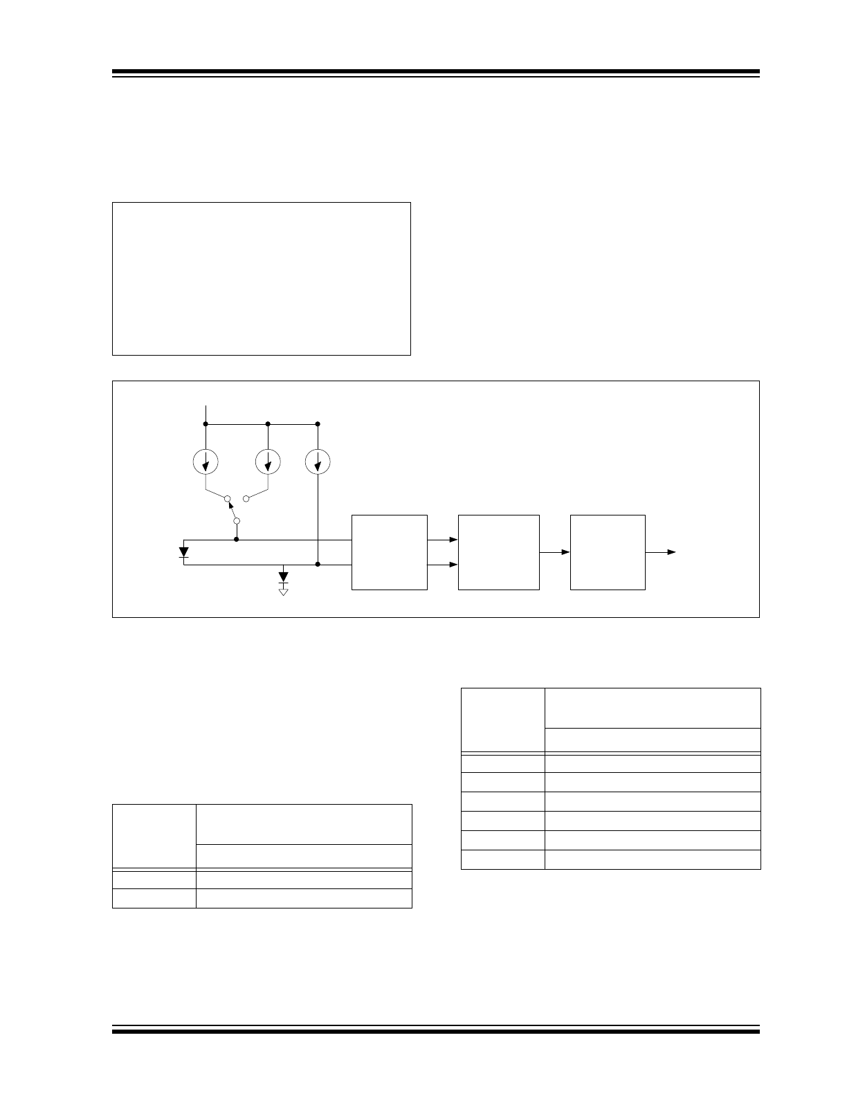
4.1
Temperature Monitors
Thermal diode temperature measurements are based
on the change in forward bias voltage (
V
BE
) of a diode
when operated at two different currents:
EQUATION 4-1:
The change in
V
BE
voltage is proportional to absolute
temperature T.
Figure 4-2
shows a detailed block diagram of the
temperature measurement circuit. The EMC1001
incorporates switched capacitor technology that
integrates the temperature diode
V
BE
from different
bias currents. The negative terminal (DN) for the
temperature diode is internally biased with a forward
diode voltage referenced to ground.
The advantages of this architecture over Nyquist rate
direct-conversion ADC (FLASH) or successive approx-
imation register (SAR) converters are superb linearity
and inherent noise immunity. The linearity can be
directly attributed to the delta-sigma ADC single-bit
comparator, while the noise immunity is achieved by
the ~20 ms integration time which translates to 50 Hz
input noise bandwidth.
FIGURE 4-2:
Detailed Block Diagram.
4.2
Temperature Measurement
Results and Data
The 10-bit temperature measurement results are
stored in temperature value registers.
Table 4-1
shows
the two’s complement temperature data format with an
LSB equivalent to 0.25°C.
V
B E
V
BE_HIGH
V
BE_LOW
kT
q
----------
I
HIGH
I
LOW
--------------
ln
=
–
=
Where:
k = Boltzmann’s Constant
T = Absolute Temperature in Kelvin
q = Electron Charge
= Diode Ideality Factor
Delta V
BE
Sample
&
Hold
I
BIAS
I
LOW
I
HIGH
1-bit
Delta-Sigma
Modulator
Digital
Averaging
Filter
V
DD
Internal or
Remote Diode
Bias
Diode
10-bit Output
TABLE 4-1:
TEMPERATURE DATA
FORMAT
Temperature
Valid Range
-40°C to +125°C
Two’s Complement
-0.25°C
1111 1111 11
(
1
)
0.0°C
0000 0000 00
Note 1:
Temperature measurement returns
1100 0000 00
for all temperatures
-64.00°C.
2:
Temperature measurement returns
0111 1111 11
for all temperatures
+127.75°C.
+0.25°C
0000 0000 01
+0.50°C
0000 0000 10
+0.75°C
0000 0000 11
+1°C
0000 0001 00
...
...
+125°C
0111 1101 00
(
2
)
TABLE 4-1:
TEMPERATURE DATA
FORMAT (CONTINUED)
Temperature
Valid Range
-40°C to +125°C
Two’s Complement
Note 1:
Temperature measurement returns
1100 0000 00
for all temperatures
-64.00°C.
2:
Temperature measurement returns
0111 1111 11
for all temperatures
+127.75°C.
EMC1001
DS20005411A-page 10
2015 Microchip Technology Inc.
The eight most significant bits are stored in the
Temperature Value High Byte register and the two least
significant bits stored in the Temperature Value Low
Byte register as outlined in
Table 4-2
. The six LSB
positions of the Temperature Value Low Byte register
always read zero. In
Table 4-2
, the upper case “B”
shows the bit position of a 16-bit word created by
concatenating the High Byte and Low Byte, and the
lower case “b” shows the bit position in the 10-bit value.
4.3
ALERT/THERM2 Output
The ALERT/THERM2 output asserts if an out-of-limit
measurement is detected (T
A
low limit or T
A
> high
limit). The ALERT/THERM2 pin is an open-drain output
and requires a pull-up resistor to V
DD
. The
ALERT/THERM2 pin can be used as an SMBALERT#,
or may be configured as a second THERM output.
As described in the SMBus specification, an SMBus
slave may inform the SMBus master that it wants to talk
by asserting the SMBALERT# signal. One or more
ALERT outputs can be hardwired together as a
wired-OR bus to a common input.
The ALERT/THERM2 pin resets when the EMC1001
responds to an alert response address
(ARA = 0001 100) sent by the host, and if the out-of-
limit condition no longer exists, but it does not reset if
the error condition remains. The ALERT/THERM2 pin
can be masked so that it will not assert in the event of
an out-of-limit temperature measurement, except when
it is configured as a second THERM pin.
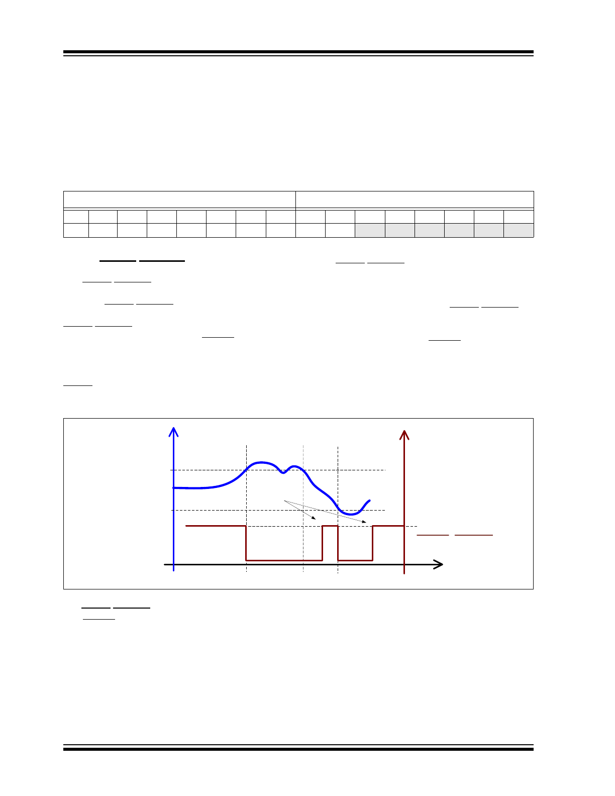
FIGURE 4-3:
ALERT Response to Temperature Limits Exceeded.
The ALERT/THERM2 pin can be configured as a sec-
ond THERM pin that asserts when the temperature
measurement exceeds the Temperature High Limit
value. The output will not de-assert until the tempera-
ture drops below the Temperature High Limit, minus the
THERM Hysteresis value.
TABLE 4-2:
BIT POSITION OF TWO BYTE VALUES
High Byte
Low Byte
B15
B14
B13
B12
B11
B10
B9
B8
B7
B6
B5
B4
B3
B2
B1
B0
b9
b8
b7
b6
b5
b4
b3
b2
b1
b0
0
0
0
0
0
0
Temp
Time
Temperature High Limit
Temperature Low Limit
ALERT/THERM2
Logic High
Logic
Level
SMBus ARA