
SMSC EMC1001
DATASHEET
Revision 1.6 (01-29-07)
Datasheet
PRODUCT FEATURES
EMC1001
1.5°C SMBus
Temperature Sensor in
Miniature SOT-23
General Description
The EMC1001 is a tiny SMBus temperature sensor with
±1.5
°
C accuracy and two interrupts. Packaged in a
SOT23-6, the EMC1001 provides an accurate, low-cost,
low-current, solution for critical temperature monitoring
in a PC or embedded applications.
The EMC1001 generates two separate interrupts with
programmable thermal trip points. The
THERM
output
operates as a thermostat with programmable threshold
and hysteresis. The
ALERT
output can be configured
as a maskable SMBus alert with programmable
window comparator limits, or as a second
THERM
output. An efficient fan control system can be created
since this output may be used to control a fan.
A power down mode extends battery life in portable
applications.
Each part number may be configured to respond to one
of four separate SMBus addresses.
Features
Self Contained Internal Temperature Sensor
—
0.25
°C resolution
—
±1.5°C Accuracy 40°C to 85°C
Small 6-lead SOT lead-free RoHS compliant
packages
SMBus address selected by external resistor
—
Select 1 of 4 per package, 8 addresses available
Maskable Interrupt using
ALERT
One-shot Command during standby
Low Power, 3.0V to 3.6V Supply
—
47uA at 0.0625 Conversions per Second (Typical)
—
4.8uA in Standby (Typical)
SMBus 2.0 Compliant interface
Programmable temperature conversion rate
Applications
Desktop and Notebook Computers
Thermostats
Smart batteries
Industrial/Automotive
Other Electronic Systems
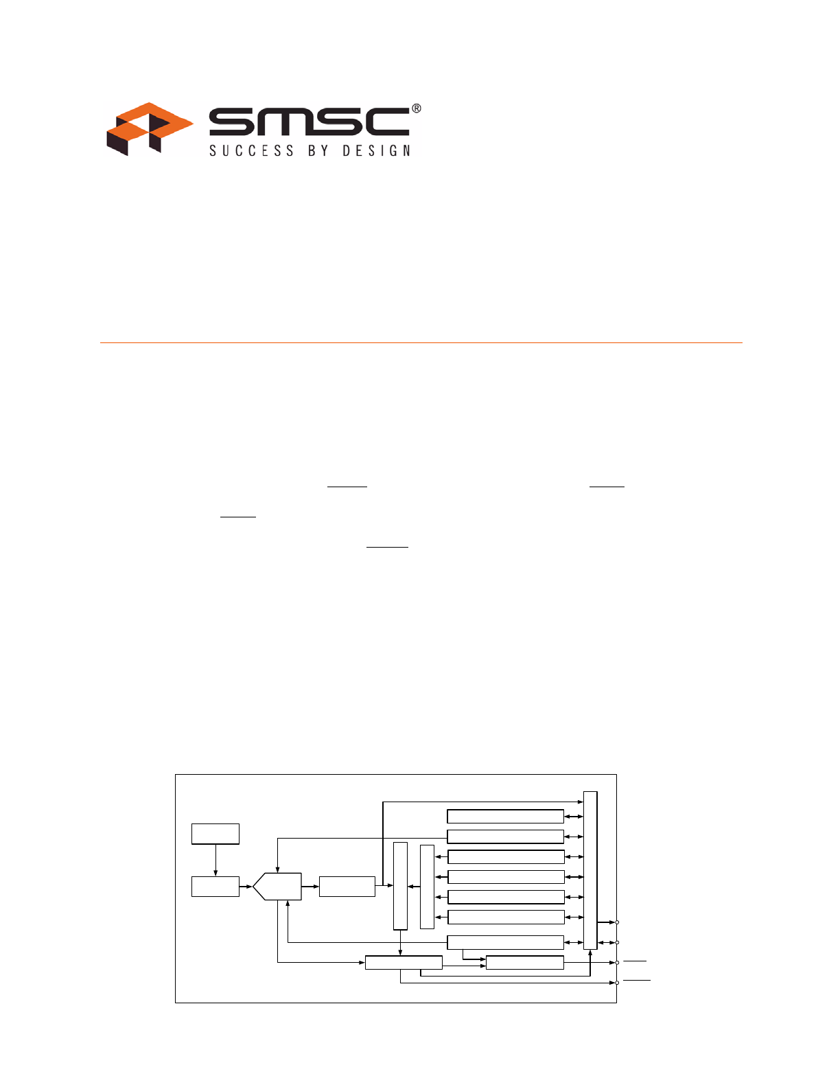
Simplified Block Diagram
EMC1001
Internal
Temp Diode
Switching
Current
SMCLK
Di
gita
l Mu
x
Li
mit Co
mpa
rat
or
High Limit Registers
THERM Hysteresis Register
Low Limit Registers
THERM Limit Register
Address Pointer Register
Conversion Rate Register
Interrupt Masking
Status Register
Configuration Register
SM
B
u
s
In
te
rf
a
c
e
Temperature
Register
ALERT
SMDATA
10-bit
delta-sigma
ADC
THERM

Order Number(s):
EMC1001-AFZQ-TR for 6 pin, SOT 23 Lead-Free RoHS compliant package
(tape and reel)
EMC1001-1-AFZQ-TR for 6 pin, SOT 23 Lead-Free RoHS compliant package
(alternate addresses, tape and reel)
See
Table 1.2, "SMBus Address Configuration Information," on page 3
Reel size is 8,000 pieces.
80 ARKAY DRIVE, HAUPPAUGE, NY 11788 (631) 435-6000, FAX (631) 273-3123
Copyright © 2007 SMSC or its subsidiaries. All rights reserved.
Circuit diagrams and other information relating to SMSC products are included as a means of illustrating typical applications. Consequently, complete information sufficient for
construction purposes is not necessarily given. Although the information has been checked and is believed to be accurate, no responsibility is assumed for inaccuracies. SMSC
reserves the right to make changes to specifications and product descriptions at any time without notice. Contact your local SMSC sales office to obtain the latest specifications
before placing your product order. The provision of this information does not convey to the purchaser of the described semiconductor devices any licenses under any patent
rights or other intellectual property rights of SMSC or others. All sales are expressly conditional on your agreement to the terms and conditions of the most recently dated
version of SMSC's standard Terms of Sale Agreement dated before the date of your order (the "Terms of Sale Agreement"). The product may contain design defects or errors
known as anomalies which may cause the product's functions to deviate from published specifications. Anomaly sheets are available upon request. SMSC products are not
designed, intended, authorized or warranted for use in any life support or other application where product failure could cause or contribute to personal injury or severe property
damage. Any and all such uses without prior written approval of an Officer of SMSC and further testing and/or modification will be fully at the risk of the customer. Copies of
this document or other SMSC literature, as well as the Terms of Sale Agreement, may be obtained by visiting SMSC’s website at http://www.smsc.com. SMSC is a registered
trademark of Standard Microsystems Corporation (“SMSC”). Product names and company names are the trademarks of their respective holders.
SMSC DISCLAIMS AND EXCLUDES ANY AND ALL WARRANTIES, INCLUDING WITHOUT LIMITATION ANY AND ALL IMPLIED WARRANTIES OF MERCHANTABILITY,
FITNESS FOR A PARTICULAR PURPOSE, TITLE, AND AGAINST INFRINGEMENT AND THE LIKE, AND ANY AND ALL WARRANTIES ARISING FROM ANY COURSE
OF DEALING OR USAGE OF TRADE. IN NO EVENT SHALL SMSC BE LIABLE FOR ANY DIRECT, INCIDENTAL, INDIRECT, SPECIAL, PUNITIVE, OR CONSEQUENTIAL
DAMAGES; OR FOR LOST DATA, PROFITS, SAVINGS OR REVENUES OF ANY KIND; REGARDLESS OF THE FORM OF ACTION, WHETHER BASED ON CONTRACT;
TORT; NEGLIGENCE OF SMSC OR OTHERS; STRICT LIABILITY; BREACH OF WARRANTY; OR OTHERWISE; WHETHER OR NOT ANY REMEDY OF BUYER IS HELD
TO HAVE FAILED OF ITS ESSENTIAL PURPOSE, AND WHETHER OR NOT SMSC HAS BEEN ADVISED OF THE POSSIBILITY OF SUCH DAMAGES.
1.5°C SMBus Temperature Sensor in Miniature SOT-23
Datasheet
Revision 1.6 (01-29-07)
2
SMSC EMC1001
DATASHEET
1.5°C SMBus Temperature Sensor in Miniature SOT-23
Datasheet
SMSC EMC1001
3
Revision 1.6 (01-29-07)
DATASHEET
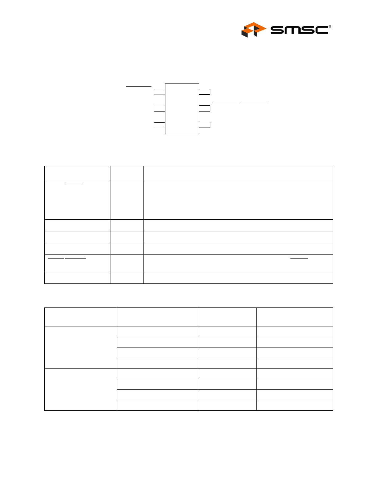
Chapter 1 Pin Configuration
Figure 1.1 EMC1001 Pin Configuration
Note 1.1
This value must be greater than 1k
Ω ±5% and less than or equal to 7.5kΩ ±5%.
Note 1.2
The pull-up resistor must be connected to V
DD
(pin 1), and the total capacitance on this
pin must be less than 100pF.
Table 1.1 Pin Description
PIN
PIN NO.
DESCRIPTION
ADDR/
THERM
1
Logic output that can be used to turn on/off a fan or throttle a CPU clock
in the event of an over-temperature condition. This is an open-drain
output. This pin is sampled following power up and the value of the pull
up resistor determines the SMBus slave address per
Table 1.2
.Total
capacitance on this pin must not exceed 100 pF, and the pull-up resistor
must be connected to the same supply voltage as V
DD
GND
2
Ground.
V
DD
3
Supply Voltage, 3.0V to 3.6V.
SMCLK
4
SMBus clock input.
ALERT
/
THERM2
5
Logic output used as interrupt, SMBus alert or as a second
THERM
output.
This is an open-drain output.
SMDATA
6
SMBus data input/output, open drain output.
Table 1.2 SMBus Address Configuration Information
PART NUMBER
ADDR/THERM
PULL-UP RESISTOR
SMBUS
ADDRESS
PACKAGE
DESCRIPTION
EMC1001
7.5k
Ω ±5%
Note 1.1
,
Note 1.2
1001 000b
6-Lead SOT-23
12k
Ω ±5%
Note 1.2
1001 001b
6-Lead SOT-23
20k
Ω ±5%
Note 1.2
0111 000b
6-Lead SOT-23
33k
Ω ±5%
Note 1.2
0111 001b
6-Lead SOT-23
EMC1001-1
7.5k
Ω ±5%
Note 1.1
,
Note 1.2
1001 010b
6-Lead SOT-23
12k
Ω ±5%
Note 1.2
1001 011b
6-Lead SOT-23
20k
Ω ±5%
Note 1.2
0111 010b
6-Lead SOT-23
33k
Ω ±5%
Note 1.2
0111 011b
6-Lead SOT-23
6
4
1
2
3
GND
V
DD
SMDATA
SMCLK
5
ADDR/THERM
ALERT/THERM2

1.5°C SMBus Temperature Sensor in Miniature SOT-23
Datasheet
Revision 1.6 (01-29-07)
4
SMSC EMC1001
DATASHEET
Note: Stresses above those listed could cause damage to the device. This is a stress rating only
and functional operation of the device at any other condition above those indicated in the
operation sections of this specification is not implied. When powering this device from
laboratory or system power supplies, it is important that the Absolute Maximum Ratings not be
exceeded or device failure can result. Some power supplies exhibit voltage spikes on their
outputs when the AC power is switched on or off. In addition, voltage transients on the AC
power line may appear on the DC output. If this possibility exists, it is suggested that a clamp
circuit be used.
Table 1.3 Absolute Maximum Ratings
PARAMETER
RATING
UNIT
Supply Voltage V
DD
-0.3 to 5.0
V
Voltage on
ALERT
/
THERM2,
SMDATA and SMCLK
pins
-0.3 to 5.5
V
Voltage on any other pin
-0.3 to V
DD
+0.3
V
Operating Temperature Range
-25 to +125
°C
Storage Temperature Range
-55 to +150
°C
Lead Temperature Range
Refer to JEDEC
Spec. J-STD-020
Package Thermal Characteristics for SOT23-6
Power Dissipation
TBD
mW @ 70
o
C
Thermal Resistance
111.5
o
C/W
ESD Rating, All Pins (Human Body Model)
2000
V
1.5°C SMBus Temperature Sensor in Miniature SOT-23
Datasheet
SMSC EMC1001
5
Revision 1.6 (01-29-07)
DATASHEET
Chapter 2 Electrical Characteristics
Table 2.1 Electrical Characteristics
V
DD
=3.0V to 3.6V, T
A
= -25
°C to +125°C, Typical values at T
A
= 27
°C unless otherwise noted
PARAMETER
SYMBOL
MIN
TYP
MAX
UNITS
CONDITIONS
DC Power
Supply Voltage
V
DD
3.0
3.3
3.6
V
Average Operating Current
I
DD
47
TBD
μA
0.0625 conversion/s
See
Table 4.6,
"Conversion Rates,"
on page 14
I
PD
4.8
10
μA
Standby mode
Temperature Measurement
Accuracy
±0.5
±1.5
°C
40
°C≤T
A
≤85°C
±1
±3
°C
-25
°C≤T
A
≤125°C
Resolution
0.25
°C
Conversion Time
26
ms
Voltage Tolerance
Voltage at pin (ADDR/
THERM,
)
V
TOL
-0.3
3.6
V
Voltage at pin (
ALERT
/
THERM2,
SMDATA,SMCLK)
V
TOL
-0.3
5.5
V
Digital Outputs (
ADDR
/
THERM
,
ALERT
/
THERM2
)
Output Low Voltage
V
OL
0.4
V
I
OUT
=-4mA
High Level Leakage Current
I
OH
0.1
1
μ
A
V
OUT
=V
DD
SMBus Interface (SMDATA,SMCLK)
Input High Level
V
IH
2.0
V
Input Low Level
V
IL
0.8
V
Input High/Low Current
I
IH
/I
IL
-1
1
μ
A
Hysteresis
500
mV
Input Capacitance
5
pF
Output Low Sink Current
6
mA
SMDATA = 0.6V
SMBus Timing
Clock Frequency
F
SMB
10
400
kHz
Spike Suppression
50
ns

1.5°C SMBus Temperature Sensor in Miniature SOT-23
Datasheet
Revision 1.6 (01-29-07)
6
SMSC EMC1001
DATASHEET
Note 2.1
300nS rise time max is required for 400kHz bus operation. For lower clock frequencies,
the maximum rise time is (0.1/F
SMB
)+50nS
Bus free time Start to Stop
T
BUF
1.3
μ
s
Hold time Start
T
HD:STA
0.6
μ
s
Setup time Start
T
SU:STA
0.6
μ
s
Setup time Stop
T
SU:STO
0.6
μ
s
Data Hold Time
T
HD:DAT
0.3
μ
s
Data Setup Time
T
SU:DAT
100
ns
Clock Low Period
T
LOW
1.3
μ
s
Clock High Period
T
HIGH
0.6
μ
s
Clock/Data Fall Time
T
F
*
300
ns
*Min = 20+0.1C
b
ns
Clock/Data Rise Time
T
R
*
300
Note
2.1
ns
*Min = 20+0.1C
b
ns
Capacitive Load (each bus line)
C
b
0.6
400
pF
Table 2.1 Electrical Characteristics (continued)
V
DD
=3.0V to 3.6V, T
A
= -25
°C to +125°C, Typical values at T
A
= 27
°C unless otherwise noted
PARAMETER
SYMBOL
MIN
TYP
MAX
UNITS
CONDITIONS
1.5°C SMBus Temperature Sensor in Miniature SOT-23
Datasheet
SMSC EMC1001
7
Revision 1.6 (01-29-07)
DATASHEET
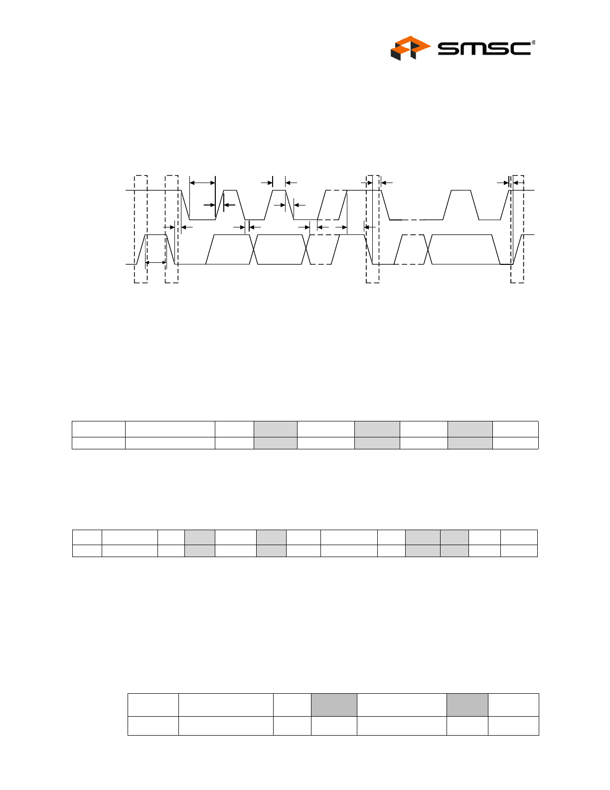
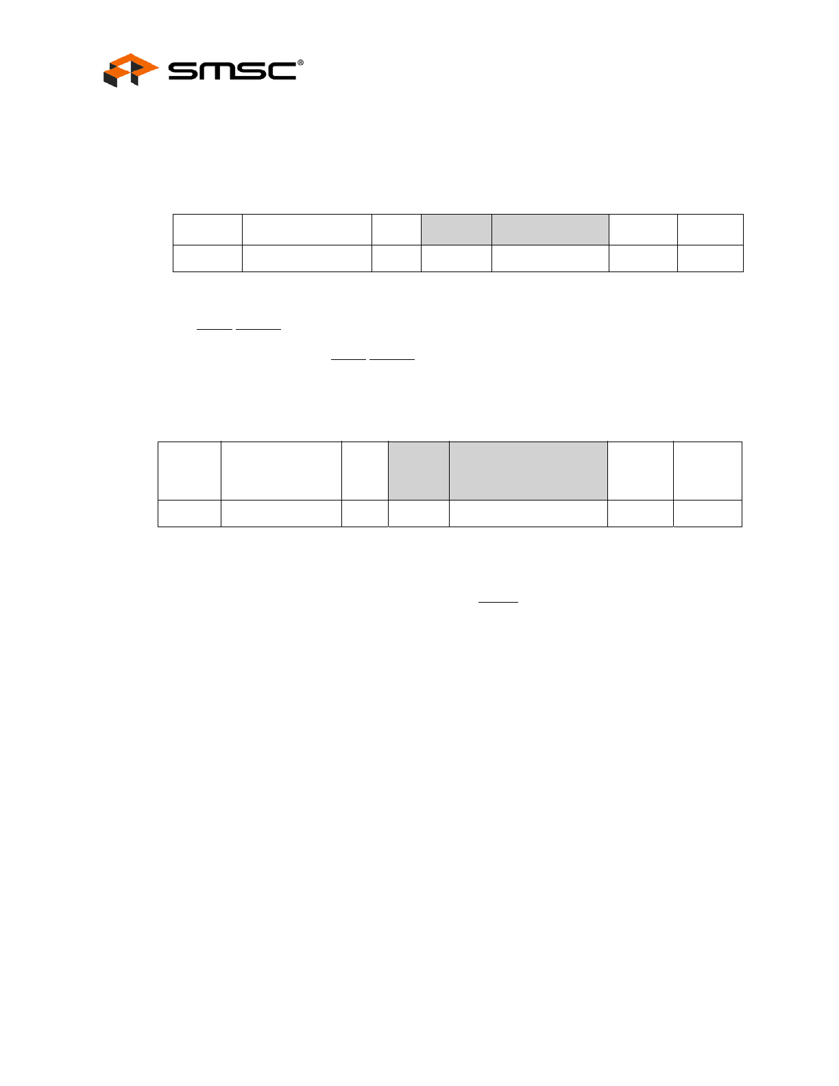
Chapter 3 System Management Bus Interface Protocol
A host controller, such as an SMSC I/O controller, communicates with the EMC1001 via the two wire
serial interface named SMBus. The SMBus interface is used to read and write registers in the
EMC1001, which is a slave-only device. A detailed timing diagram is shown in
Figure 3.1
.
Figure 3.1 System Management Bus Timing Diagram
The EMC1001 implements a subset of the SMBus specification and supports Write Byte, Read Byte,
Send Byte, Receive Byte, and Alert Response Address protocols. as shown. In the tables that describe
the protocol, the “gray” columns indicate that the slave is driving the bus.
3.1
Write Byte
The Write Byte protocol is used to write one byte of data to the registers as shown below:
3.2
Read Byte
The Read Byte protocol is used to read one byte of data from the registers as shown below:
3.3
Send Byte
The Send Byte protocol is used to set the Internal Address Register to the correct Address. The Send
Byte can be followed by the Receive Byte protocol described below in order to read data from the
register. The send byte protocol cannot be used to write data - if data is to be written to a register then
the write byte protocol must be used as described in subsection above. The send byte protocol is shown
in
Table 3.3
.
Table 3.1 SMBus Write Byte Protocol
START
SLAVE ADDRESS
WR
ACK
COMMAND
ACK
DATA
ACK
STOP
1
7
1
1
8
1
8
1
1
Table 3.2 SMBus Read Byte Protocol
START
SLAVE ADDRESS
WR
ACK
COMMAND
ACK
START
SLAVE ADDRESS
RD
ACK
DATA
NACK
STOP
1
7
1
1
8
1
1
7
1
1
8
1
1
Table 3.3 SMBus Send Byte Protocol
FIELD:
START
SLAVE ADDR
WR
ACK
REG. ADDR
ACK
STOP
Bits:
1
7
1
1
8
1
1
S M D A TA
S M C LK
T
LO W
T
R
T
H IG H
T
F
T
B U F
T
H D :S TA
P
S
S - S tart C ondition
P - S top C ondition
T
H D :D A T
T
S U :D A T
T
S U :S TA
T
H D :S TA
P
T
S U :S TO
S
1.5°C SMBus Temperature Sensor in Miniature SOT-23
Datasheet
Revision 1.6 (01-29-07)
8
SMSC EMC1001
DATASHEET
3.4
Receive Byte
The Receive Byte protocol is used to read data from a register when the internal register address pointer
is known to be at the right location (e.g. set via Send Byte). This can be used for consecutive reads of
the same register as shown below:
3.5
Alert Response Address
The
ALERT
/
THERM2
output can be used as an SMBALERT# as described in
4.3, "ALERT/THERM2
Output," on page 11
. The Alert Response Address is polled by the Host whenever it detects an
SMBALERT#, i.e. when the
ALERT
/
THERM2
pin is asserted. The EMC1001 will acknowlege the Alert
Response Address and respond with its device address as shown below.
3.6
SMBus Addresses
The EMC1001 is available in two versions, each of which has four 7-bit slave addresses that are
enabled based on the pull-up resistor on the
ADDR
/
THERM
pin. The value of this pull up resistor
determines the slave address per
Table 1.2 on page 3
. Attempting to communicate with the EMC1001
SMBus interface with an invalid slave address or invalid protocol results in no response from the device
and does not affect its register contents. The EMC1001 supports stretching of the SMCLK signal by
other devices on the SMBus but will not perform this operation itself. The EMC1001 has an SMBus
timeout feature. Bit 7 of the SMBus Timeout Enable register enables this function when set to 1 (the
default setting is 0). When this feature is enabled, the SMBus will timeout after approximately 25ms
of inactivity.
Table 3.4 SMBus Receive Byte Protocol
FIELD:
START
SLAVE ADDR
RD
ACK
REG. DATA
NACK
STOP
Bits:
1
7
1
1
8
1
1
Table 3.5 Modified SMBus Receive Byte Protocol Response to ARA
FIELD:
START
ALERT
RESPONSE
ADDRESS
RD
ACK
EMC1001 SLAVE
ADDRESS NACK
STOP
Bits:
1
7
1
1
8
1
1
1.5°C SMBus Temperature Sensor in Miniature SOT-23
Datasheet
SMSC EMC1001
9
Revision 1.6 (01-29-07)
DATASHEET
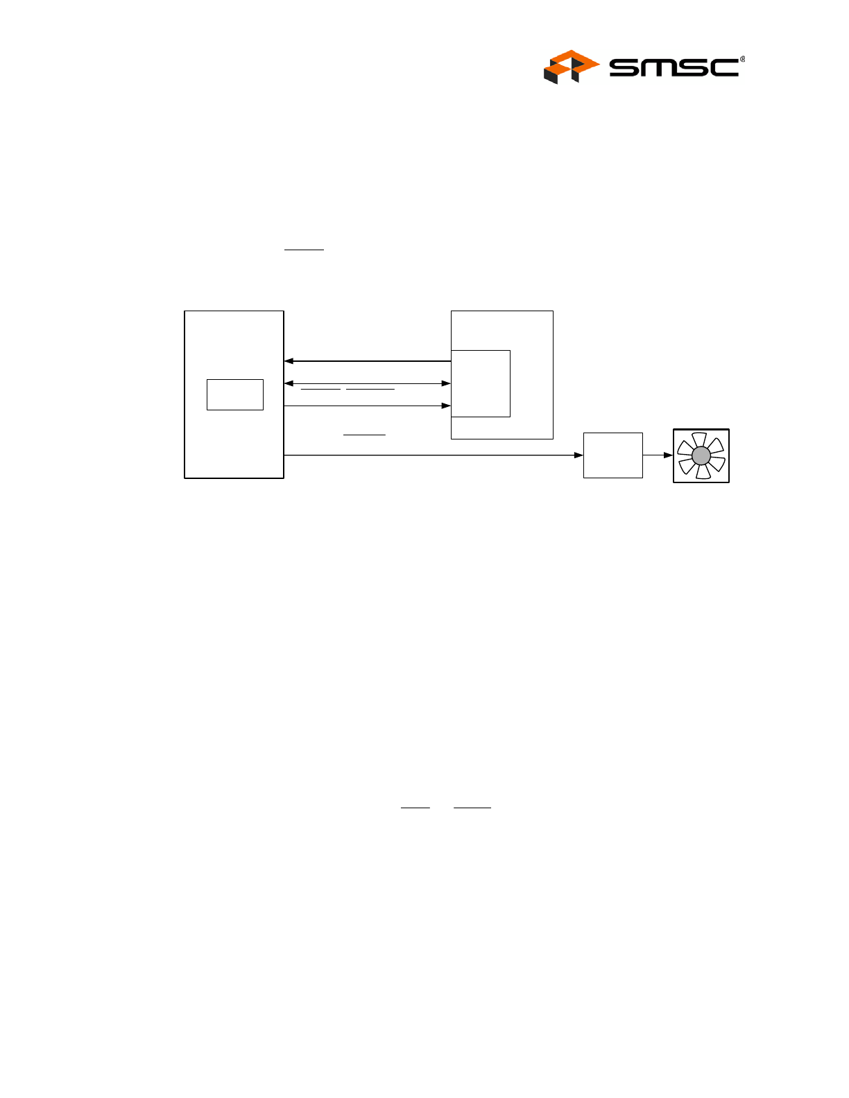
Chapter 4 Product Description
The EMC1001 is an SMBus temperature that monitors a single temperature zone. Thermal
management is performed in cooperation with a host device. The host reads the temperature data from
the EMC1001 and takes appropriate action such as controlling fan speed or processor clock frequency.
The EMC1001 has programmable temperature limit registers that define a safe operating window. After
the host has configured the temperature limits, the EMC1001 can operate as a free-running
independent watchdog to warn the host of temperature hot spots without requiring the host to poll the
device. The
ADDR
/
THERM
output can be used to control a fan without host intervention.
Figure 4.1 Controlling a fan without host intervention.
The
EMC1001
has
two basic modes of operation:
Run Mode: In this mode, the EMC1001 continuously converts temperature data and updates its
registers. The rate of temperature conversion is configured as shown in
Section 4.9 on page 14
.
Standby Mode: In this mode, the EMC1001 is placed in standby to conserve power as described
in
Section 4.5 on page 12
.
4.1
Temperature Monitors
Thermal diode temperature measurements are based on the change in forward bias voltage (
ΔV
BE
) of
a diode when operated at two different currents:
The change in
Δ
V
BE
voltage is proportional to absolute temperature T.
where:
k = Boltzmann’s constant
T = absolute temperature in Kelvin
q = electron charge
η
= diode ideality factor
ADDR/THERM
ALERT/THERM2
EMC1001
Host
Fan
Driver
SMDATA
Internal
Diode
SMCLK
SMBus
Interface
⎟⎟
⎠
⎞
⎜⎜
⎝
⎛
=
−
=
Δ
LOW
HIGH
LOW
BE
HIGH
BE
BE
I
I
q
kT
V
V
V
ln
_
_
η
1.5°C SMBus Temperature Sensor in Miniature SOT-23
Datasheet
Revision 1.6 (01-29-07)
10
SMSC EMC1001
DATASHEET
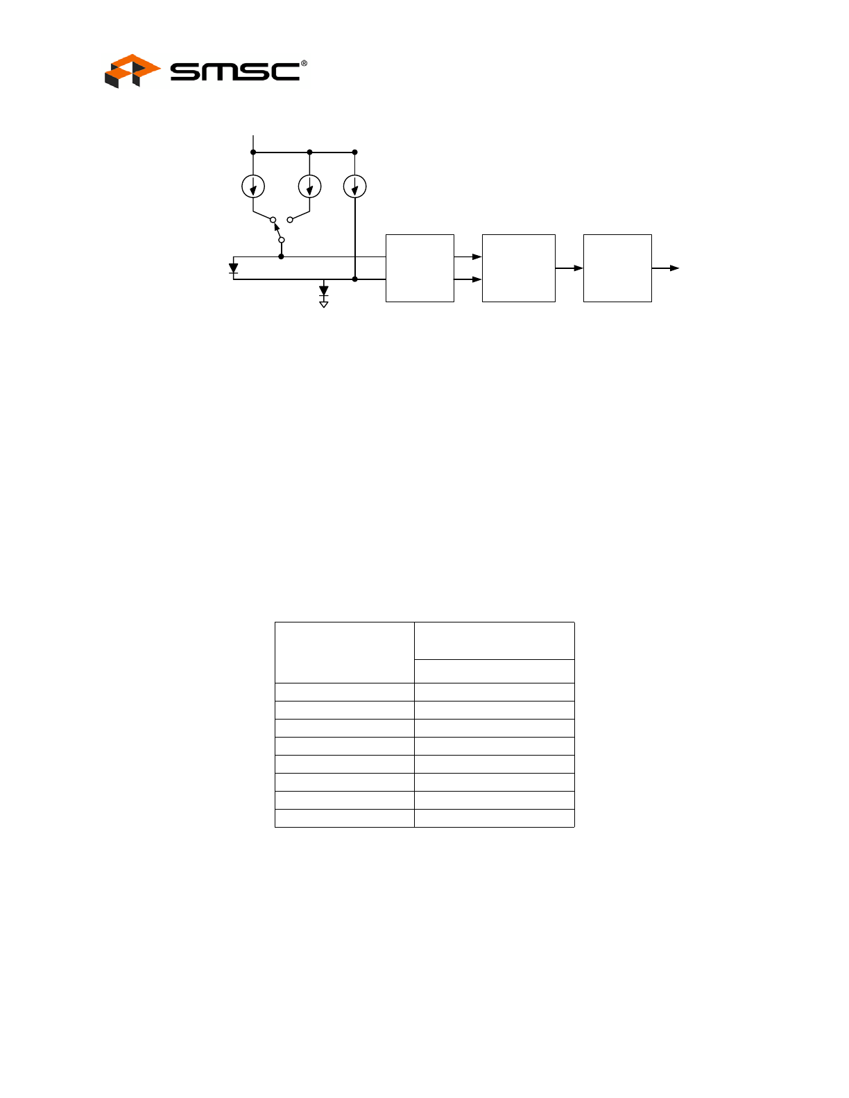
Figure 4.2 Detailed Block Diagram
Figure 4.2
shows a detailed block diagram of the temperature measurement circuit. The EMC1001
incorporates switched capacitor technology that integrates the temperature diode
ΔV
BE
from different
bias currents. The negative terminal, DN, for the temperature diode is internally biased with a forward
diode voltage referenced to ground.
The advantages of this architecture over Nyquist rate FLASH or SAR converters are superb linearity
and inherent noise immunity. The linearity can be directly attributed to the delta-sigma ADC single-bit
comparator while the noise immunity is achieved by the ~20ms integration time which translates to
50Hz input noise bandwidth.
4.2
Temperature Measurement Results and Data
The 10-bit temperature measurement results are stored in temperature value registers.
Table 4.1
shows the two’s complement temperature data format with an LSB equivalent to 0.25
°
C.
Note 4.1
Temperature measurement returns 1100 0000 00 for all temperatures
≤ -64.00°C
Note 4.2
Temperature measurement returns 0111 1111 11 for all temperatures
≥ +127.75
°
C
The eight most significant bits are stored in the Temperature Value High Byte register and the two least
significant bits stored in the Temperature Value Low Byte register as outlined in
Table 4.2
. The six LSB
positions of the Temperature Value Low Byte register always read zero. In
Table 4.2
, the upper case
Table 4.1 Temperature Data Format
TEMPERATURE
VALID RANGE
–40
°
C TO 125
°
C
TWO’S COMPLEMENT
-0.25
°
C
1111 1111 11
Note 4.1
0.0
°
C
0000 0000 00
+0.25
°
C
0000 0000 01
+0.50
°
C
0000 0000 10
+0.75
°
C
0000 0000 11
+1
°
C
0000 0001 00
+125
°
C
0111 1101 00
Note 4.2
Delta Vbe
Sample
&
Hold
I
bias
I
low
I
high
1-bit
delta-sigma
Modulator
Digital
Averaging
Filter
V
DD
Internal or
Remote Diode
Bias
Diode
10-bit Output
SMSC EMC1001
DATASHEET
Revision 1.6 (01-29-07)
Datasheet
PRODUCT FEATURES
EMC1001
1.5°C SMBus
Temperature Sensor in
Miniature SOT-23
General Description
The EMC1001 is a tiny SMBus temperature sensor with
±1.5
°
C accuracy and two interrupts. Packaged in a
SOT23-6, the EMC1001 provides an accurate, low-cost,
low-current, solution for critical temperature monitoring
in a PC or embedded applications.
The EMC1001 generates two separate interrupts with
programmable thermal trip points. The
THERM
output
operates as a thermostat with programmable threshold
and hysteresis. The
ALERT
output can be configured
as a maskable SMBus alert with programmable
window comparator limits, or as a second
THERM
output. An efficient fan control system can be created
since this output may be used to control a fan.
A power down mode extends battery life in portable
applications.
Each part number may be configured to respond to one
of four separate SMBus addresses.
Features
Self Contained Internal Temperature Sensor
—
0.25
°C resolution
—
±1.5°C Accuracy 40°C to 85°C
Small 6-lead SOT lead-free RoHS compliant
packages
SMBus address selected by external resistor
—
Select 1 of 4 per package, 8 addresses available
Maskable Interrupt using
ALERT
One-shot Command during standby
Low Power, 3.0V to 3.6V Supply
—
47uA at 0.0625 Conversions per Second (Typical)
—
4.8uA in Standby (Typical)
SMBus 2.0 Compliant interface
Programmable temperature conversion rate
Applications
Desktop and Notebook Computers
Thermostats
Smart batteries
Industrial/Automotive
Other Electronic Systems
Simplified Block Diagram
EMC1001
Internal
Temp Diode
Switching
Current
SMCLK
Di
gita
l Mu
x
Li
mit Co
mpa
rat
or
High Limit Registers
THERM Hysteresis Register
Low Limit Registers
THERM Limit Register
Address Pointer Register
Conversion Rate Register
Interrupt Masking
Status Register
Configuration Register
SM
B
u
s
In
te
rf
a
c
e
Temperature
Register
ALERT
SMDATA
10-bit
delta-sigma
ADC
THERM
Order Number(s):
EMC1001-AFZQ-TR for 6 pin, SOT 23 Lead-Free RoHS compliant package
(tape and reel)
EMC1001-1-AFZQ-TR for 6 pin, SOT 23 Lead-Free RoHS compliant package
(alternate addresses, tape and reel)
See
Table 1.2, "SMBus Address Configuration Information," on page 3
Reel size is 8,000 pieces.
80 ARKAY DRIVE, HAUPPAUGE, NY 11788 (631) 435-6000, FAX (631) 273-3123
Copyright © 2007 SMSC or its subsidiaries. All rights reserved.
Circuit diagrams and other information relating to SMSC products are included as a means of illustrating typical applications. Consequently, complete information sufficient for
construction purposes is not necessarily given. Although the information has been checked and is believed to be accurate, no responsibility is assumed for inaccuracies. SMSC
reserves the right to make changes to specifications and product descriptions at any time without notice. Contact your local SMSC sales office to obtain the latest specifications
before placing your product order. The provision of this information does not convey to the purchaser of the described semiconductor devices any licenses under any patent
rights or other intellectual property rights of SMSC or others. All sales are expressly conditional on your agreement to the terms and conditions of the most recently dated
version of SMSC's standard Terms of Sale Agreement dated before the date of your order (the "Terms of Sale Agreement"). The product may contain design defects or errors
known as anomalies which may cause the product's functions to deviate from published specifications. Anomaly sheets are available upon request. SMSC products are not
designed, intended, authorized or warranted for use in any life support or other application where product failure could cause or contribute to personal injury or severe property
damage. Any and all such uses without prior written approval of an Officer of SMSC and further testing and/or modification will be fully at the risk of the customer. Copies of
this document or other SMSC literature, as well as the Terms of Sale Agreement, may be obtained by visiting SMSC’s website at http://www.smsc.com. SMSC is a registered
trademark of Standard Microsystems Corporation (“SMSC”). Product names and company names are the trademarks of their respective holders.
SMSC DISCLAIMS AND EXCLUDES ANY AND ALL WARRANTIES, INCLUDING WITHOUT LIMITATION ANY AND ALL IMPLIED WARRANTIES OF MERCHANTABILITY,
FITNESS FOR A PARTICULAR PURPOSE, TITLE, AND AGAINST INFRINGEMENT AND THE LIKE, AND ANY AND ALL WARRANTIES ARISING FROM ANY COURSE
OF DEALING OR USAGE OF TRADE. IN NO EVENT SHALL SMSC BE LIABLE FOR ANY DIRECT, INCIDENTAL, INDIRECT, SPECIAL, PUNITIVE, OR CONSEQUENTIAL
DAMAGES; OR FOR LOST DATA, PROFITS, SAVINGS OR REVENUES OF ANY KIND; REGARDLESS OF THE FORM OF ACTION, WHETHER BASED ON CONTRACT;
TORT; NEGLIGENCE OF SMSC OR OTHERS; STRICT LIABILITY; BREACH OF WARRANTY; OR OTHERWISE; WHETHER OR NOT ANY REMEDY OF BUYER IS HELD
TO HAVE FAILED OF ITS ESSENTIAL PURPOSE, AND WHETHER OR NOT SMSC HAS BEEN ADVISED OF THE POSSIBILITY OF SUCH DAMAGES.
1.5°C SMBus Temperature Sensor in Miniature SOT-23
Datasheet
Revision 1.6 (01-29-07)
2
SMSC EMC1001
DATASHEET
1.5°C SMBus Temperature Sensor in Miniature SOT-23
Datasheet
SMSC EMC1001
3
Revision 1.6 (01-29-07)
DATASHEET
Chapter 1 Pin Configuration
Figure 1.1 EMC1001 Pin Configuration
Note 1.1
This value must be greater than 1k
Ω ±5% and less than or equal to 7.5kΩ ±5%.
Note 1.2
The pull-up resistor must be connected to V
DD
(pin 1), and the total capacitance on this
pin must be less than 100pF.
Table 1.1 Pin Description
PIN
PIN NO.
DESCRIPTION
ADDR/
THERM
1
Logic output that can be used to turn on/off a fan or throttle a CPU clock
in the event of an over-temperature condition. This is an open-drain
output. This pin is sampled following power up and the value of the pull
up resistor determines the SMBus slave address per
Table 1.2
.Total
capacitance on this pin must not exceed 100 pF, and the pull-up resistor
must be connected to the same supply voltage as V
DD
GND
2
Ground.
V
DD
3
Supply Voltage, 3.0V to 3.6V.
SMCLK
4
SMBus clock input.
ALERT
/
THERM2
5
Logic output used as interrupt, SMBus alert or as a second
THERM
output.
This is an open-drain output.
SMDATA
6
SMBus data input/output, open drain output.
Table 1.2 SMBus Address Configuration Information
PART NUMBER
ADDR/THERM
PULL-UP RESISTOR
SMBUS
ADDRESS
PACKAGE
DESCRIPTION
EMC1001
7.5k
Ω ±5%
Note 1.1
,
Note 1.2
1001 000b
6-Lead SOT-23
12k
Ω ±5%
Note 1.2
1001 001b
6-Lead SOT-23
20k
Ω ±5%
Note 1.2
0111 000b
6-Lead SOT-23
33k
Ω ±5%
Note 1.2
0111 001b
6-Lead SOT-23
EMC1001-1
7.5k
Ω ±5%
Note 1.1
,
Note 1.2
1001 010b
6-Lead SOT-23
12k
Ω ±5%
Note 1.2
1001 011b
6-Lead SOT-23
20k
Ω ±5%
Note 1.2
0111 010b
6-Lead SOT-23
33k
Ω ±5%
Note 1.2
0111 011b
6-Lead SOT-23
6
4
1
2
3
GND
V
DD
SMDATA
SMCLK
5
ADDR/THERM
ALERT/THERM2
1.5°C SMBus Temperature Sensor in Miniature SOT-23
Datasheet
Revision 1.6 (01-29-07)
4
SMSC EMC1001
DATASHEET
Note: Stresses above those listed could cause damage to the device. This is a stress rating only
and functional operation of the device at any other condition above those indicated in the
operation sections of this specification is not implied. When powering this device from
laboratory or system power supplies, it is important that the Absolute Maximum Ratings not be
exceeded or device failure can result. Some power supplies exhibit voltage spikes on their
outputs when the AC power is switched on or off. In addition, voltage transients on the AC
power line may appear on the DC output. If this possibility exists, it is suggested that a clamp
circuit be used.
Table 1.3 Absolute Maximum Ratings
PARAMETER
RATING
UNIT
Supply Voltage V
DD
-0.3 to 5.0
V
Voltage on
ALERT
/
THERM2,
SMDATA and SMCLK
pins
-0.3 to 5.5
V
Voltage on any other pin
-0.3 to V
DD
+0.3
V
Operating Temperature Range
-25 to +125
°C
Storage Temperature Range
-55 to +150
°C
Lead Temperature Range
Refer to JEDEC
Spec. J-STD-020
Package Thermal Characteristics for SOT23-6
Power Dissipation
TBD
mW @ 70
o
C
Thermal Resistance
111.5
o
C/W
ESD Rating, All Pins (Human Body Model)
2000
V
1.5°C SMBus Temperature Sensor in Miniature SOT-23
Datasheet
SMSC EMC1001
5
Revision 1.6 (01-29-07)
DATASHEET
Chapter 2 Electrical Characteristics
Table 2.1 Electrical Characteristics
V
DD
=3.0V to 3.6V, T
A
= -25
°C to +125°C, Typical values at T
A
= 27
°C unless otherwise noted
PARAMETER
SYMBOL
MIN
TYP
MAX
UNITS
CONDITIONS
DC Power
Supply Voltage
V
DD
3.0
3.3
3.6
V
Average Operating Current
I
DD
47
TBD
μA
0.0625 conversion/s
See
Table 4.6,
"Conversion Rates,"
on page 14
I
PD
4.8
10
μA
Standby mode
Temperature Measurement
Accuracy
±0.5
±1.5
°C
40
°C≤T
A
≤85°C
±1
±3
°C
-25
°C≤T
A
≤125°C
Resolution
0.25
°C
Conversion Time
26
ms
Voltage Tolerance
Voltage at pin (ADDR/
THERM,
)
V
TOL
-0.3
3.6
V
Voltage at pin (
ALERT
/
THERM2,
SMDATA,SMCLK)
V
TOL
-0.3
5.5
V
Digital Outputs (
ADDR
/
THERM
,
ALERT
/
THERM2
)
Output Low Voltage
V
OL
0.4
V
I
OUT
=-4mA
High Level Leakage Current
I
OH
0.1
1
μ
A
V
OUT
=V
DD
SMBus Interface (SMDATA,SMCLK)
Input High Level
V
IH
2.0
V
Input Low Level
V
IL
0.8
V
Input High/Low Current
I
IH
/I
IL
-1
1
μ
A
Hysteresis
500
mV
Input Capacitance
5
pF
Output Low Sink Current
6
mA
SMDATA = 0.6V
SMBus Timing
Clock Frequency
F
SMB
10
400
kHz
Spike Suppression
50
ns
1.5°C SMBus Temperature Sensor in Miniature SOT-23
Datasheet
Revision 1.6 (01-29-07)
6
SMSC EMC1001
DATASHEET
Note 2.1
300nS rise time max is required for 400kHz bus operation. For lower clock frequencies,
the maximum rise time is (0.1/F
SMB
)+50nS
Bus free time Start to Stop
T
BUF
1.3
μ
s
Hold time Start
T
HD:STA
0.6
μ
s
Setup time Start
T
SU:STA
0.6
μ
s
Setup time Stop
T
SU:STO
0.6
μ
s
Data Hold Time
T
HD:DAT
0.3
μ
s
Data Setup Time
T
SU:DAT
100
ns
Clock Low Period
T
LOW
1.3
μ
s
Clock High Period
T
HIGH
0.6
μ
s
Clock/Data Fall Time
T
F
*
300
ns
*Min = 20+0.1C
b
ns
Clock/Data Rise Time
T
R
*
300
Note
2.1
ns
*Min = 20+0.1C
b
ns
Capacitive Load (each bus line)
C
b
0.6
400
pF
Table 2.1 Electrical Characteristics (continued)
V
DD
=3.0V to 3.6V, T
A
= -25
°C to +125°C, Typical values at T
A
= 27
°C unless otherwise noted
PARAMETER
SYMBOL
MIN
TYP
MAX
UNITS
CONDITIONS
1.5°C SMBus Temperature Sensor in Miniature SOT-23
Datasheet
SMSC EMC1001
7
Revision 1.6 (01-29-07)
DATASHEET
Chapter 3 System Management Bus Interface Protocol
A host controller, such as an SMSC I/O controller, communicates with the EMC1001 via the two wire
serial interface named SMBus. The SMBus interface is used to read and write registers in the
EMC1001, which is a slave-only device. A detailed timing diagram is shown in
Figure 3.1
.
Figure 3.1 System Management Bus Timing Diagram
The EMC1001 implements a subset of the SMBus specification and supports Write Byte, Read Byte,
Send Byte, Receive Byte, and Alert Response Address protocols. as shown. In the tables that describe
the protocol, the “gray” columns indicate that the slave is driving the bus.
3.1
Write Byte
The Write Byte protocol is used to write one byte of data to the registers as shown below:
3.2
Read Byte
The Read Byte protocol is used to read one byte of data from the registers as shown below:
3.3
Send Byte
The Send Byte protocol is used to set the Internal Address Register to the correct Address. The Send
Byte can be followed by the Receive Byte protocol described below in order to read data from the
register. The send byte protocol cannot be used to write data - if data is to be written to a register then
the write byte protocol must be used as described in subsection above. The send byte protocol is shown
in
Table 3.3
.
Table 3.1 SMBus Write Byte Protocol
START
SLAVE ADDRESS
WR
ACK
COMMAND
ACK
DATA
ACK
STOP
1
7
1
1
8
1
8
1
1
Table 3.2 SMBus Read Byte Protocol
START
SLAVE ADDRESS
WR
ACK
COMMAND
ACK
START
SLAVE ADDRESS
RD
ACK
DATA
NACK
STOP
1
7
1
1
8
1
1
7
1
1
8
1
1
Table 3.3 SMBus Send Byte Protocol
FIELD:
START
SLAVE ADDR
WR
ACK
REG. ADDR
ACK
STOP
Bits:
1
7
1
1
8
1
1
S M D A TA
S M C LK
T
LO W
T
R
T
H IG H
T
F
T
B U F
T
H D :S TA
P
S
S - S tart C ondition
P - S top C ondition
T
H D :D A T
T
S U :D A T
T
S U :S TA
T
H D :S TA
P
T
S U :S TO
S
1.5°C SMBus Temperature Sensor in Miniature SOT-23
Datasheet
Revision 1.6 (01-29-07)
8
SMSC EMC1001
DATASHEET
3.4
Receive Byte
The Receive Byte protocol is used to read data from a register when the internal register address pointer
is known to be at the right location (e.g. set via Send Byte). This can be used for consecutive reads of
the same register as shown below:
3.5
Alert Response Address
The
ALERT
/
THERM2
output can be used as an SMBALERT# as described in
4.3, "ALERT/THERM2
Output," on page 11
. The Alert Response Address is polled by the Host whenever it detects an
SMBALERT#, i.e. when the
ALERT
/
THERM2
pin is asserted. The EMC1001 will acknowlege the Alert
Response Address and respond with its device address as shown below.
3.6
SMBus Addresses
The EMC1001 is available in two versions, each of which has four 7-bit slave addresses that are
enabled based on the pull-up resistor on the
ADDR
/
THERM
pin. The value of this pull up resistor
determines the slave address per
Table 1.2 on page 3
. Attempting to communicate with the EMC1001
SMBus interface with an invalid slave address or invalid protocol results in no response from the device
and does not affect its register contents. The EMC1001 supports stretching of the SMCLK signal by
other devices on the SMBus but will not perform this operation itself. The EMC1001 has an SMBus
timeout feature. Bit 7 of the SMBus Timeout Enable register enables this function when set to 1 (the
default setting is 0). When this feature is enabled, the SMBus will timeout after approximately 25ms
of inactivity.
Table 3.4 SMBus Receive Byte Protocol
FIELD:
START
SLAVE ADDR
RD
ACK
REG. DATA
NACK
STOP
Bits:
1
7
1
1
8
1
1
Table 3.5 Modified SMBus Receive Byte Protocol Response to ARA
FIELD:
START
ALERT
RESPONSE
ADDRESS
RD
ACK
EMC1001 SLAVE
ADDRESS NACK
STOP
Bits:
1
7
1
1
8
1
1
1.5°C SMBus Temperature Sensor in Miniature SOT-23
Datasheet
SMSC EMC1001
9
Revision 1.6 (01-29-07)
DATASHEET
Chapter 4 Product Description
The EMC1001 is an SMBus temperature that monitors a single temperature zone. Thermal
management is performed in cooperation with a host device. The host reads the temperature data from
the EMC1001 and takes appropriate action such as controlling fan speed or processor clock frequency.
The EMC1001 has programmable temperature limit registers that define a safe operating window. After
the host has configured the temperature limits, the EMC1001 can operate as a free-running
independent watchdog to warn the host of temperature hot spots without requiring the host to poll the
device. The
ADDR
/
THERM
output can be used to control a fan without host intervention.
Figure 4.1 Controlling a fan without host intervention.
The
EMC1001
has
two basic modes of operation:
Run Mode: In this mode, the EMC1001 continuously converts temperature data and updates its
registers. The rate of temperature conversion is configured as shown in
Section 4.9 on page 14
.
Standby Mode: In this mode, the EMC1001 is placed in standby to conserve power as described
in
Section 4.5 on page 12
.
4.1
Temperature Monitors
Thermal diode temperature measurements are based on the change in forward bias voltage (
ΔV
BE
) of
a diode when operated at two different currents:
The change in
Δ
V
BE
voltage is proportional to absolute temperature T.
where:
k = Boltzmann’s constant
T = absolute temperature in Kelvin
q = electron charge
η
= diode ideality factor
ADDR/THERM
ALERT/THERM2
EMC1001
Host
Fan
Driver
SMDATA
Internal
Diode
SMCLK
SMBus
Interface
⎟⎟
⎠
⎞
⎜⎜
⎝
⎛
=
−
=
Δ
LOW
HIGH
LOW
BE
HIGH
BE
BE
I
I
q
kT
V
V
V
ln
_
_
η
1.5°C SMBus Temperature Sensor in Miniature SOT-23
Datasheet
Revision 1.6 (01-29-07)
10
SMSC EMC1001
DATASHEET
Figure 4.2 Detailed Block Diagram
Figure 4.2
shows a detailed block diagram of the temperature measurement circuit. The EMC1001
incorporates switched capacitor technology that integrates the temperature diode
ΔV
BE
from different
bias currents. The negative terminal, DN, for the temperature diode is internally biased with a forward
diode voltage referenced to ground.
The advantages of this architecture over Nyquist rate FLASH or SAR converters are superb linearity
and inherent noise immunity. The linearity can be directly attributed to the delta-sigma ADC single-bit
comparator while the noise immunity is achieved by the ~20ms integration time which translates to
50Hz input noise bandwidth.
4.2
Temperature Measurement Results and Data
The 10-bit temperature measurement results are stored in temperature value registers.
Table 4.1
shows the two’s complement temperature data format with an LSB equivalent to 0.25
°
C.
Note 4.1
Temperature measurement returns 1100 0000 00 for all temperatures
≤ -64.00°C
Note 4.2
Temperature measurement returns 0111 1111 11 for all temperatures
≥ +127.75
°
C
The eight most significant bits are stored in the Temperature Value High Byte register and the two least
significant bits stored in the Temperature Value Low Byte register as outlined in
Table 4.2
. The six LSB
positions of the Temperature Value Low Byte register always read zero. In
Table 4.2
, the upper case
Table 4.1 Temperature Data Format
TEMPERATURE
VALID RANGE
–40
°
C TO 125
°
C
TWO’S COMPLEMENT
-0.25
°
C
1111 1111 11
Note 4.1
0.0
°
C
0000 0000 00
+0.25
°
C
0000 0000 01
+0.50
°
C
0000 0000 10
+0.75
°
C
0000 0000 11
+1
°
C
0000 0001 00
+125
°
C
0111 1101 00
Note 4.2
Delta Vbe
Sample
&
Hold
I
bias
I
low
I
high
1-bit
delta-sigma
Modulator
Digital
Averaging
Filter
V
DD
Internal or
Remote Diode
Bias
Diode
10-bit Output