
2017 Microchip Technology Inc.
DS20005836A-page 1
MIC862
Features
• 8-Pin SOT-23 Package
• 3 MHz Gain-Bandwidth Product
• 5 MHz, –3 dB Bandwidth
• 31 µA Supply Current
• Rail-to-Rail Output
• Ground Sensing at Input
(Common-Mode-to-GND)
• Drives Large Capacitive Loads
• Unity Gain Stable
Applications
• Portable Equipment
• Medical Instruments
• PDAs
• Pagers
• Cordless Phones
• Consumer Electronics
General Description
The MIC862 is a dual low-power operational amplifier
in an SOT23-8 package. It is designed to operate in the
2V to 5V range, rail-to-rail output, with input
common-mode to ground. The MIC862 provides
3 MHz gain-bandwidth product while consuming only
31 µA supply current per channel.
With low supply voltage and 8-lead SOT-23 packaging,
MIC862 provides two channels as general-purpose
amplifiers for portable and battery-powered
applications. Its package provides the maximum
performance available while maintaining an extremely
slim form factor. The minimal power consumption of
this IC maximizes the battery life potential.
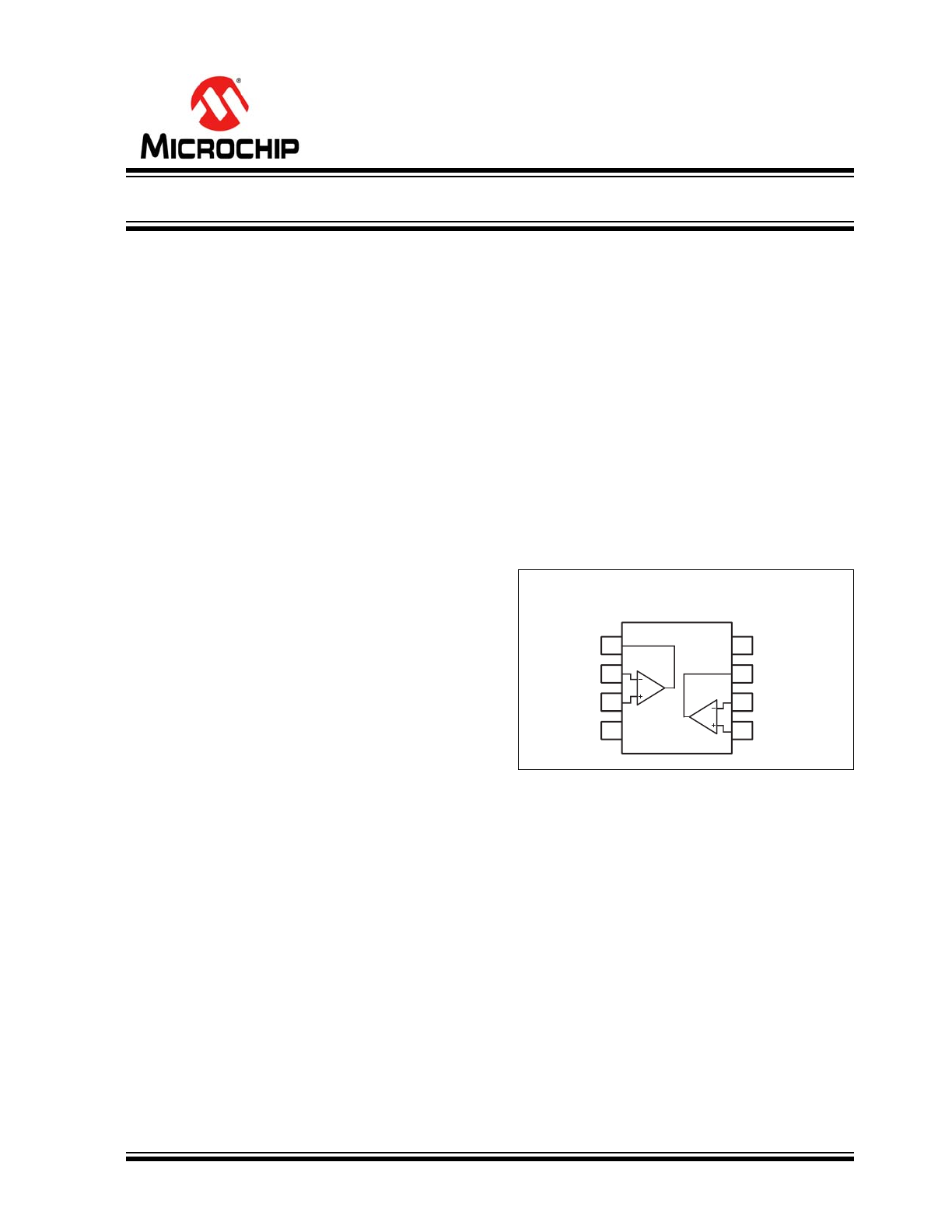
Package Type
MIC862
8-Pin SOT-23 (M8)
1
OUTA
INA–
INA+
V–
8
V+
OUTB
INB–
INB+
7
6
5
2
3
4
Dual Ultra-Low Power Op Amp in SOT-23-8
MIC862
DS20005836A-page 2
2017 Microchip Technology Inc.
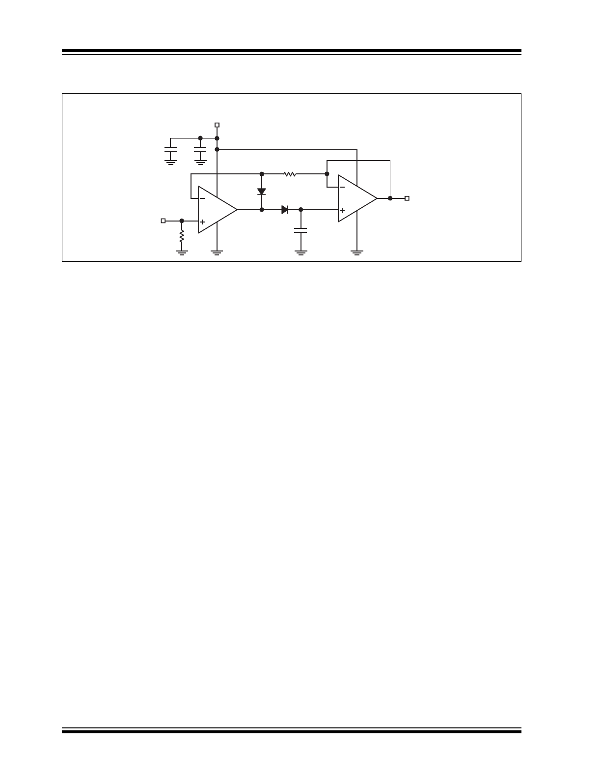
Typical Application Schematic
0.1μF
10μF
100pF
1
/
2
MIC862
1
/
2
MIC862
V
OUT
V+
RF
P
EAK
D
ETECTOR
C
IRCUIT
FOR
AM R
ADIO

2017 Microchip Technology Inc.
DS20005836A-page 3
MIC862
1.0
ELECTRICAL CHARACTERISTICS
Absolute Maximum Ratings †
Supply Voltage (V
V+
to V
V–
).....................................................................................................................................+6.0V
Differential Input Voltage (V
IN+
to V
IN–
) (
Note 1
)......................................................................................................+6.0V
Input Voltage (V
IN+
to V
IN–
) ...........................................................................................................V
V+
+ 0.3V, V
V–
– 0.3V
Output Short-Circuit Current Duration.................................................................................................................Indefinite
ESD Rating (
Note 2
) .................................................................................................................................. ESD Sensitive
Operating Ratings ‡
Supply Voltage (V+ to V-)........................................................................................................................ +2.0V to +5.25V
†
Notice: Stresses above those listed under “Absolute Maximum Ratings” may cause permanent damage to the device.
This is a stress rating only and functional operation of the device at those or any other conditions above those indicated
in the operational sections of this specification is not intended. Exposure to maximum rating conditions for extended
periods may affect device reliability.
‡ Notice:
The device is not guaranteed to function outside the operating ratings.
Note 1:
Exceeding the maximum differential input voltage will damage the input stage and degrade performance (in
particular, input bias current is likely to increase).
2:
Devices are ESD sensitive. Handling precautions are recommended. Human body model, 1.5 kΩ in series
with 100 pF.
MIC862
DS20005836A-page 4
2017 Microchip Technology Inc.
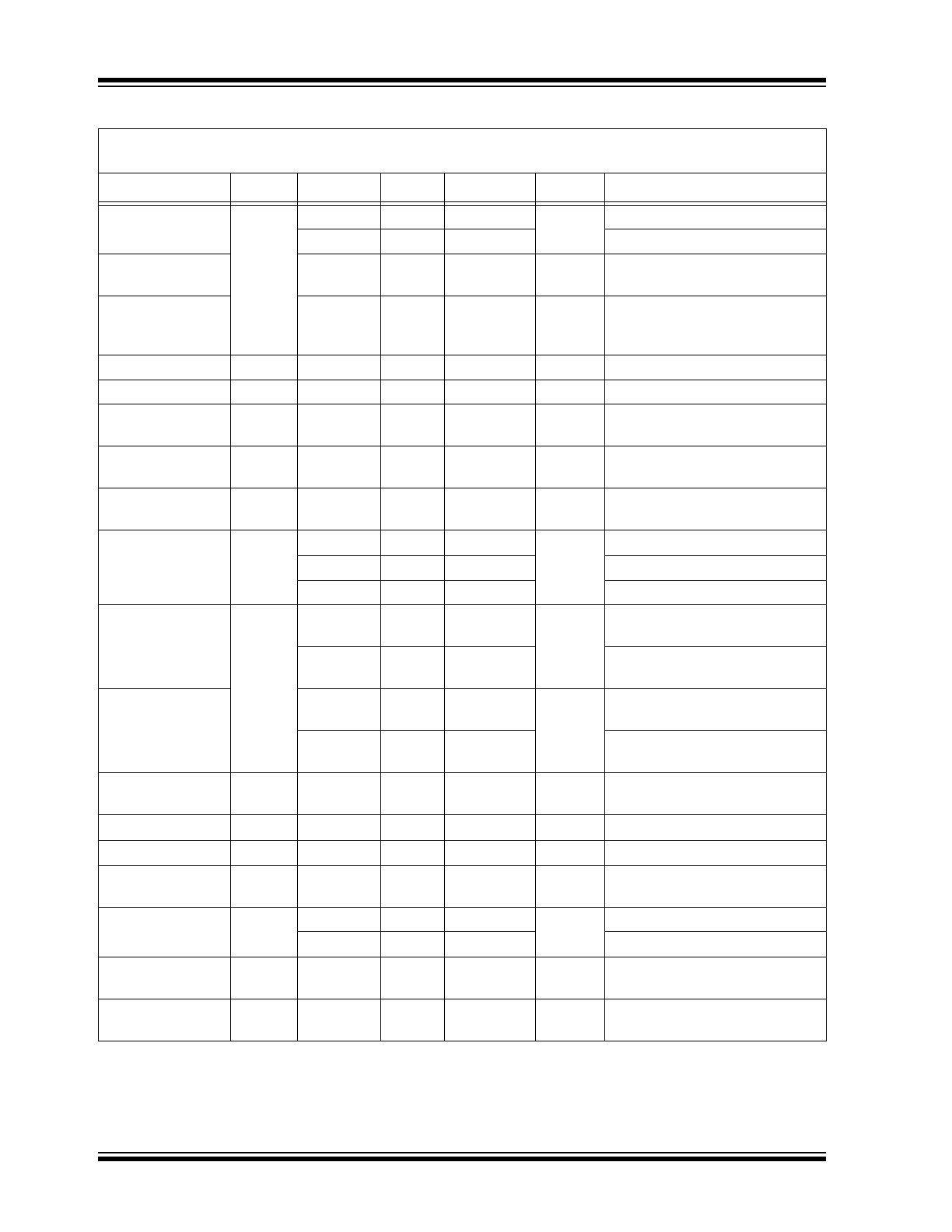
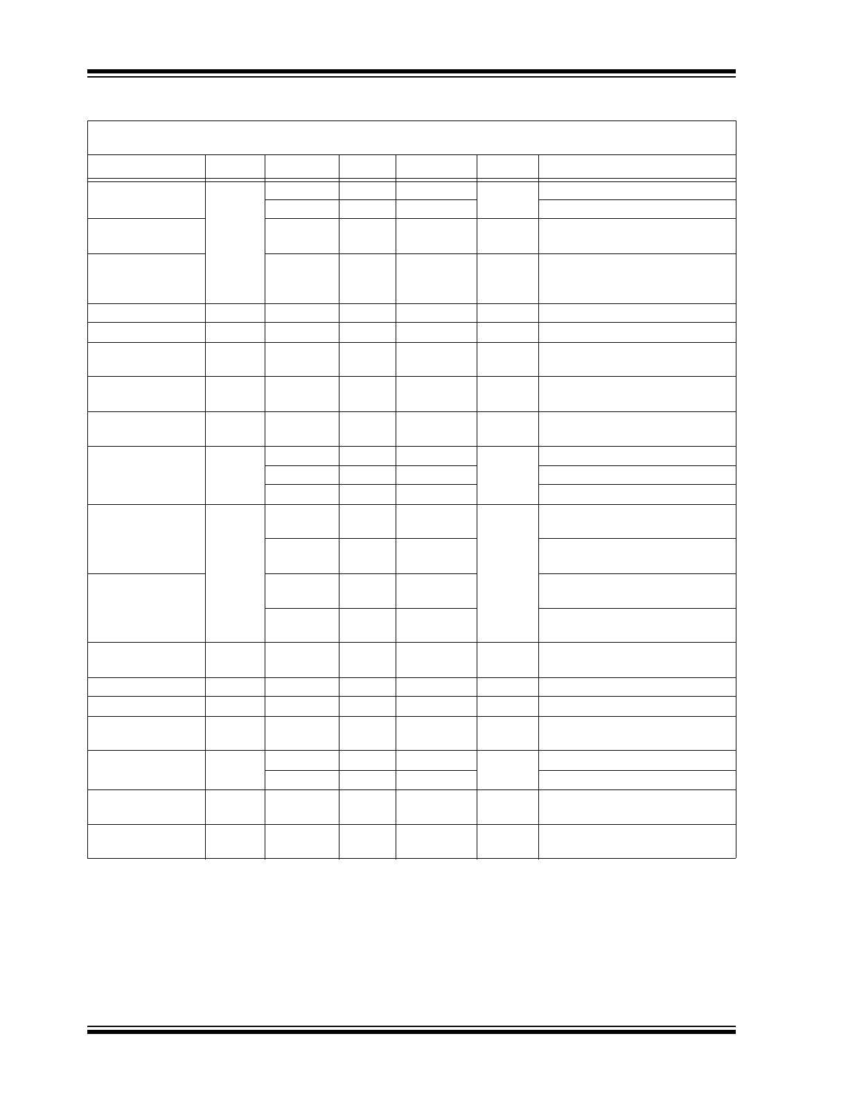
TABLE 1-1:
ELECTRICAL CHARACTERISTICS
Electrical Characteristics:
V+ = +2V, V– = 0V, V
CM
= V+/2; R
L
= 500 kΩ to V+/2; –40°C ≤ T
A
≤ +85°C unless
otherwise noted.
Parameters
Symbol
Min.
Typ.
Max.
Units
Conditions
Input Offset Voltage
V
OS
–6
0.1
6
mV
—
–5
0.1
5
T
A
= +25°C
Differential Offset
Voltage
—
0.5
—
mV
—
Input Offset Voltage
Temperature
Coefficient
—
6
—
µV/°C
—
Input Bias Current
I
B
—
10
—
pA
—
Input Offset Current
I
OS
—
5
—
pA
—
Input Voltage
Range (from V–)
V
CM
0.5
1
—
V
CMRR > 50 dB
Common-Mode
Rejection Ratio
CMRR
45
75
—
dB
0V < V
CM
< 1V
Power Supply
Rejection Ratio
PSRR
50
78
—
dB
Supply voltage change of 2V to
2.7V.
Large-Signal
Voltage Gain
A
VOL
66
74
—
dB
R
L
= 5 kΩ, V
OUT
= 1.4 V
PP
75
89
—
R
L
= 100 kΩ, V
OUT
= 1.4 V
PP
85
100
—
R
L
= 500 kΩ, V
OUT
= 1.4 V
PP
Maximum Output
Voltage Swing
V
OUT
V+ – 80 mV
V+ –
55 mV
—
V
R
L
= 5 kΩ
V+ – 3 mV
V+ –
1.4 mV
—
R
L
= 500 kΩ
Minimum Output
Voltage Swing
—
V– +
14 mV
V– + 20 mV
V
R
L
= 5 kΩ
—
V– +
0.85 mV
V– + 3 mV
R
L
= 500 kΩ
Gain-Bandwidth
Product
GBW
—
2.1
—
MHz
R
L
= 20 kΩ, C
L
= 2 pF, A
V
= 11
Phase Margin
PM
—
57
—
°
R
L
= 20 kΩ, C
L
= 2 pF, A
V
= 11
–3 dB Bandwidth
BW
—
4.2
—
MHz
R
L
= 1 MΩ, C
L
= 2 pF, A
V
= 1
Slew Rate
SR
—
2
—
V/µs
R
L
= 1 MΩ, C
L
= 2 pF, A
V
= 1,
Positive Slew Rate = 1.5 V/µs
Short-Circuit Output
Current
I
SC
1.8
2.6
—
mA
Source
1.5
2.2
—
Sink
Supply Current (per
Op Amp)
I
S
—
27
43
µA
No Load
Channel-to-
Channel Crosstalk
—
—
–100
—
dB
Note 1
Note 1:
DC signal referenced to input. Refer to the
Typical Performance Curves
section’s AC performance graphs.
2017 Microchip Technology Inc.
DS20005836A-page 5
MIC862
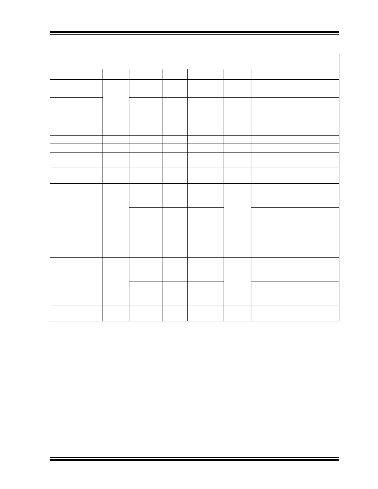
TABLE 1-2:
ELECTRICAL CHARACTERISTICS
Electrical Characteristics:
V+ = +2.7V, V– = 0V, V
CM
= V+/2; R
L
= 500 kΩ to V+/2; –40°C ≤ T
A
≤ +85°C unless
otherwise noted.
Parameters
Symbol
Min.
Typ.
Max.
Units
Conditions
Input Offset Voltage
V
OS
–6
0.1
6
mV
—
–5
0.1
5
T
A
= +25°C
Differential Offset
Voltage
—
0.5
—
mV
—
Input Offset Voltage
Temperature
Coefficient
—
6
—
µV/°C
—
Input Bias Current
I
B
—
10
—
pA
—
Input Offset Current
I
OS
—
5
—
pA
—
Input Voltage
Range (from V–)
V
CM
1
1.8
—
V
CMRR > 60 dB
Common-Mode
Rejection Ratio
CMRR
65
83
—
dB
0V < V
CM
< 1.35V
Power Supply
Rejection Ratio
PSRR
60
85
—
dB
Supply voltage change of 2.7V to
3V
Large-Signal
Voltage Gain
A
VOL
65
77
—
dB
R
L
= 5 kΩ, V
OUT
= 2 V
PP
80
90
—
R
L
= 100 kΩ, V
OUT
= 2 V
PP
90
101
—
R
L
= 500 kΩ, V
OUT
= 2 V
PP
Gain-Bandwidth
Product
GBW
—
2.3
—
MHz
R
L
= 20 kΩ, C
L
= 2 pF, A
V
= 11
Phase Margin
PM
—
50
—
°
R
L
= 20 kΩ, C
L
= 2 pF, A
V
= 11
–3 dB Bandwidth
BW
—
4.2
—
MHz
R
L
= 1 MΩ, C
L
= 2 pF, A
V
= 1
Slew Rate
SR
—
3
—
V/µs
R
L
= 1 MΩ, C
L
= 2 pF, A
V
= 1,
Positive Slew Rate = 1.5 V/µs
Short-Circuit Output
Current
I
SC
4.5
6.3
—
mA
Source
4.5
6.2
—
Sink
Supply Current (per
Op Amp)
I
S
—
28
45
µA
No Load
Channel-to-
Channel Crosstalk
—
—
–120
—
dB
Note 1
Note 1:
DC signal referenced to input. Refer to the
Typical Performance Curves
section’s AC performance graphs.
MIC862
DS20005836A-page 6
2017 Microchip Technology Inc.
TABLE 1-3:
ELECTRICAL CHARACTERISTICS
Electrical Characteristics:
V+ = +5V, V– = 0V, V
CM
= V+/2; R
L
= 500 kΩ to V+/2; –40°C ≤ T
A
≤ +85°C unless
otherwise noted.
Parameters
Symbol
Min.
Typ.
Max.
Units
Conditions
Input Offset Voltage
V
OS
–6
0.1
6
mV
—
–5
0.1
5
T
A
= +25°C
Differential Offset
Voltage
—
0.5
—
mV
—
Input Offset Voltage
Temperature
Coefficient
—
6
—
µV/°C
—
Input Bias Current
I
B
—
10
—
pA
—
Input Offset Current
I
OS
—
5
—
pA
—
Input Voltage
Range (from V–)
V
CM
3.5
4.1
—
V
CMRR > 60 dB
Common-Mode
Rejection Ratio
CMRR
60
87
—
dB
0V < V
CM
< 3.5V
Power Supply
Rejection Ratio
PSRR
60
92
—
dB
Supply voltage change of
3V to 5V
Large-Signal
Voltage Range
A
VOL
65
73
—
dB
R
L
= 5 kΩ, V
OUT
= 4.8 V
PP
80
86
—
R
L
= 100 kΩ, V
OUT
= 4.8 V
PP
89
96
—
R
L
= 500 kΩ, V
OUT
= 4.8 V
PP
Maximum Output
Voltage Swing
V
OUT
V+ – 50 mV
V+ –
37 mV
—
V
R
L
= 5 kΩ
V+ – 3 mV
V+ –
1.3 mV
—
R
L
= 500 kΩ
Minimum Output
Voltage Swing
—
V– +
24 mV
V– + 40 mV
R
L
= 5 kΩ
—
V– +
0.7 mV
V– + 3 mV
R
L
= 500 kΩ
Gain-Bandwidth
Product
GBW
—
3
—
MHz
R
L
= 20 kΩ, C
L
= 2 pF, A
V
= 11
Phase Margin
PM
—
45
—
°
—
–3 dB Bandwidth
BW
—
5
—
MHz
R
L
= 1 MΩ, C
L
= 2 pF, A
V
= 1
Slew Rate
SR
—
4
—
V/µs
R
L
= 1 MΩ, C
L
= 2 pF, A
V
= 1,
Positive Slew Rate = 1.5 V/µs
Short-Circuit Output
Current
I
SC
17
23
—
mA
Source
18
27
—
Sink
Supply Current (per
Op Amp)
I
S
—
31
47
µA
No Load
Channel-to-
Channel Crosstalk
—
—
–120
—
dB
Note 1
Note 1:
DC signal referenced to input. Refer to the
Typical Performance Curves
section’s AC performance graphs.
2017 Microchip Technology Inc.
DS20005836A-page 7
MIC862
TEMPERATURE SPECIFICATIONS (
Note 1
)
Parameters
Sym.
Min.
Typ.
Max.
Units
Conditions
Temperature Ranges
Operating Temperature Range
—
–40
—
+125
°C
—
Storage Temperature Range
T
S
—
—
+150
°C
—
Ambient Temperature Range
T
A
–40
—
+85
°C
—
Package Thermal Resistance
Thermal Resistance SOT-23-8
JA
—
100
—
°C/W
Using 4-Layer PCB
JC
—
70
—
°C/W
Using 4-Layer PCB
Note 1:
The maximum allowable power dissipation is a function of ambient temperature, the maximum allowable
junction temperature and the thermal resistance from junction to air (i.e., T
A
, T
J
,
JA
). Exceeding the
maximum allowable power dissipation will cause the device operating junction temperature to exceed the
maximum +125°C rating. Sustained junction temperatures above +125°C can impact the device reliability.
MIC862
DS20005836A-page 8
2017 Microchip Technology Inc.
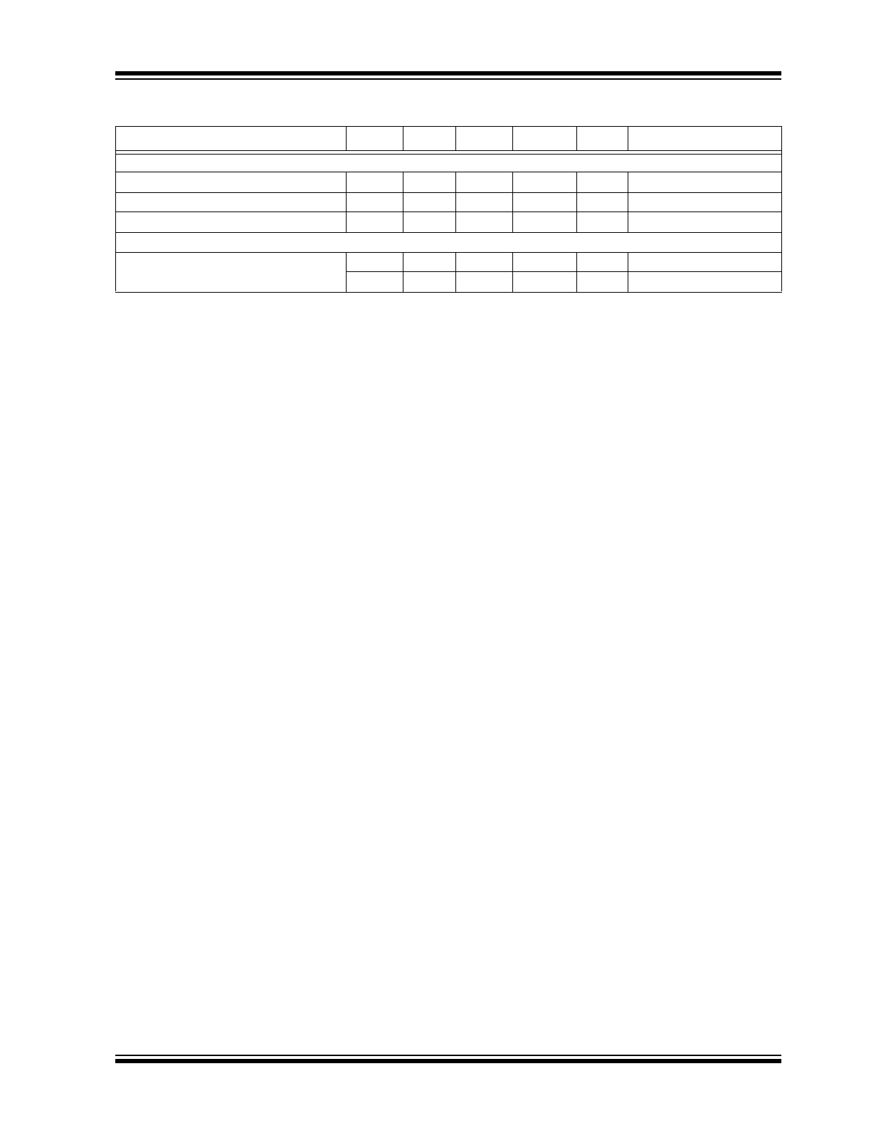
2.0
TYPICAL PERFORMANCE CURVES
FIGURE 2-1:
Short-Circuit Current vs.
Supply Voltage.
FIGURE 2-2:
Output Voltage vs. Output
Current.
FIGURE 2-3:
Output Voltage vs. Output
Current.
FIGURE 2-4:
Short-Circuit Current vs.
Supply Voltage.
FIGURE 2-5:
Output Voltage vs. Output
Current.
FIGURE 2-6:
Output Voltage vs. Output
Current.
Note:
The graphs and tables provided following this note are a statistical summary based on a limited number of
samples and are provided for informational purposes only. The performance characteristics listed herein
are not tested or guaranteed. In some graphs or tables, the data presented may be outside the specified
operating range (e.g., outside specified power supply range) and therefore outside the warranted range.
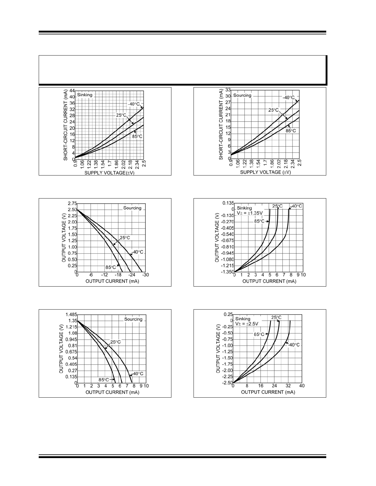
2017 Microchip Technology Inc.
DS20005836A-page 9
MIC862
FIGURE 2-7:
Supply Current vs. Supply
Voltage.
FIGURE 2-8:
Offset Voltage vs.
Temperature.
FIGURE 2-9:
Offset Voltage vs.
Common-Mode Voltage.
FIGURE 2-10:
Offset Voltage vs.
Common-Mode Voltage.
FIGURE 2-11:
Short-Circuit Current vs.
Temperature.
FIGURE 2-12:
Short-Circuit Current. vs.
Temperature.
MIC862
DS20005836A-page 10
2017 Microchip Technology Inc.
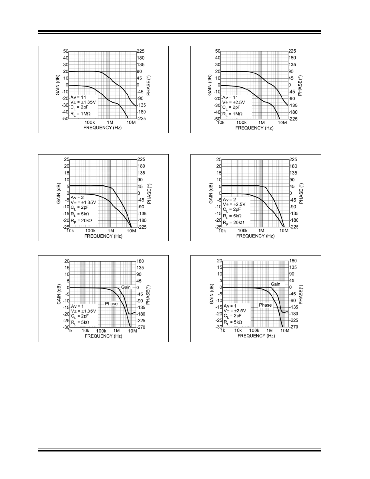
FIGURE 2-13:
Gain Bandwidth and Phase
Margin.
FIGURE 2-14:
Gain Frequency Response.
FIGURE 2-15:
Unity Gain Frequency
Response.
FIGURE 2-16:
Gain Bandwidth and Phase
Margin.
FIGURE 2-17:
Gain Frequency Response.
FIGURE 2-18:
Unity Gain Frequency
Response.