
2017 Microchip Technology Inc.
DS20005774A-page 1
MIC5212
Features
• Fused-Lead Frame SOIC-8
• Up to 500 mA per Regulator Output
• Low Quiescent Current
• Low Dropout Voltage
• Tight Load and Line Regulation
• Low Temperature Coefficient
• Current and Thermal Limiting
• Reversed Input Polarity Protection
Applications
• Hard Disk Drives
• CD R/W
• Barcode Scanners
• SMPS Post Regulator and DC/DC Modules
• High-Efficiency Linear Power Supplies
General Description
The MIC5212 is a dual linear voltage regulator with
very low dropout voltage (typically 10 mV at light loads
and 350 mV at 500 mA), very low ground current
(225 μA at 10 mA output), and better than 1% initial
accuracy.
Both regulator outputs can supply up to 500 mA at the
same time as long as each regulator’s maximum
junction temperature is not exceeded.
Key features include current limiting, overtemperature
shutdown, and protection against reversed battery.
The MIC5212 is available in a fixed 3.3V/2.5V output
voltage configuration. Other voltages are available;
contact Microchip for details.
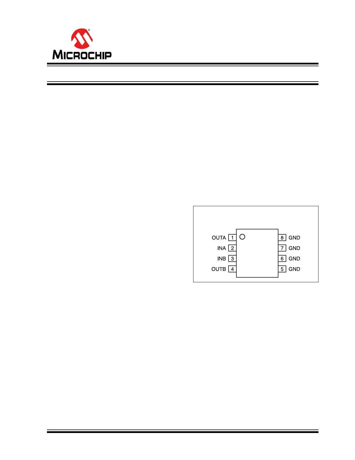
Package Type
MIC5212
SOIC-8
Top View
Dual 500 mA LDO Regulator
MIC5212
DS20005774A-page 2
2017 Microchip Technology Inc.
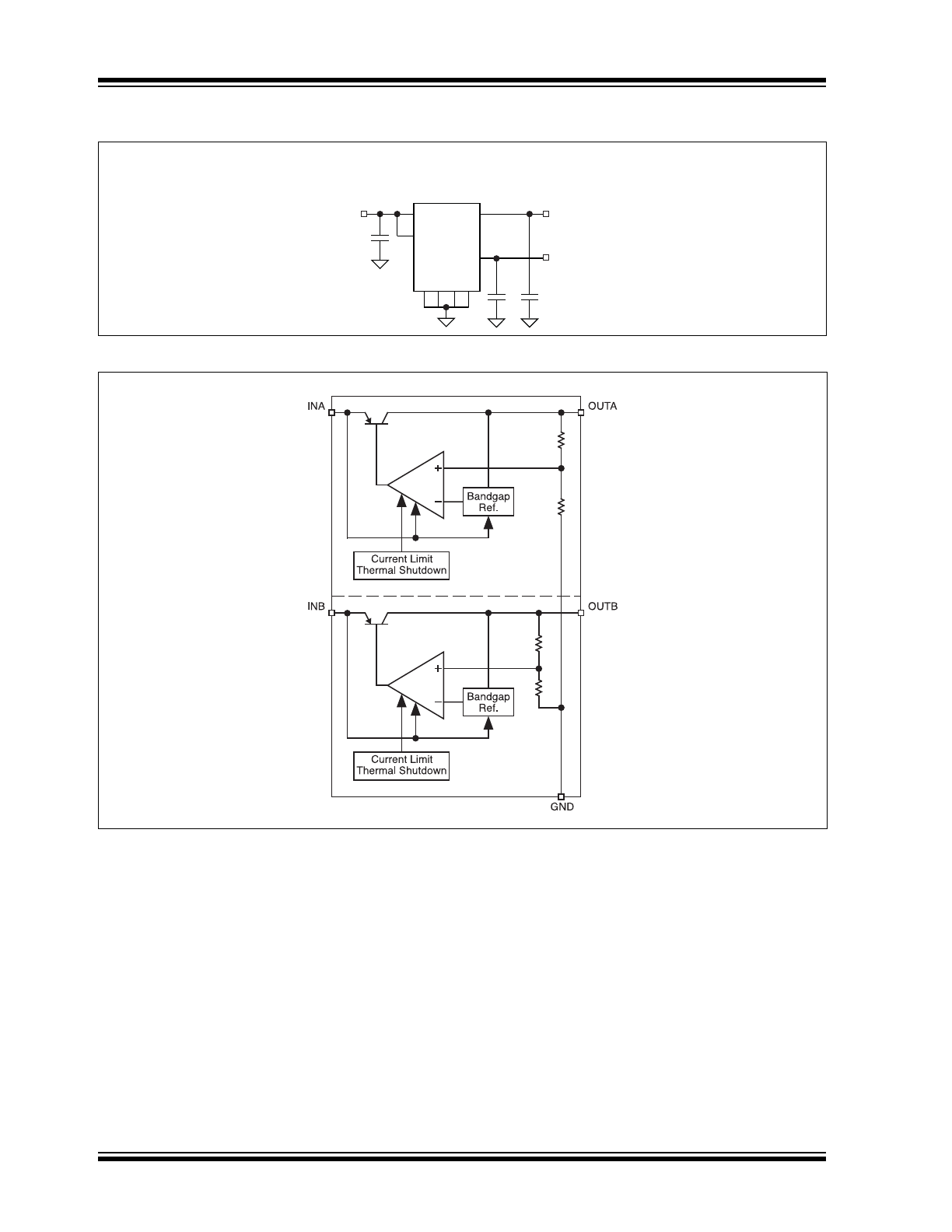
Typical Application Circuit
Functional Diagram
MIC5212
3.3V/2.5V Dual LDO
V
O1
= 3.3V
V
O2
= 2.5V
IN = 5V
4.7
µF
4.7
µF 4.7µF
MIC5212-SJYM
GND
OUTB
OUTA
INA
INB
2017 Microchip Technology Inc.
DS20005774A-page 3
MIC5212
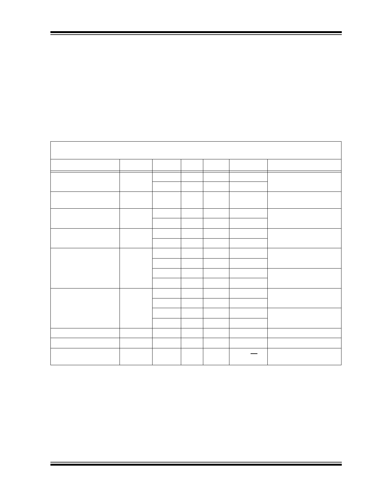
1.0
ELECTRICAL CHARACTERISTICS
Absolute Maximum Ratings †
Supply Input Voltage, (V
IN
A or B) .............................................................................................................. –20V to +20V
Power Dissipation ................................................................................................................................. Internally Limited
Operating Ratings ††
Supply Input Voltage, (V
IN
) ....................................................................................................................... +2.5V to +16V
†
Notice: Exceeding the absolute maximum rating may damage the device.
††
Notice: The device is not guaranteed to function outside its operating rating.
DC CHARACTERISTICS
Electrical Characteristics:
Unless otherwise indicated, Regulator A and B V
IN
= V
OUT
+ 1V; I
L
= 100 μA;
C
L
= 4.7 μF; T
J
= +25°C, bold values indicate –40°C ≤ T
J
≤ +125°C.
Parameters
Symbol
Min.
Typ.
Max.
Units
Conditions
Output Voltage Accuracy
V
O
–1
—
1
%
Variation from specified
V
OUT
–2
—
2
%
Output Voltage
Temperature Coefficient
∆V
O
/∆T
—
40
—
ppm/°C
Note 1
Line Regulation
∆V
O
/V
O
—
0.009
0.05
%/V
V
IN
= V
OUT
+ 1V to 16V
—
—
0.1
%/V
Load Regulation
∆V
O
/V
O
—
0.05
0.7
%
I
L
= 0.1 mA to 500 mA,
Note 2
—
—
1
%
Dropout Voltage,
Note 3
(per regulator)
V
IN
– V
O
—
175
275
mV
I
L
= 150 mA
—
—
350
mV
—
350
500
mV
I
L
= 150 mA
—
—
600
mV
Ground Pin Current,
Note 4
(per regulator)
I
GND
—
1.5
2.5
mA
I
L
= 150 mA
—
—
3.0
mA
—
12
20
mA
I
L
= 150 mA
—
—
25
mA
Ripple Rejection
PSRR
—
75
—
dB
f = 120 Hz, I
L
= 150 mA
Current Limit
I
LIMIT
—
750
1000
mA
V
OUT
= 0V
Spectral Noise Density
—
—
500
—
nV/√Hz
V
OUT
= 2.5V, I
OUT
= 50 mA,
C
OUT
= 2.2 μF
Note 1:
Output voltage temperature coefficient is defined as the worst case voltage change divided by the total
temperature range.
2:
Regulation is measured at constant junction temperature using low duty cycle pulse testing. Parts are
tested for load regulation in the load range from 0.1 mA to 500 mA. Changes in output voltage due to
heating effects are covered by the thermal regulation specification.
3:
Dropout voltage is defined as the input to output differential at which the output voltage drops 2% below its
nominal value measured at 1V differential.
4:
Ground pin current is the regulator quiescent current plus pass transistor base current. The total current
drawn from the supply is the sum of the load current plus the ground pin current.
MIC5212
DS20005774A-page 4
2017 Microchip Technology Inc.
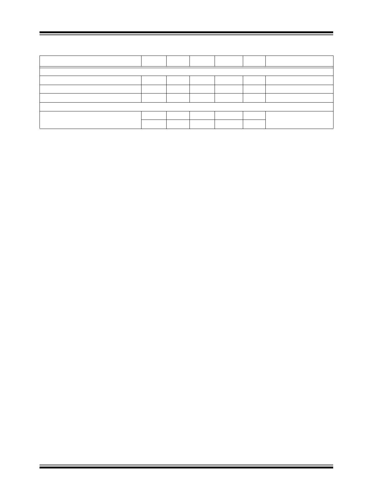
TEMPERATURE SPECIFICATIONS (
Note 1
)
Parameters
Sym.
Min.
Typ.
Max.
Units
Conditions
Temperature Ranges
Storage Temperature Range
T
A
–60
—
+150
°C
—
Lead Temperature
T
J
—
+260
—
°C
Soldering, 5 sec.
Junction Temperature
T
J
–40
—
+125
°C
—
Package Thermal Resistances
Thermal Resistance, SOIC-8Ld
JC
—
20
—
°C/W
Note 2
JA
—
63
—
°C/W
Note 1:
The maximum allowable power dissipation is a function of ambient temperature, the maximum allowable
junction temperature and the thermal resistance from junction to air (i.e., T
A
, T
J
,
JA
). Exceeding the
maximum allowable power dissipation will cause the device operating junction temperature to exceed the
maximum +125°C rating. Sustained junction temperatures above +125°C can impact the device reliability.
2:
Absolute maximum ratings indicate limits beyond which damage to the component may occur. Electrical
specifications do not apply when operating the device outside of its operating ratings. The maximum
allowable power dissipation is a function of the maximum junction temperature, T
J(max)
, the junc-
tion-to-ambient thermal resistance, θ
JA
, and the ambient temperature, T
A
. The maximum allowable power
dissipation at any ambient temperature is calculated using: P
D(max)
= (T
J(max)
– T
A
) ÷ θ
JA
. Exceeding the
maximum allowable power dissipation will result in excessive die temperature, and the regulator will go
into thermal shutdown. The θ
JA
of the 8-lead SOIC (M) is 63°C/W mounted on a PC board.
2017 Microchip Technology Inc.
DS20005774A-page 5
MIC5212
2.0
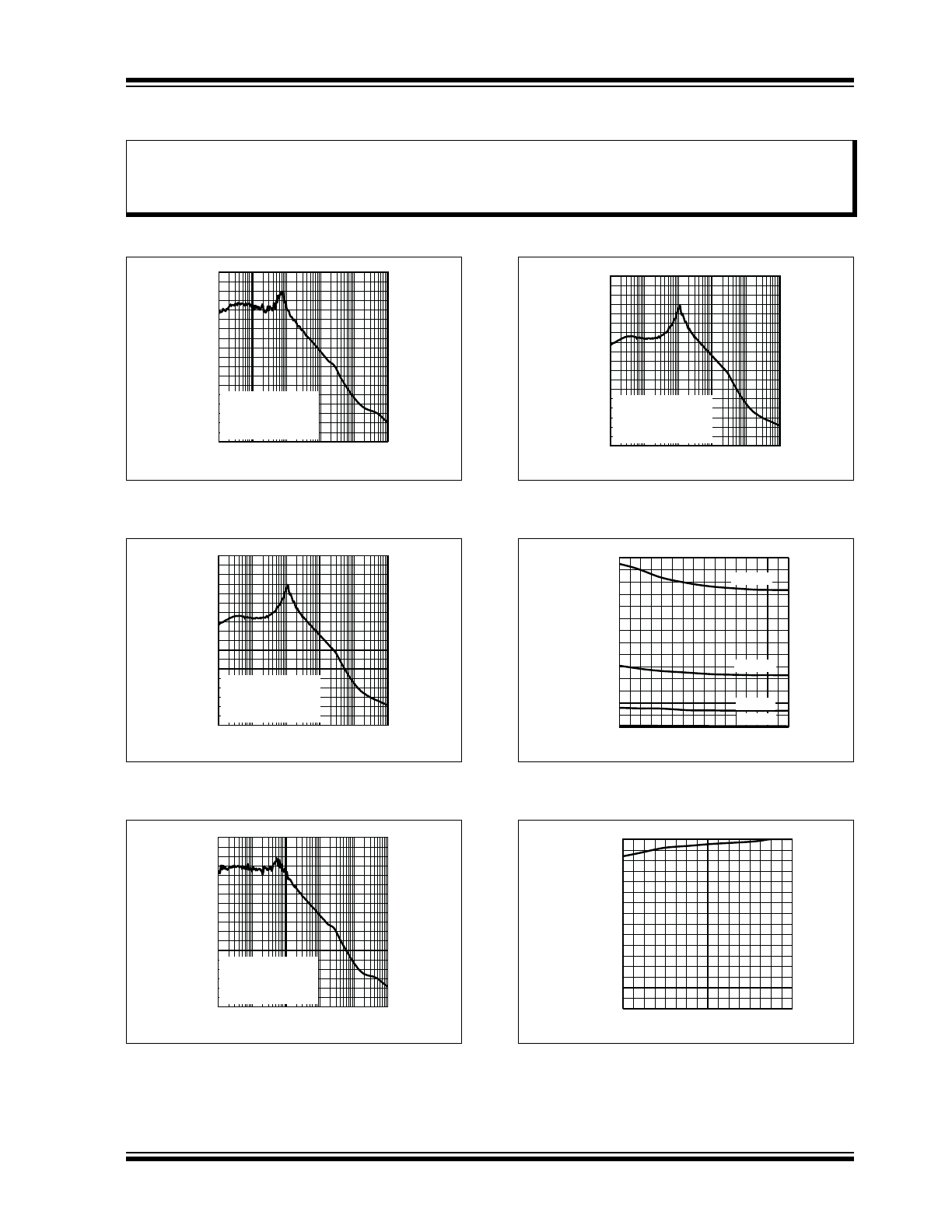
TYPICAL PERFORMANCE CURVES
FIGURE 2-1:
MIC5212-3.3 PSRR 150 mA
Load.
FIGURE 2-2:
MIC5212-3.3 PSRR 500 mA
Load.
FIGURE 2-3:
MIC5212-2.5 PSRR 150 mA
Load.
FIGURE 2-4:
MIC5212-2.5 PSRR 500 mA
Load.
FIGURE 2-5:
Ground Current vs.
Temperature.
FIGURE 2-6:
Short Circuit Current vs.
Temperature.
Note:
The graphs and tables provided following this note are a statistical summary based on a limited number of
samples and are provided for informational purposes only. The performance characteristics listed herein
are not tested or guaranteed. In some graphs or tables, the data presented may be outside the specified
operating range (e.g., outside specified power supply range) and therefore outside the warranted range.
0
10
20
30
40
50
60
70
80
90
PSRR (dB)
FREQUENCY (Hz)
C
OUT
= 10
μF Tantulum
V
IN
= 4.3V
V
OUT
= 3.3V
V
IN
= V
OUT
+ 1V
10
100
1k
10k
100k
1M
0
10
20
30
40
50
60
70
80
90
PSRR (dB)
FREQUENCY (Hz)
C
OUT
= 10
μF Tantulum
V
IN
= 4.3V
V
OUT
= 3.3V
V
IN
= V
OUT
+ 1V
10
100
1k
10k
100k
1M
0
10
20
30
40
50
60
70
80
90
PSRR (dB)
FREQUENCY (Hz)
C
OUT
= 10
μF Tantulum
V
IN
= 4.3V
V
OUT
= 3.3V
V
IN
= V
OUT
+ 1V
10
100
1k
10k
100k
1M
0
10
20
30
40
50
60
70
80
90
PSRR (dB)
FREQUENCY (Hz)
C
OUT
= 10
μF Tantulum
V
IN
= 4.3V
V
OUT
= 3.3V
V
IN
= V
OUT
+ 1V
10
100
1k
10k
100k
1M
0
2
4
6
8
10
12
14
-40 -20 0
20 40 60 80 100 120
GROUND CURRENT (mA)
TEMPERATURE (
°C)
500mA
150mA
100
μA
300mA
0
100
200
300
400
500
600
700
800
-40 -20 0
20 40 60 80 100 120
LOAD CURRENT (mA)
TEMPERATURE (
°C)
MIC5212
DS20005774A-page 6
2017 Microchip Technology Inc.
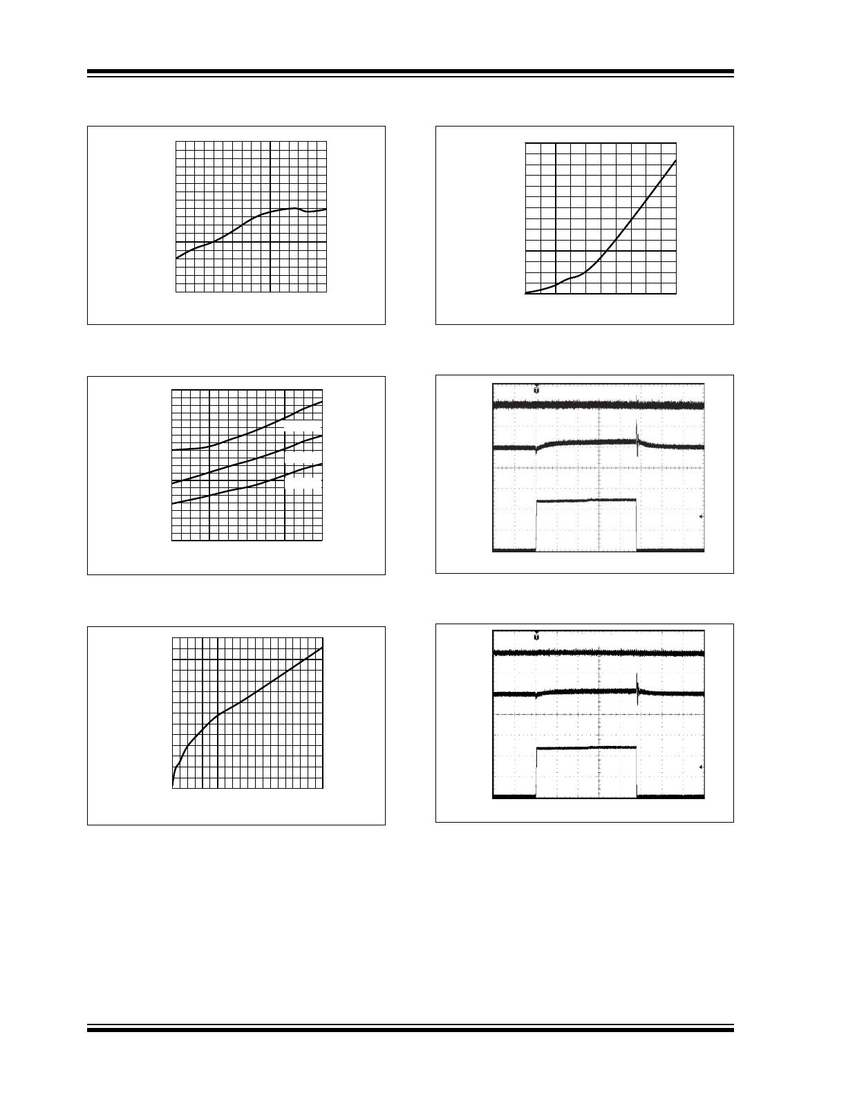
FIGURE 2-7:
Output Voltage vs.
Temperature.
FIGURE 2-8:
Dropout Voltage vs.
Temperature.
FIGURE 2-9:
Dropout Voltage vs. Load
Current.
.
FIGURE 2-10:
Ground Current vs. Load
Current.
FIGURE 2-11:
Output 1 Load Transient
Response.
FIGURE 2-12:
Output 2 Load Transient
Response.
3.275
3.280
3.285
3.290
3.295
3.300
3.305
3.310
3.315
3.320
-40 -20 0
20 40 60 80 100 120
OUTPUT VOLTAGE (V)
TEMPERATURE (
°C)
0
50
100
150
200
250
300
350
400
450
500
-40 -20 0
20 40 60 80 100 120
DROPOUT VOLTAGE (mV)
TEMPERATURE (
°C)
500mA
150mA
300mA
0
50
100
150
200
250
300
350
0
50
100
150
200
250
300
350
400
450
500
DROPOUT VOLTAGE (mV)
OUTPUT CURRENT (mA)
0
2
4
6
8
10
12
14
0
100
200
300
400
500
GROUND CURRENT (mA)
OUTPUT CURRENT (mA)
TIME (1ms/div.)
OUTPUT
CURRENT
(500mA/div)
OUTPUT
2
(20mV/div)
OUTPUT
1
(20mV/div)
V
IN
= 3.3V
V
OUT
= 2.5V
C
OUT
= 10 F Ceramic
1000mA
10mA
500mA
10mA
TIME (1ms/div.)
OUTPUT
2 CURRENT
(200mA/div)
OUTPUT
1
(20mV/div)
OUTPUT
2
(20mV/div)
V
IN
= 3.3V
V
OUT
= 2.5V
C
OUT
= 10 F Ceramic
1000mA
10mA
500mA
10mA
2017 Microchip Technology Inc.
DS20005774A-page 7
MIC5212
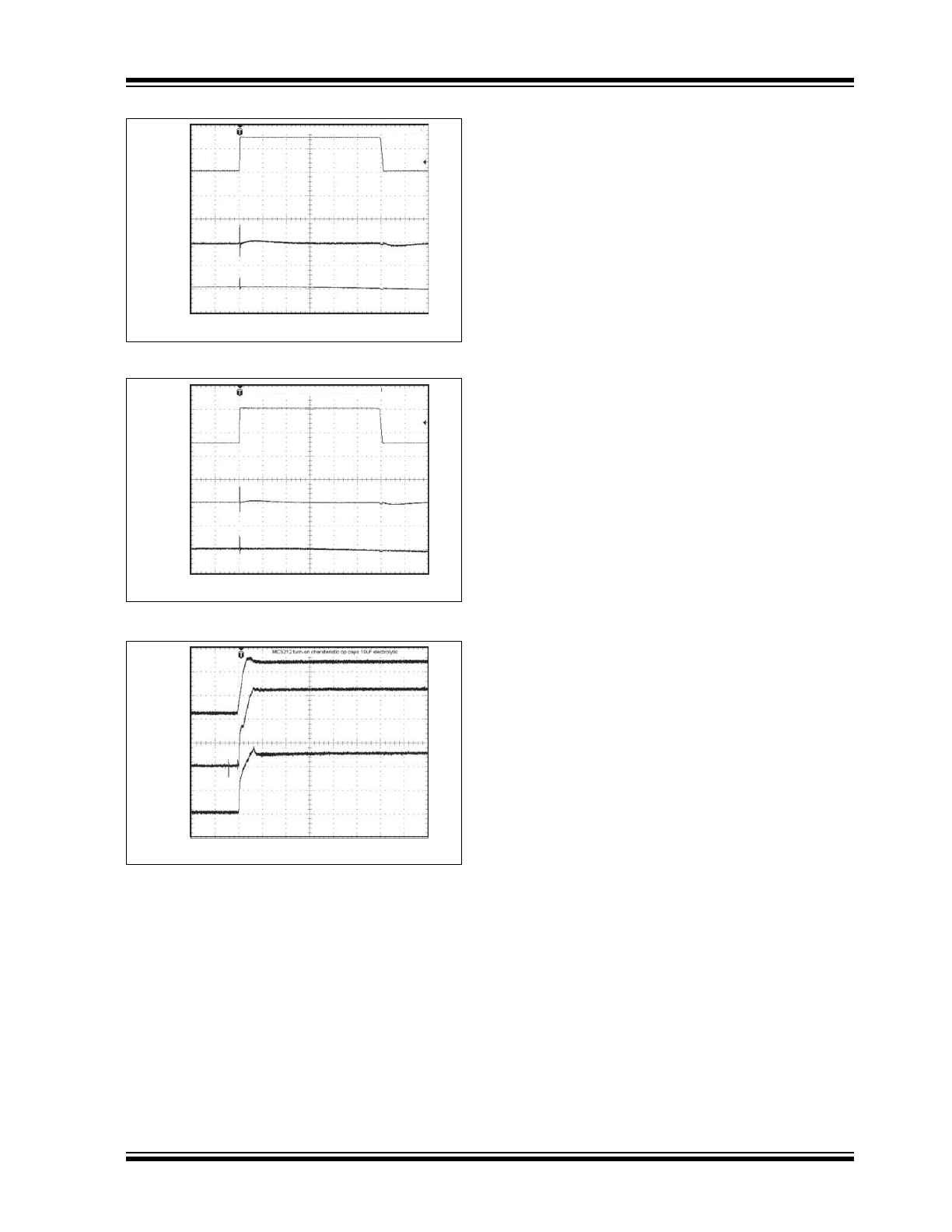
FIGURE 2-13:
Line Transient Response.
FIGURE 2-14:
Line Transient Response.
FIGURE 2-15:
Turn-On Response.
TIME (1ms/div.)
VOUT
1
(10mV/div)
VOUT
2
(10mV/div)
VIN
(2V/div)
V
IN
= 3.3V
V
OUT
= 2.5V
C
OUT
= 10 F Ceramic
1000mA
10mA
4.3V
7V
TIME (1ms/div.)
VOUT
1
(10mV/div)
VOUT
2
(10mV/div)
VIN
(2V/div)
6V
3.5V
TIME (40
μs/div.)
OUTPUT
2
(1V/div)
OUTPUT
1
(1V/div)
VSUPPL
Y
(2V/div)
3.3V, 500mA
2.5V, 200mA
MIC5212
DS20005774A-page 8
2017 Microchip Technology Inc.
3.0
PIN DESCRIPTIONS
The descriptions of the pins are listed in
Table 3-1
.
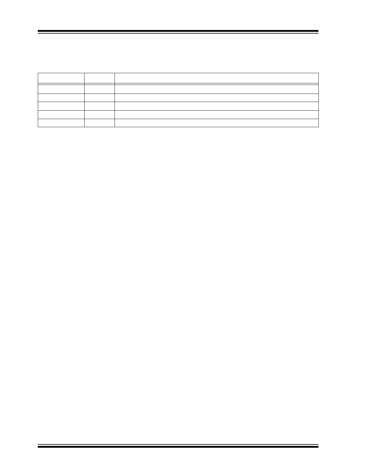
TABLE 3-1:
PIN FUNCTION TABLE
Pin Number
Pin Name
Description
1
OUTA
Regulator A Output.
2
INA
Regulator A Input.
3
INB
Regulator B Input.
4
OUTB
Regulator B Output.
5, 6, 7, 8
GND
Ground.
2017 Microchip Technology Inc.
DS20005774A-page 9
MIC5212
4.0
DEVICE OVERVIEW
4.1
Input Capacitor
A 1 μF capacitor should be placed from IN to GND if
there is more than 10 inches of wire between the input
and the AC filter capacitor or if a battery is used as the
input.
4.2
Output Capacitor
An output capacitor is required between OUT and GND
to prevent oscillation. 1.0 μF minimum is
recommended. Larger values improve the regulator’s
transient response. The output capacitor value may be
increased without limit.
The output capacitor should have an ESR (Effective
Series Resistance) of about 5Ω or less and a resonant
frequency above 1 MHz. Ultra-low-ESR capacitors
may cause a low-amplitude oscillation and/or
underdamped transient response. Most tantalum or
aluminum electrolytic capacitors are adequate; film
types will work, but are more expensive. Since many
aluminum electrolytic capacitors have electrolytes that
freeze at about –30°C, solid tantalum capacitors are
recommended for operation below –25°C.
At lower values of output current, less output
capacitance is required for output stability. The
capacitor can be reduced to 0.47 μF for current below
10 mA or 0.33 μF for currents below 1 mA.
4.3
No-Load Stability
The MIC5212 will remain stable and in regulation with
no load (other than the internal voltage divider) unlike
many other voltage regulators. This is especially
important in CMOS RAM keep-alive applications.
4.4
Dual-Supply Operation
When used in dual supply systems where the regulator
load is returned to a negative supply, the output voltage
must be diode clamped to ground.
4.4.1
POWER SO-8 THERMAL
CHARACTERISTICS
One of the secrets of the MIC5212’s performance is its
power SO-8 package featuring half the thermal
resistance of a standard SO-8 package. Lower thermal
resistance means more output current or higher input
voltage for a given package size.
Lower thermal resistance is achieved by joining the
four ground leads with the die attach paddle to create a
single-unit electrical and thermal conductor. This
concept has been used by MOSFET manufacturers for
years, proving very reliable and cost effective for the
user.
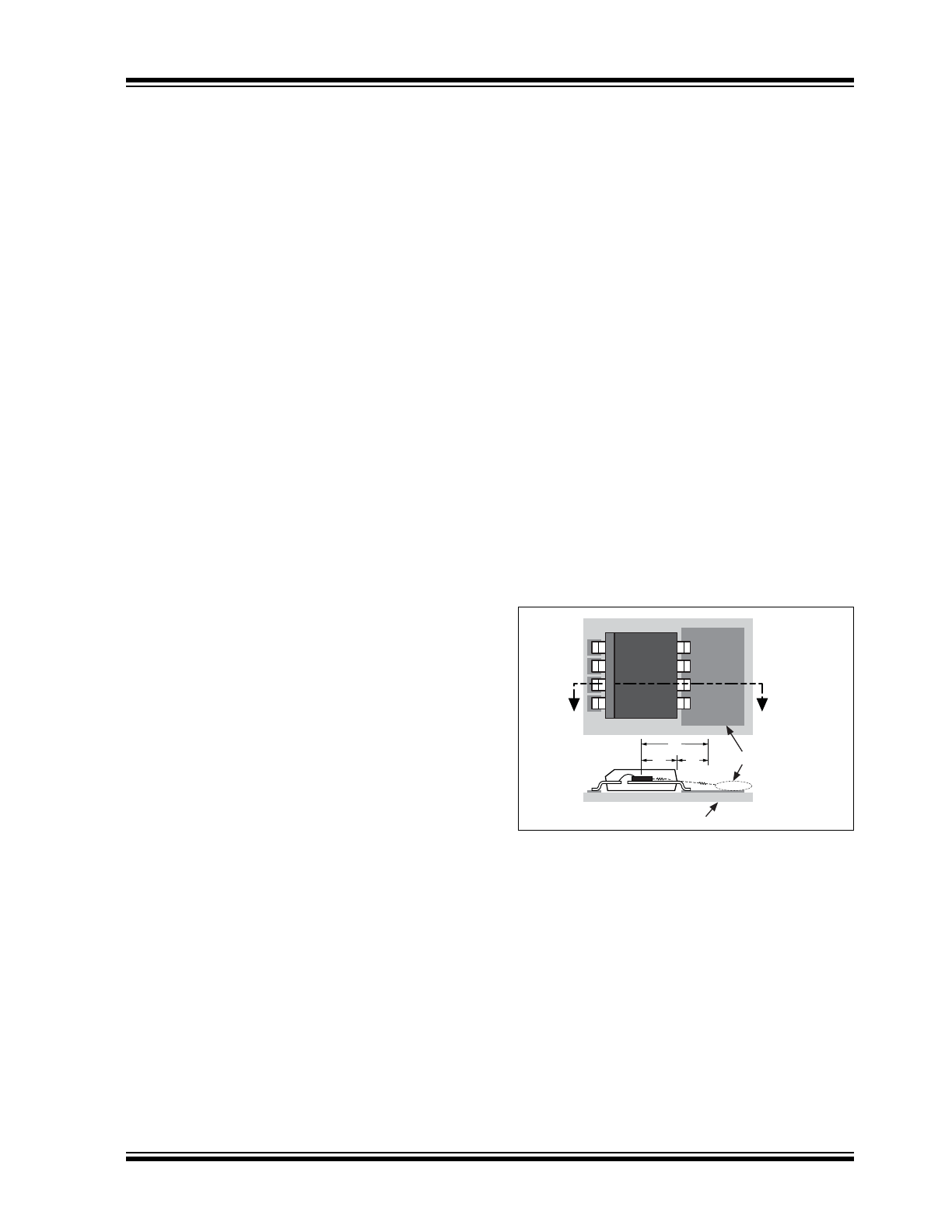
Thermal resistance consists of two main elements, θ
JC
(junction-to-case thermal resistance) and θ
CA
(case-to-ambient thermal resistance). See
Figure 4-1
.
θ
JC
is the resistance from the die to the leads of the
package. θ
CA
is the resistance from the leads to the
ambient air and it includes θ
CS
(case-to-sink thermal
resistance) and θ
SA
(sink-to-ambient thermal
resistance).
FIGURE 4-1:
Thermal Resistance.
Using the power SO-8 reduces the θ
JC
dramatically
and allows the user to reduce θ
CA
. The total thermal
resistance,
θ
JA
(junction-to-ambient thermal
resistance) is the limiting factor in calculating the
maximum power dissipation capability of the device.
Typically, the power SO-8 has a θ
JC
of 20°C/W, this is
significantly lower than the standard SO-8 which is
typically 75°C/W. θ
CA
is reduced because pins 5
through 8 can now be soldered directly to a ground
plane which significantly reduces the case-to-sink
thermal resistance and sink to ambient thermal
resistance.
These low dropout linear regulators are rated to a
maximum junction temperature of 125°C. It is important
not to exceed this maximum junction temperature
θ
JA
θ
JC
θ
CA
printed circuit board
ground plane
heat sink area
SO-8
AMBIENT
MIC5212
DS20005774A-page 10
2017 Microchip Technology Inc.
during operation of the device. To prevent this
maximum junction temperature from being exceeded,
the appropriate ground plane heat sink must be used.
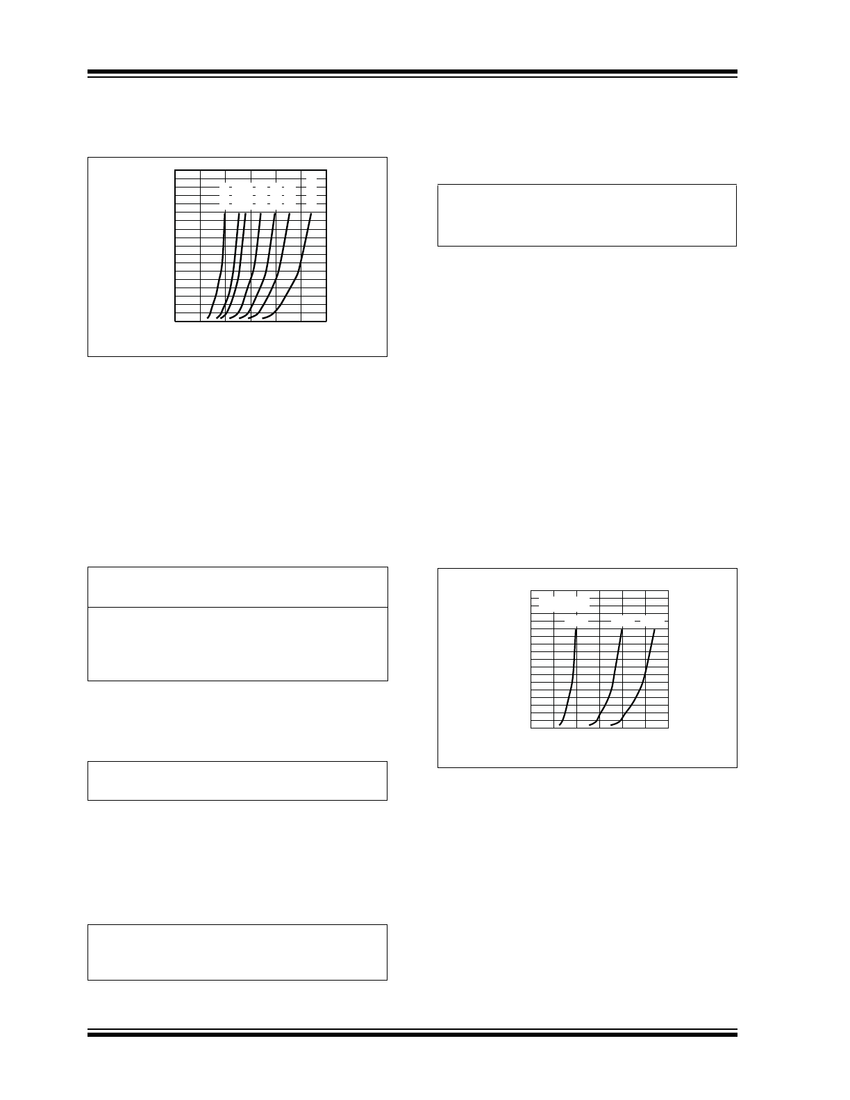
FIGURE 4-2:
Copper Area vs. Power-SO
Power Dissipation (∆T
JA
).
Figure 4-2
shows copper area versus power
dissipation with each trace corresponding to a different
temperature rise above ambient.
From these curves, the minimum area of copper
necessary for the part to operate safely can be
determined. The maximum allowable temperature rise
must be calculated to determine operation along which
curve.
EQUATION 4-1:
For example, the maximum ambient temperature is
50°C, the ∆T is determined as shown in
Equation 4-2
.
EQUATION 4-2:
Using
Figure 4-2
, the minimum amount of required
copper can be determined based on the required
power dissipation.
Power dissipation in a linear regulator is calculated as
shown in
Equation 4-3
.
EQUATION 4-3:
With a common 5V input, a 3.3V, 300 mA output on
LDO 1 and a 2.5V, 150 mA output on LDO 2, power
dissipation is as follows:
EQUATION 4-4:
From
Figure 4-2
, the minimum amount of copper
required to operate this application at a ∆T of 75°C is
500 mm
2
.
4.4.2
QUICK METHOD
Determine the power dissipation requirements for the
design along with the maximum ambient temperature
at which the device will be operated. Refer to
Figure 4-3
, which shows safe operating curves for
three different ambient temperatures: 25°C, 50°C and
85°C. From these curves, the minimum amount of
copper can be determined by knowing the maximum
power dissipation required. If the maximum ambient
temperature is 50°C and the power dissipation is as
above, 920 mW, the curve in
Figure 4-3
shows that the
required area of copper is 500 mm
2
.
The θ
JA
of this package is ideally 63°C/W, but it will
vary depending upon the availability of copper ground
plane to which it is attached.
FIGURE 4-3:
Copper Area vs. Power-SO
Power Dissipation (T
A
).
Where:
T
J(max)
= 125°C
T
A(max)
= Maximum ambient operating
temperature
∆T
=
125°C – 50°C
∆T
=
75°C
0
100
200
300
400
500
600
700
800
900
0
0.25 0.50 0.75 1.00 1.25 1.50
COPPER AREA (mm
2
)
POWER DISSIPATION (W)
40°C
50°C 55°C
65°C
75°C
85°C
100°C
T
T
J max
T
A max
–
=
P
D
V
IN1
V
OUT1
–
I
OUT1
V
IN1
+
I
GND1
V
IN2
V
OUT2
–
+
I
OUT2
V
IIN2
+
I
GND2
=
P
D
=
P
D
=
0.919W
5V
3.3V
–
300mA
5V
+
5mA
5V
2.5V
–
+
150mA
5V
+
1.8mA
0
100
200
300
400
500
600
700
800
900
0
0.25 0.50 0.75 1.00 1.25 1.50
COPPER AREA (mm
2
)
POWER DISSIPATION (W)
85
°C
50
°C 25°C
T
J
= 125
°C