
2000 Microchip Technology Inc.
Preliminary
DS30034B-page 1
PIC16F62X
This document includes the programming
specifications for the following devices:
• PIC16F627
• PIC16F628
• PIC16LF627
• PIC16LF628
1.0
PROGRAMMING THE
PIC16F62X
The PIC16F62X is programmed using a serial method.
The serial mode will allow the PIC16F62X to be pro-
grammed while in the users system. This allows for
increased design flexibility. This programming specifi-
cation applies to PIC16F62X devices in all packages.
PIC16F62X devices may be programmed using a sin-
gle +5 volt supply (low voltage programming mode).
1.1
Hardware Requirements
The PIC16F62X requires one programmable power
supply for V
DD
(4.5V to 5.5V) and a V
PP
of 12V to 14V,
or V
PP
of 4.5V to 5.5V, when using low voltage. Both
supplies should have a minimum resolution of 0.25V.
1.2
Programming Mode
The programming mode for the PIC16F62X allows pro-
gramming of user program memory, data memory, spe-
cial locations used for ID, and the configuration word.
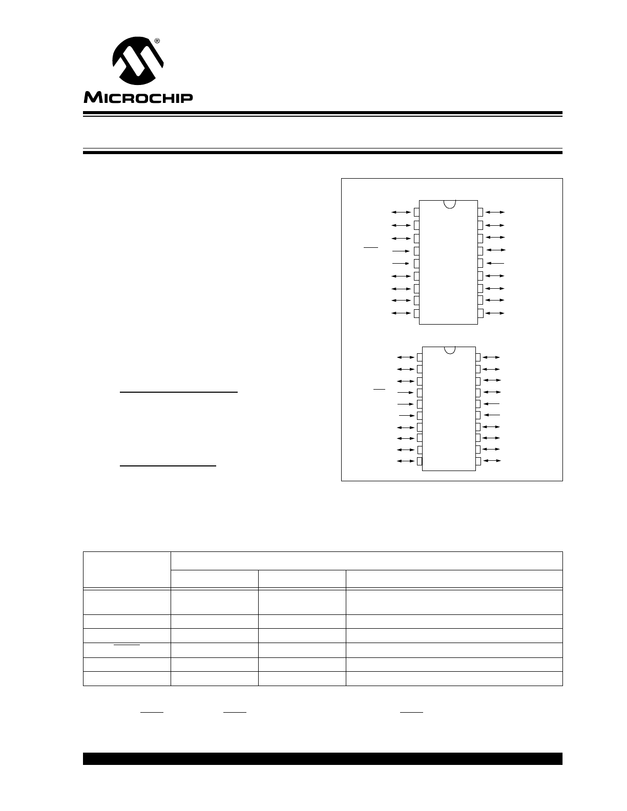
Pin Diagram
PDIP, SOIC
RA2/AN2/V
REF
RA3/AN3/CMP1
RA4/T0CKI/CMP2
RA5/MCLR/THV
V
SS
RB0/INT
RB1/RX/DT
RB2/TX/CK
RB3/CCP1
RA1/AN1
RA0/AN0
RA7/OSC1/CLKIN
RA6/OSC2/CLKOUT
V
DD
RB7/T1OSI
RB6/T1OSO/T1CKI
RB5
RB4/PGM
• 1
2
3
4
5
7
8
9
18
17
16
15
14
12
11
10
PIC1
6F62X
6
13
RA2/AN2/V
REF
RA3/AN3/CMP1
RA4/T0CKI/CMP2
RA5/MCLR/THV
V
SS
RB0/INT
RB1/RX/DT
RB2/TX/CK
RB3/CCP1
RA1/AN1
RA0/AN0
RA7/OSC1/CLKIN
RA6/OSC2/CLKOUT
V
DD
RB7/T1OSI
RB6/T1OSO/T1CKI
RB5
RB4/PGM
• 1
2
3
4
5
7
8
9
18
17
16
15
14
12
11
10
P
IC1
6F62
X
6
13
V
DD
V
SS
19
20
PIN DESCRIPTIONS (DURING PROGRAMMING): PIC16F62X
Pin Name
During Programming
Function
Pin Type
Pin Description
RB4
PGM
I
Low voltage programming input if configuration bit
equals 1
RB6
CLOCK
I
Clock input
RB7
DATA
I/O
Data input/output
MCLR
V
TEST MODE
P*
Program Mode Select
V
DD
V
DD
P
Power Supply
V
SS
V
SS
P
Ground
Legend: I = Input, O = Output, P = Power
* In the PIC16F62X, the programming high voltage is internally generated. To activate the programming mode, high voltage needs to
be applied to MCLR input. Since the MCLR is used for a level source, this means that MCLR does not draw any significant current.
EEPROM Memory Programming Specification
PIC16F62X
DS30034B-page 2
Preliminary
2000 Microchip Technology Inc.
2.0
PROGRAM MODE ENTRY
2.1
User Program Memory Map
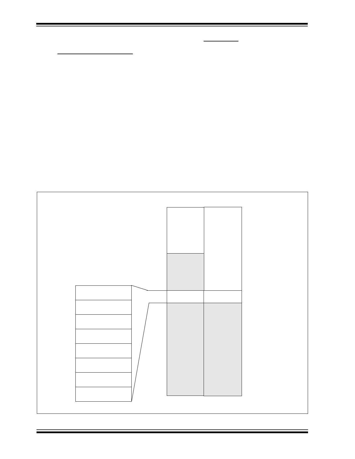
The user memory space extends from 0x0000 to
0x7FFF. In programming mode, the program memory
space extends from 0x0000 to 0x3FFF, with the first
half (0x0000-0x7FFF) being user program memory and
the second half (0x2000-0x3FFF) being configuration
memory. The PC will increment from 0x0000 to 0x7FFF
and wrap to 0x000, 0x2000 to 0x3FFF and wrap
around to 0x2000 (not to 0x0000). Once in configura-
tion memory, the highest bit of the PC stays a ‘1’, thus
always pointing to the configuration memory. The only
way to point to user program memory is to reset the
part and reenter program/verify mode as described in
Section 2.3.
In the configuration memory space, 0x2000-0x200F
are physically implemented. However, only locations
0x2000 through 0x2007 are available. Other locations
are reserved. Locations beyond 0x200F will physically
access user memory (See Figure 2-1).
2.2
ID Locations
A user may store identification information (ID) in four
ID locations. The ID locations are mapped in [0x2000 :
0x2003]. It is recommended that the user use only the
four least significant bits of each ID location. In some
devices, the ID locations read-out in an unscrambled
fashion after code protection is enabled. For these
devices, it is recommended that ID location is written as
“
11 1111 1000 bbbb
” where ‘
bbbb
’ is ID information.
In other devices, the ID locations read out normally,
even after code protection. To understand how the
devices behave, refer to Table 4-1.
To understand the scrambling mechanism after code
protection, refer to Section 3-1.
FIGURE 2-1:
PROGRAM MEMORY MAPPING
1FFF
2000
ID Location
ID Location
ID Location
ID Location
Reserved
Reserved
Reserved
Configuration Word
2000
2001
2002
2003
2005
2006
2007
2008
3FFF
0x1FF
Not Implemented
Implemented
1 KW
Implemented
2004
Implemented
2 KW
Implemented
2000 Microchip Technology Inc.
Preliminary
DS30034B-page 3
PIC16F62X
2.3
Program/Verify Mode
The program/verify mode is entered by holding pins
RB6 and RB7 low while raising MCLR pin from V
IL
to
V
IHH
(high voltage), or by applying V
DD
to MCLR and
raising RB3 from V
IL
to V
DD
. Once in this mode, the
user program memory and the configuration memory
can be accessed and programmed in serial fashion.
The mode of operation is serial, and the memory that is
accessed is the user program memory. RB6 and RB7
are Schmitt Trigger Inputs in this mode.
The sequence that enters the device into the program-
ming/verify mode places all other logic into the RESET
state (the MCLR pin was initially at V
IL
). This means
that all I/O are in the RESET state (high impedance
inputs).
The normal sequence for programming is to use the
load data command to set a value to be written at the
selected address. Issue the begin programming com-
mand followed by read data command to verify, and
then increment the address.
A device RESET will clear the PC and set the address
to 0. The “increment address” command will increment
the PC. The “load configuration” command will set the
PC to 0x2000. The available commands are shown in
Table 2-1.
2.3.1
LOW VOLTAGE PROGRAMMING MODE
When LVP bit is set to ‘1’, the low voltage programming
entry is enabled. Since the LVP configuration bit allows
low voltage programming entry in its erased state, an
erased device will have the LVP bit enabled at the fac-
tory. While LVP is ‘1’, RB4 is dedicated to low voltage
programming. Bring MCLR to V
DD
and then RB4 to
V
DD
to enter programming mode. All other specifica-
tions for high voltage ICSP™ apply.
To disable low voltage mode, the LVP bit must be pro-
grammed to ‘0’. This must be done while entered with
high voltage entry mode (LVP bit = 1). RB4 is now a
general purpose I/O pin.
2.3.2
SERIAL PROGRAM/VERIFY OPERATION
The RB6 pin is used as a clock input pin, and the RB7
pin is used for entering command bits and data input/
output during serial operation. To input a command, the
clock pin (RB6) is cycled six times. Each command bit
is latched on the falling edge of the clock with the least
significant bit (LSb) of the command being input first.
The data on pin RB7 is required to have a minimum
setup and hold time (see AC/DC specifications), with
respect to the falling edge of the clock. Commands that
have data associated with them (read and load) are
specified to have a minimum delay of 1
µ
s between the
command and the data. After this delay, the clock pin is
cycled 16 times with the first cycle being a Start bit and
the last cycle being a Stop bit. Data is also input and
output LSb first.
Therefore, during a read operation the LSb will be
transmitted onto pin RB7 on the rising edge of the sec-
ond cycle, and during a load operation the LSb will be
latched on the falling edge of the second cycle. A min-
imum 1
µ
s delay is also specified between consecutive
commands.
All commands are transmitted LSb first. Data words
are also transmitted LSb first. The data is transmitted
on the rising edge and latched on the falling edge of
the clock. To allow for decoding of commands and
reversal of data pin configuration, a time separation of
at least 1
µ
s is required between a command and a
data word (or another command).
The commands that are available are:
2.3.2.1
LOAD CONFIGURATION
After receiving this command, the program counter
(PC) will be set to 0x2000. By then applying 16 cycles
to the clock pin, the chip will load 14-bits in a “data
word,” as described above, to be programmed into the
configuration memory. A description of the memory
mapping schemes of the program memory for normal
operation and configuration mode operation is shown
in Figure 2-1. After the configuration memory is
entered, the only way to get back to the user program
memory is to exit the program/verify test mode by tak-
ing MCLR low (V
IL
).
Note:
The OSC must not have 72 osc clocks
while the device MCLR is between V
IL
and
V
IHH
.

PIC16F62X
DS30034B-page 4
Preliminary
2000 Microchip Technology Inc.
2.3.2.2
LOAD DATA FOR PROGRAM MEMORY
After receiving this command, the chip will load in a
14-bit “data word” when 16 cycles are applied, as
described previously. A timing diagram for the load
data command is shown in Figure 5-1.
TABLE 2-1:
COMMAND MAPPING FOR PIC16F627/PIC16F628
Command
Mapping (MSb … LSb)
Data
Load Configuration
X
X
0
0
0
0
0, data (14), 0
Load Data for Program Memory
X
X
0
0
1
0
0, data (14), 0
Read Data from Program Memory
X
X
0
1
0
0
0, data (14), 0
Increment Address
X
X
0
1
1
0
Begin Erase Programming Cycle
0
0
1
0
0
0
Begin Programming Only Cycle
0
1
1
0
0
0
Load Data for Data Memory
X
X
0
0
1
1
0, data (14), 0
Read Data from Data Memory
X
X
0
1
0
1
0, data (14), 0
Bulk Erase Program Memory
X
X
1
0
0
1
Bulk Erase Data Memory
X
X
1
0
1
1
2000 Microchip Technology Inc.
Preliminary
DS30034B-page 5
PIC16F62X
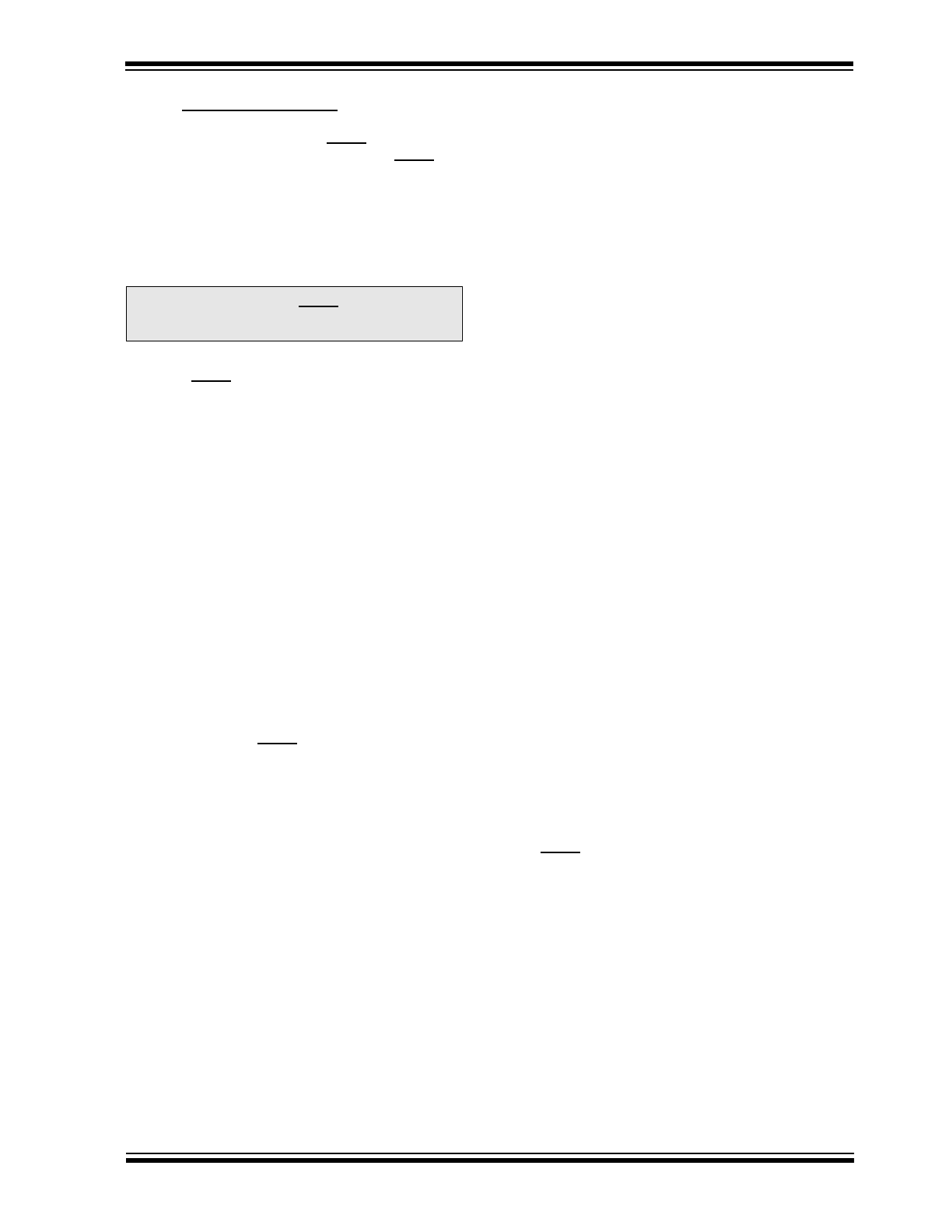
FIGURE 2-2:
PROGRAM FLOW CHART - PIC16F62X PROGRAM MEMORY
Start
Set V
DD
= V
DDP
Program Cycle
Read Data
Command
Data Correct?
Report
Programming
Failure
All Locations
Done?
Verify all
Locations @
V
DDMIN
Data Correct?
Verify all
Locations @
V
DDMAX
Data Correct?
Done
Increment
Address
Command
Report Verify
Error @
V
DDMIN
Report Verify
Error @
V
DDMAX
Load Data
Command
Begin
Programming
Command
Wait 2 ms
PROGRAM CYCLE
No
No
No
No
PIC16F62X
DS30034B-page 6
Preliminary
2000 Microchip Technology Inc.
FIGURE 2-3:
PROGRAM FLOW CHART - PIC16F62X CONFIGURATION MEMORY
Program ID
Start
Load
Configuration
Data
Location?
Program Cycle
Read Data
Command
Data Correct?
Report
Programming
Failure
Increment
Address
Command
Address =
0x2004?
Increment
Address
Command
Increment
Address
Command
Increment
Address
Command
Program
Cycle
(Config. Word)
Set V
DD
=
V
DDMAX
Read Data
Command
Data Correct?
Set V
DD
=
V
DDMAX
Read Data
Command
Data Correct?
Report Program
Configuration
Word Error
Done
Yes
No
No
Yes
Yes
No
No
Yes
Yes
No

2000 Microchip Technology Inc.
Preliminary
DS30034B-page 7
PIC16F62X
2.3.2.3
LOAD DATA FOR DATA MEMORY
After receiving this command, the chip will load in a
14-bit “data word” when 16 cycles are applied. How-
ever, the data memory is only 8-bits wide, and thus only
the first 8-bits of data after the Start bit will be pro-
grammed into the data memory. It is still necessary to
cycle the clock the full 16 cycles in order to allow the
internal circuitry to reset properly. The data memory
contains 64 words. Only the lower 8-bits of the PC are
decoded by the data memory, and therefore, if the PC
is greater than 0x3F, it will wrap around and address a
location within the physically implemented memory. If
the device is code protected, the data is read as all
zeros.
2.3.2.4
READ DATA FROM PROGRAM
MEMORY
After receiving this command, the chip will transmit
data bits out of the program memory (user or configu-
ration) currently accessed, starting with the second ris-
ing edge of the clock input. The RB7 pin will go into
output mode on the second rising clock edge, and it will
revert back to input mode (hi-impedance) after the 16th
rising edge. A timing diagram of this command is
shown in Figure 5-2.
2.3.2.5
READ DATA FROM DATA MEMORY
After receiving this command, the chip will transmit
data bits out of the data memory starting with the sec-
ond rising edge of the clock input. The RB7 pin will go
into output mode on the second rising edge, and it will
revert back to input mode (hi-impedance) after the 16th
rising edge. As previously stated, the data memory is
8-bits wide, and therefore, only the first 8-bits that are
output are actual data.
2.3.2.6
INCREMENT ADDRESS
The PC is incremented when this command is
received. A timing diagram of this command is shown
in Figure 5-3.
2.3.2.7
BEGIN ERASE/PROGRAM CYCLE
A load command must be given before every begin
programming command. Programming of the appro-
priate memory (test program memory, user program
memory or data memory) will begin after this command
is received and decoded. An internal timing mechanism
executes an erase before write. The user must allow for
both erase and programming cycle times for program-
ming to complete. No “end programming” command is
required.
2.3.2.8
BEGIN PROGRAMMING
A load command must be given before every begin
programming command. Programming of the appro-
priate memory (test program memory, user program
memory or data memory) will begin after this command
is received and decoded. An internal timing mechanism
executes a write. The user must allow for program
cycle time for programming to complete. No “end pro-
gramming” command is required.
This command is similar to the ERASE/PROGRAM
CYCLE command, except that a word erase is not
done. It is recommended that a bulk erase be per-
formed before starting a series of programming only
cycles.
2.3.2.9
BULK ERASE PROGRAM MEMORY
After this command is performed, the next program
command will erase the entire program memory.
To perform a bulk erase of the program memory, the fol-
lowing sequence must be performed.
1.
Do a “Load Data All 1’s” command.
2.
Do a “Bulk Erase User Memory” command.
3.
Do a “Begin Programming” command.
4.
Wait 10 ms to complete bulk erase.
If the address is pointing to the test program memory
(0x2000 - 0x200F), then both the user memory and the
test memory will be erased. The configuration word will
not be erased, even if the address is pointing to loca-
tion 0x2007.
2.3.2.10
BULK ERASE DATA MEMORY
To perform a bulk erase of the data memory, the follow-
ing sequence must be performed.
1.
Do a “Load Data All 1’s” command.
2.
Do a “Bulk Erase Data Memory” command.
3.
Do a “Begin Programming” command.
4.
Wait 10 ms to complete bulk erase.
Note:
If the device is code-protected, the BULK
ERASE command will not work.
Note:
All BULK ERASE operations must take
place at 4.5 to 5.5 V
DD
range.

PIC16F62X
DS30034B-page 8
Preliminary
2000 Microchip Technology Inc.
2.4
Programming Algorithm Requires
Variable V
DD
The PIC16F62X uses an intelligent algorithm. The
algorithm calls for program verification at V
DDMIN
as
well as V
DDMAX
. Verification at V
DDMIN
guarantees
good “erase margin”. Verification at V
DDMAX
guaran-
tees good “program margin”.
The actual programming must be done with V
DD
in the
V
DDP
range (See Table 5-1).
V
DDP
= V
CC
range required during programming.
V
DDMIN
= minimum
operating
V
DD
spec for the part.
V
DDMAX
= maximum operating V
DD
spec for the part.
Programmers must verify the PIC16F62X at its speci-
fied V
DDMAX
and V
DDMIN
levels. Since Microchip may
introduce future versions of the PIC16F62X with a
broader V
DD
range, it is best that these levels are user
selectable (defaults are ok).
Note:
Any programmer not meeting these
requirements may only be classified as
“prototype” or “development” programmer,
but not a “production” quality programmer.
2000 Microchip Technology Inc.
Preliminary
DS30034B-page 9
PIC16F62X
3.0
CONFIGURATION WORD
The PIC16F62X has several configuration bits. These
bits can be set (reads ‘0’), or left unchanged (reads ‘1’),
to select various device configurations.
3.1
Device ID Word
The device ID word for the PIC16F62X is located at
2006h.
FIGURE 3-1:
CONFIGURATION WORD FOR PIC16F627/628
TABLE 3-1:
Device
Device ID Value
Dev
Rev
PIC16F627
00 0111 111
x xxxx
PIC16F628
00 0111 001
x xxxx
CP1
CP0 CP1
CP0
-
CPD LVP
BODEN
MCLRE
FOSC2
PWRTE
WDTE
F0SC1
F0SC0
Register:
CONFIG
Address
2007h
bit13
bit0
bit 13-10: CP1:CP0: Code Protection bits
(2)
Code protection for 2K program memory
11
= Program memory code protection off
10
= 0400h-07FFh code protected
01
= 0200h-07FFh code protected
00
= 0000h-07FFhcode protected
Code protection for 1K program memory
11
= Program memory code protection off
10
= Program memory code protection off
01
= 0200h-03FFh code protected
00
= 0000h-03FFh code protected
bit 8:
CPD: Data Code Protection bit
(3)
1
= Data memory code protection off
0
= Data memory code protected
bit 7:
LVP: Low Voltage Programming Enable
1 = RB4/PGM pin has PGM function, low voltage programming enabled
0 = RB4/PGM is digital I/O, HV on MCLR must be used for programming
bit 6:
BODEN: Brown-out Detect Reset Enable bit
(1)
1 = BOD Reset enabled
0 = BOD Reset disabled
bit 5:
MCLRE: RA5/MCLR Pin Function Select
1 = RA5/MCLR pin function is MCLR
0 = RA5/MCLR pin function is digital I/O, MCLR internally tied to V
DD
bit 3:
PWRTE: Power-up Timer Enable bit
(1)
1 = PWRT disabled
0 = PWRT enabled
bit 2:
WDTE: Watchdog Timer Enable bit
1 = WDT enabled
0 = WDT disabled
bit 4,1-0: FOSC2:FOSC0: Oscillator Selection bits
(4)
111
= ER oscillator: CLKOUT function on RA6/OSC2/CLKOUT pin, Resistor on RA7/OSC1/CLKIN
110
= ER oscillator: I/O function on RA6/OSC2/CLKOUT pin, Resistor on RA7/OSC1/CLKIN
101
= INTRC oscillator: CLKOUT function on RA6/OSC2/CLKOUT pin, I/O function on RA7/OSC1/CLKIN
100
= INTRC oscillator: I/O function on RA6/OSC2/CLKOUT pin, I/O function on RA7/OSC1/CLKIN
011
= E
XT
C
LK
: I/O function on RA6/OSC2/CLKOUT pin, CLKIN on RA7/OSC1/CLKIN
010
= HS oscillator: High speed crystal/resonator on RA6/OSC2/CLKOUT and RA7/OSC1/CLKIN
001
= XT oscillator: Crystal/resonator on RA6/OSC2/CLKOUT and RA7/OSC1/CLKIN
000
= LP oscillator: Low power crystal on RA6/OSC2/CLKOUT and RA7/OSC1/CLKIN
Note 1: Enabling Brown-out Reset automatically enables Power-up Timer (PWRT) regardless of the value of bit PWRTE. Ensure
the Power-up Timer is enabled any time Brown-out Reset is enabled.
2: All of the CP1:CP0 pairs have to be given the same value to enable the code protection scheme listed. The entire pro-
gram EEPROM will be erased if the code protection is reduced.
3: The entire data EEPROM will be erased when the code protection is turned off. The calibration space in the test memory
is not erased.
4: When MCLR is asserted in INTRC or ER mode, the internal clock oscillator is disabled.

PIC16F62X
DS30034B-page 10
Preliminary
2000 Microchip Technology Inc.
4.0
CODE PROTECTION
For PIC16F62X devices, once code protection is
enabled, all program memory locations read all 0’s.
The ID locations and the configuration word read out in
an unscrambled fashion. Further programming is dis-
abled for the entire program memory, as well as data
memory. It is possible to program the ID locations and
the configuration word.
4.1
Disabling Code Protection
It is recommended that the following procedure be per-
formed before any other programming is attempted. It
is also possible to turn code protection off (code protect
bit = 1) using this procedure; however, all data within
the program memory and the data memory will be
erased when this procedure is executed, and thus,
the security of the data or code is not compro-
mised.
Procedure to disable code protect:
a)
Execute load configuration (
111111
).
b)
Increment to configuration word location
(0x2007).
c)
Execute command (
000001
).
d)
Execute command (
000111
).
e)
Execute ‘Begin Programming’ (
001000
).
f)
Wait 10 ms.
g)
Execute command (
000001
).
h)
Execute command (
000111
).
4.2
Embedding Configuration Word and ID Information in the Hex File
To allow portability of code, the programmer is required to read the configuration word and ID locations from the hex
file when loading the hex file. If configuration word information was not present in the hex file, then a simple warning
message may be issued. Similarly, while saving a hex file, configuration word and ID information must be included.
An option to not include this information may be provided.
Specifically for the PIC16F62X, the EEPROM data memory should also be embedded in the hex file (see
Section 5.1).
Microchip Technology Inc. feels strongly that this feature is important for the benefit of the end customer.

2000 Microchip Technology Inc.
Preliminary
DS30034B-page 11
PIC16F62X
4.3
Checksum Computation
4.3.1
CHECKSUM
Checksum is calculated by reading the contents of the
PIC16F62X memory locations and adding up the
opcodes up to the maximum user addressable location,
e.g., 0x1FF for the PIC16F62X. Any carry bits exceed-
ing 16-bits are neglected. Finally, the configuration
word (appropriately masked) is added to the check-
sum. Checksum computation for each member of the
PIC16F62X devices is shown in Table 4-1.
The checksum is calculated by summing the following:
• The contents of all program memory locations
• The configuration word, appropriately masked
• Masked ID locations (when applicable)
The least significant 16 bits of this sum is the check-
sum.
The following table describes how to calculate the
checksum for each device. Note that the checksum cal-
culation differs depending on the code protect setting.
Since the program memory locations read out differ-
ently depending on the code protect setting, the table
describes how to manipulate the actual program mem-
ory values to simulate the values that would be read
from a protected device. When calculating a checksum
by reading a device, the entire program memory can
simply be read and summed. The configuration word
and ID locations can always be read.
Note that some older devices have an additional value
added in the checksum. This is to maintain compatibil-
ity with older device programmer checksums.
TABLE 4-1:
CHECKSUM COMPUTATION
Device
Code
Protect
Checksum*
Blank
Value
0x25E6 at 0
and max
address
PIC16F627
OFF
SUM[0x0000:0x3FFF] + CFGW & 0x3DFF
0x39FF
0x05CD
0x200 : 0x3FF
SUM[0x0000:0x01FF] + CFGW & 0x3DFF + SUM_ID
0x4DFE
0xFFB3
ALL
CFGW & 0x3DFF + SUM_ID
0x3BFE
0x07CC
PIC16F628
OFF
SUM[0x0000:0x07FF] + CFGW & 0x3DFF
0x35FF
0x01CD
0x400 : 0xFFF
SUM[0x0000:0x03FF] + CFGW & 0x3DFF +SUM_ID
0x5BFE
0x0DB3
0x200 : 0x7FF
SUM[0x0000:0x01FF] + CFGW & 0x3DFF + SUM_ID
0x49FE
0xFBB3
ALL
CFGW & 0x3DFF + SUM_ID
0x37FE
0x03CC
Legend: CFGW = Configuration Word
SUM[a:b] = [Sum of locations a to b inclusive]
SUM_ID = ID locations masked by 0xF then made into a 16-bit value with ID0 as the most significant nibble.
For example, ID0 = 0x1, ID1 = 0x2, ID3 = 0x3, ID4 = 0x4, then SUM_ID = 0x1234
*Checksum = [Sum of all the individual expressions] MODULO [0xFFFF]
+ = Addition
& = Bitwise AND
PIC16F62X
DS30034B-page 12
Preliminary
2000 Microchip Technology Inc.
5.0
PROGRAM/VERIFY MODE ELECTRICAL CHARACTERISTICS
5.1
Embedding Data EEPROM Contents in Hex File
The programmer should be able to read data EEPROM information from a hex file and conversely (as an option), write
data EEPROM contents to a hex file along with program memory information and fuse information.
The 64 data memory locations are logically mapped starting at address 0x2100. The format for data memory storage is
one data byte per address location, LSB aligned.
TABLE 5-1:
AC/DC CHARACTERISTICS
TIMING REQUIREMENTS FOR PROGRAM/VERIFY MODE
Standard Operating Conditions (unless otherwise stated)
Operating Temperature:
0°C
≤
T
A
≤
+70°C
Operating Voltage:
4.5V
≤
V
DD
≤
5.5V
Characteristics
Sym
Min
Typ
Max
Units
Conditions/Comments
General
V
DD
level for word operations, program
memory
V
DD
2.0
5.5
V
V
DD
level for word operations, data
memory
V
DD
2.0
5.5
V
V
DD
level for bulk erase/write operations,
program and data memory
V
DD
4.5
5.5
V
High voltage on MCLR and
RA4/T0CKI for test mode entry
V
IHH
V
DD
+ 3.5
13.5
V
MCLR rise time (V
SS
to V
HH
) for test
mode entry
t
VHHR
1.0
µ
s
Hold time after V
PP
↑
T
PPDP
5
µ
s
(RB6, RB7) input high level
V
IH
1
0.8V
DD
V
Schmitt Trigger input
(RB6, RB7) input low level
V
IL
1
0.2V
DD
V
Schmitt Trigger input
RB<7:4> setup time before MCLR
↑
(test mode selection pattern setup time)
tset0
100
ns
RB<7:4> hold time after MCLR
↑
(test mode selection pattern setup time)
thld0
5
µ
s
Serial Program/Verify
Data in setup time before clock
↓
tset
1
100
ns
Data in hold time after clock
↓
thld
1
100
ns
Data input not driven to next clock input
(delay required between command/data or
command/command)
tdly
1
1.0
µ
s
Delay between clock
↓
to clock
↑
of next
command or data
tdly2
1.0
µ
s
Clock
↑
to data out valid (during read data)
tdly3
80
ns
Erase cycle time
tera
2
5
ms
Programming cycle time
tprog
2
5
ms
Time delay from program to compare (HV
discharge time)
tdis
0.5
µ
s
2000 Microchip Technology Inc.
Preliminary
DS30034B-page 13
PIC16F62X
FIGURE 5-1:
LOAD DATA COMMAND (PROGRAM/VERIFY)
FIGURE 5-2:
READ DATA COMMAND (PROGRAM/VERIFY)
FIGURE 5-3:
INCREMENT ADDRESS COMMAND (PROGRAM/VERIFY)
MCLR
V
IHH
tset0
RB6
(CLOCK)
RB7
(DATA)
RESET
tset1
thld1
tdly1
1
µ
s min.
Program/Verify Test Mode
tset1
thld1
100ns min.
1
µ
s min.
tdly2
1
2
3
4
5
6
0
1
0
0
X
X
1
2
3
4
5
15
16
strt_bit
stp_bit
100ns min.
}
thld0
}
} }
V
DD
T
PPDP
MCLR
V
IHH
tset0
RB6
(CLOCK)
RB7
(DATA)
RESET
tdly1
1
µ
s min.
Program/Verify Test Mode
tset1
thld1
1
µ
s min.
tdly2
1
2
3
4
5
6
1
0
1
0
X
X
1
2
3
4
5
15
16
100ns min.
} }
tdly3
RB7 = input
RB7 = output
RB7
input
thld0
strt_bit
stp_bit
T
PPDP
V
DD
MCLR
V
IHH
RB6
(CLOCK)
RB7
(DATA)
RESET
tdly1
1
µ
s min.
Program/Verify Test Mode
tset1
thld1
1
µ
s min.
tdly2
1
2
3
4
5
6
0
1
1
X
X
1
2
100ns min.
} }
X
0
0
Next Command
T
PPDP
V
DD
Information contained in this publication regarding device applications and the like is intended through suggestion only and may be superseded by updates.
It is your responsibility to ensure that your application meets with your specifications. No representation or warranty is given and no liability is assumed by
Microchip Technology Incorporated with respect to the accuracy or use of such information, or infringement of patents or other intellectual property rights
arising from such use or otherwise. Use of Microchip’s products as critical components in life support systems is not authorized except with express written
approval by Microchip. No licenses are conveyed, implicitly or otherwise, except as maybe explicitly expressed herein, under any intellectual property
rights. The Microchip logo and name are registered trademarks of Microchip Technology Inc. in the U.S.A. and other countries. All rights reserved. All other
trademarks mentioned herein are the property of their respective companies.
DS30034B-page 14
Preliminary
2000 Microchip Technology Inc.
All rights reserved. © 2000 Microchip Technology Incorporated. Printed in the USA. 8/00
Printed on recycled paper.
AMERICAS
Corporate Office
Microchip Technology Inc.
2355 West Chandler Blvd.
Chandler, AZ 85224-6199
Tel: 480-786-7200 Fax: 480-786-7277
Technical Support: 480-786-7627
Web Address: http://www.microchip.com
Atlanta
Microchip Technology Inc.
500 Sugar Mill Road, Suite 200B
Atlanta, GA 30350
Tel: 770-640-0034 Fax: 770-640-0307
Boston
Microchip Technology Inc.
2 LAN Drive, Suite 120
Westford, MA 01886
Tel: 508-480-9990 Fax: 508-480-8575
Chicago
Microchip Technology Inc.
333 Pierce Road, Suite 180
Itasca, IL 60143
Tel: 630-285-0071 Fax: 630-285-0075
Dallas
Microchip Technology Inc.
4570 Westgrove Drive, Suite 160
Addison, TX 75001
Tel: 972-818-7423 Fax: 972-818-2924
Dayton
Microchip Technology Inc.
Two Prestige Place, Suite 150
Miamisburg, OH 45342
Tel: 937-291-1654 Fax: 937-291-9175
Detroit
Microchip Technology Inc.
Tri-Atria Office Building
32255 Northwestern Highway, Suite 190
Farmington Hills, MI 48334
Tel: 248-538-2250 Fax: 248-538-2260
Los Angeles
Microchip Technology Inc.
18201 Von Karman, Suite 1090
Irvine, CA 92612
Tel: 949-263-1888 Fax: 949-263-1338
New York
Microchip Technology Inc.
150 Motor Parkway, Suite 202
Hauppauge, NY 11788
Tel: 631-273-5305 Fax: 631-273-5335
San Jose
Microchip Technology Inc.
2107 North First Street, Suite 590
San Jose, CA 95131
Tel: 408-436-7950 Fax: 408-436-7955
AMERICAS
(continued)
Toronto
Microchip Technology Inc.
5925 Airport Road, Suite 200
Mississauga, Ontario L4V 1W1, Canada
Tel: 905-405-6279 Fax: 905-405-6253
ASIA/PACIFIC
China - Beijing
Microchip Technology, Beijing
Unit 915, 6 Chaoyangmen Bei Dajie
Dong Erhuan Road, Dongcheng District
New China Hong Kong Manhattan Building
Beijing, 100027, P.R.C.
Tel: 86-10-85282100 Fax: 86-10-85282104
China - Shanghai
Microchip Technology
Unit B701, Far East International Plaza,
No. 317, Xianxia Road
Shanghai, 200051, P.R.C.
Tel: 86-21-6275-5700 Fax: 86-21-6275-5060
Hong Kong
Microchip Asia Pacific
Unit 2101, Tower 2
Metroplaza
223 Hing Fong Road
Kwai Fong, N.T., Hong Kong
Tel: 852-2-401-1200 Fax: 852-2-401-3431
India
Microchip Technology Inc.
India Liaison Office
Divyasree Chambers
I Floor, Wing A (A3/A4)
No. 11, O’Shaugnessey Road
Bangalore, 560 027, India
Tel: 91-80-207-2165 Fax: 91-80-207-2171
Japan
Microchip Technology Intl. Inc.
Benex S-1 6F
3-18-20, Shinyokohama
Kohoku-Ku, Yokohama-shi
Kanagawa, 222-0033, Japan
Tel: 81-45-471- 6166 Fax: 81-45-471-6122
Korea
Microchip Technology Korea
168-1, Youngbo Bldg. 3 Floor
Samsung-Dong, Kangnam-Ku
Seoul, Korea
Tel: 82-2-554-7200 Fax: 82-2-558-5934
ASIA/PACIFIC
(continued)
Singapore
Microchip Technology Singapore Pte Ltd.
200 Middle Road
#07-02 Prime Centre
Singapore, 188980
Tel: 65-334-8870 Fax: 65-334-8850
Taiwan
Microchip Technology Taiwan
11F-3, No. 207
Tung Hua North Road
Taipei, 105, Taiwan
Tel: 886-2-2717-7175 Fax: 886-2-2545-0139
EUROPE
Denmark
Microchip Technology Denmark ApS
Regus Business Centre
Lautrup hoj 1-3
Ballerup DK-2750 Denmark
Tel: 45 4420 9895 Fax: 45 4420 9910
France
Arizona Microchip Technology SARL
Parc d’Activite du Moulin de Massy
43 Rue du Saule Trapu
Batiment A - ler Etage
91300 Massy, France
Tel: 33-1-69-53-63-20 Fax: 33-1-69-30-90-79
Germany
Arizona Microchip Technology GmbH
Gustav-Heinemann-Ring 125
D-81739 München, Germany
Tel: 49-89-627-144 0 Fax: 49-89-627-144-44
Italy
Arizona Microchip Technology SRL
Centro Direzionale Colleoni
Palazzo Taurus 1 V. Le Colleoni 1
20041 Agrate Brianza
Milan, Italy
Tel: 39-039-65791-1 Fax: 39-039-6899883
United Kingdom
Arizona Microchip Technology Ltd.
505 Eskdale Road
Winnersh Triangle
Wokingham
Berkshire, England RG41 5TU
Tel: 44 118 921 5858 Fax: 44-118 921-5835
8/01/00
W
ORLDWIDE
S
ALES
AND
S
ERVICE
Microchip received QS-9000 quality system
certification for its worldwide headquarters,
design and wafer fabrication facilities in
Chandler and Tempe, Arizona in July 1999. The
Company’s quality system processes and
procedures are QS-9000 compliant for its
PICmicro
®
8-bit MCUs, K
EE
L
OQ
®
code hopping
devices, Serial EEPROMs and microperipheral
products. In addition, Microchip’s quality
system for the design and manufacture of
development systems is ISO 9001 certified.