
2002-2012 Microchip Technology Inc.
DS21417C-page 1
TC4403
Features
• Low Quiescent Current: 300
A Max
• Capacitive Inputs With 300mV Hysteresis
• Both Inputs Must Be Driven to Drive Load
• Low Output Leakage
• High Peak Current Capability
• Fast Output Rise Time
• Outputs Individually Testable
Applications
• Isolated Load Drivers
• Pulsers
• Safety Interlocks
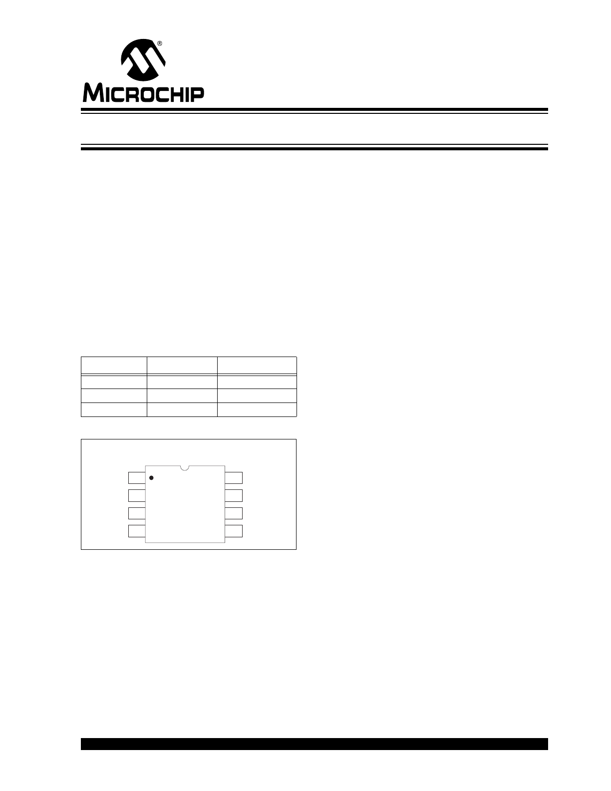
Device Selection Table
Package Type
General Description
The TC4403 is a modified version of the TC4425 driver,
intended to drive floating or isolated loads requiring
high-current pulses. The load is intended to be con-
nected between the outputs without other reference to
supply or ground. Then, only when both logic inputs
and the V
DD
input are energized, is power supplied to
the load. This construction allows the implementation
of a wide variety of redundant input controllers.
The low OFF-state output leakage and independence
of the two half-circuits permit a wide variety of testing
schemes to be utilized to assure functionality. The high
peak current capability, short internal delays, and fast
output rise and fall times ensure that sufficient power
will be available to the load when it is needed. The TTL
and CMOS compatible inputs allow operation from a
wide variety of input devices. The ability to swing the
inputs negative without affecting device performance
allows negative biases to be placed on the inputs for
greater safety. In addition, the capacitive nature of the
inputs allows the use of series resistors on the inputs
for extra noise suppression.
The TC4403 is built for outstanding ruggedness and
reliability in harsh applications. Input voltage excur-
sions above the supply voltage or below ground are
clamped internally without damaging the device. The
output stages are power MOSFETs with high-speed
body diodes to prevent damage to the driver from
inductive kickbacks.
Part Number
Package
Temp. Range
TC4403CPA
8-Pin PDIP
0°C to +70°C
TC4403EPA
8-Pin PDIP
-40°C to +85°C
TC4403MJA
8-Pin CERDIP
-55°C to +125°C
1
8
2
7
3
6
4
5
TC4403
OUT (GND)
IN (GND)
GND
IN (V
DD
)
V
DD
OUT (V
DD
)
NC
NC
8-Pin PDIP/CERDIP
1.5A High-Speed, Floating Load Driver
TC4403
DS21417C-page 2
2002-2012 Microchip Technology Inc.
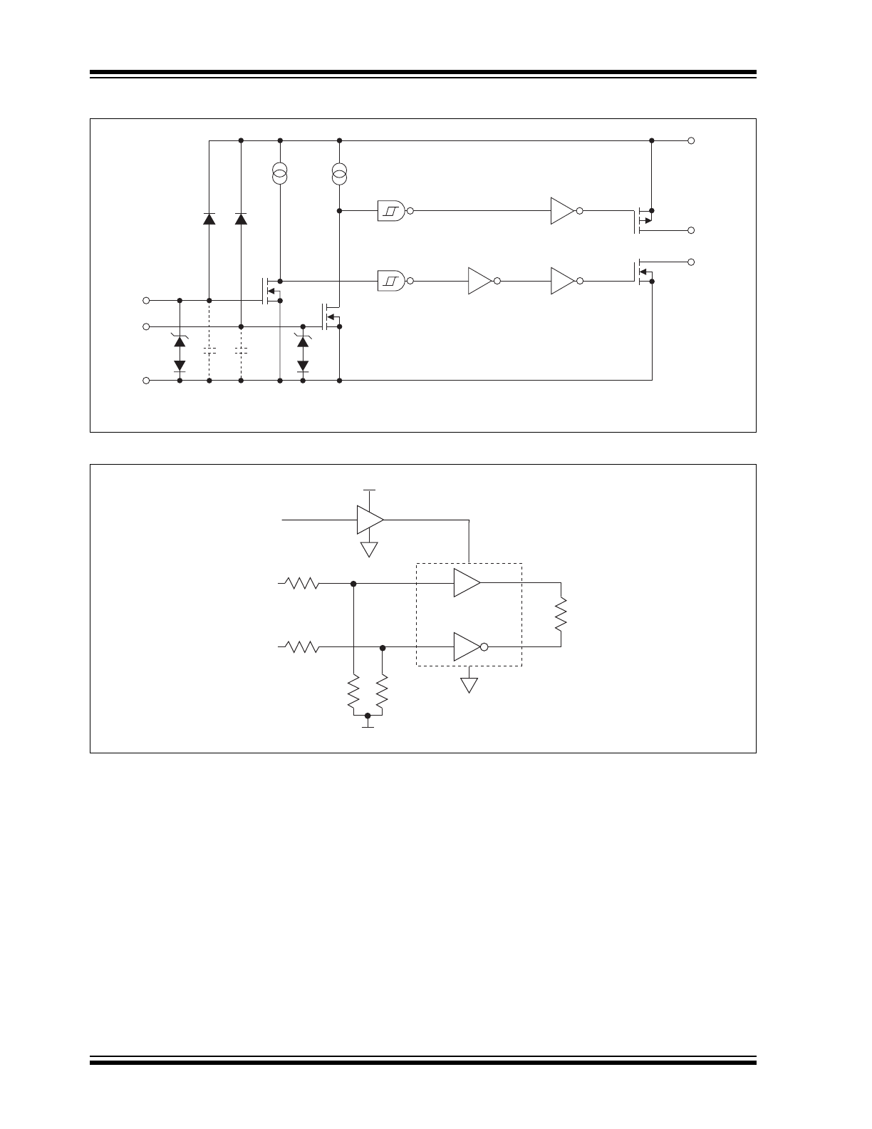
Functional Block Diagram
Typical Application
TC4403
300mV Input
Hysteresis
Effective Input
C = 20pF
(Each Input)
GND
IN (V
DD
)
IN (GND)
4
2
3
OUT (V
DD
)
OUT (GND)
V
DD
6
7
5
2
4
3
5
7
6
Power
1 M
Ω
R
LOAD
TC4403
3
6
-15V
1 M
Ω
+15V
R
T
R
T
TC4422
Fire
Arm
2002-2012 Microchip Technology Inc.
DS21417C-page 3
TC4403
1.0
ELECTRICAL
CHARACTERISTICS
Absolute Maximum Ratings*
Supply Voltage..................................................... +22V
Package Thermal Resistance
CERDIP R
J-A
........................................ 150
C/W
CERDIP R
J-C
......................................... 50°C/W
PDIP R
J-A
............................................. 125°C/W
PDIP R
J-C
............................................... 42°C/W
Operating Temperature Range
C Version .........................................0°C to +70°C
E Version ..................................... -40°C to +85°C
M Version................................... -55°C to +125°C
Storage Temperature Range ............. -65°C to +150°C
*Stresses above those listed under "Absolute Maximum
Ratings" may cause permanent damage to the device. These
are stress ratings only and functional operation of the device
at these or any other conditions above those indicated in the
operation sections of the specifications is not implied.
Exposure to Absolute Maximum Rating conditions for
extended periods may affect device reliability.
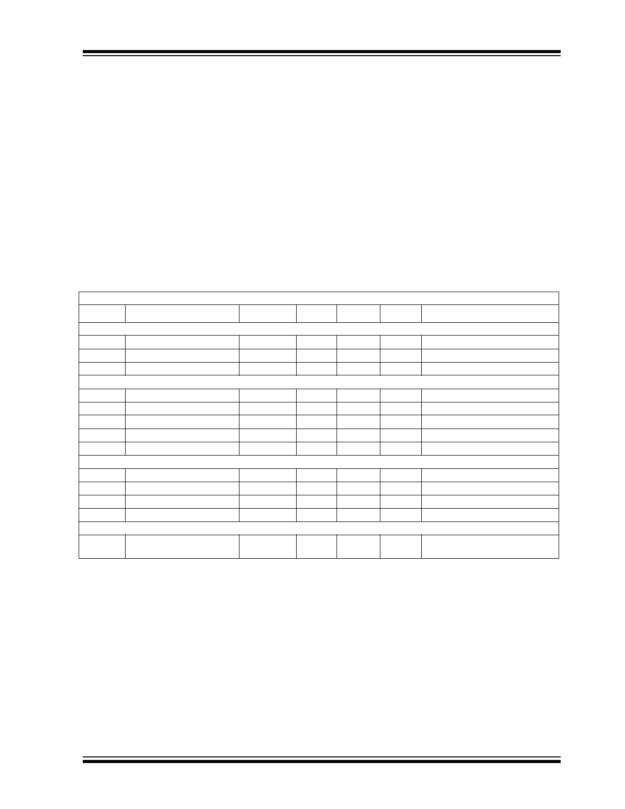
TC4403 ELECTRICAL SPECIFICATIONS
Electrical Characteristics: T
A
= +25°C, with 4.5V
V
DD
18V, unless otherwise noted.
Symbol
Parameter
Min
Typ
Max
Units
Test Conditions
Input
V
IH
Logic 1, High Input Voltage
2.4
—
—
V
V
IL
Logic 0, Low Input Voltage
—
—
0.8
V
I
IN
Input Current
-1000
±10
±1000
nA
-5V
V
IN
V
DD
Output
V
OH
High Output Voltage
V
DD
– 0.025
—
—
V
V
OL
Low Output Voltage
—
—
0.025
V
R
OS
Sourcing Output Resistance
—
2.8
5
I
OUT
= 10mA, V
DD
= 18V
R
OG
Grounding Output Resistance
—
3.5
5
I
OUT
= -10mA, V
DD
= 18V
I
PK
Peak Output Current
—
1.5
—
A
Switching Time (Note 1)
t
R
Rise Time
—
23
35
nsec
Figure 3-1, C
L
= 1800pF
t
F
Fall Time
—
25
35
nsec
Figure 3-1, C
L
= 1800pF
t
D1
Delay Time
—
33
75
nsec
Figure 3-1, C
L
= 1800pF
t
D2
Delay Time
—
38
75
nsec
Figure 3-1, C
L
= 1800pF
Power Supply
I
S
Power Supply Current
—
—
1.5
0.15
2.5
0.25
mA
V
IN
= 3V (Both Inputs)
V
IN
= 0V (Both Inputs)
Note
1:
Switching times ensured by design.
TC4403
DS21417C-page 4
2002-2012 Microchip Technology Inc.
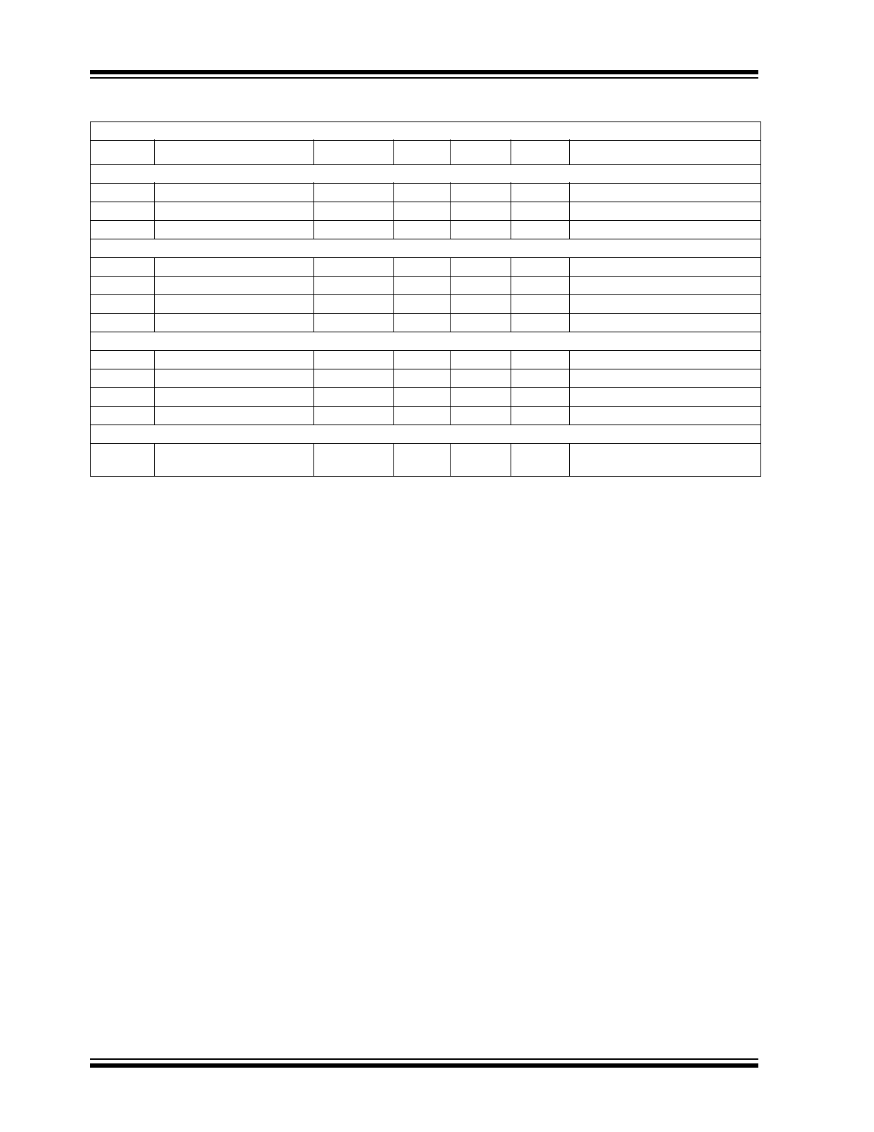
TC4403 ELECTRICAL SPECIFICATIONS (CONTINUED)
Electrical Characteristics: Over operating temperature range with 4.5V
V
DD
18V, unless otherwise noted.
Symbol
Parameter
Min
Typ
Max
Units
Test Conditions
Input
V
IH
Logic 1, High Input Voltage
2.4
—
—
V
V
IL
Logic 0, Low Input Voltage
—
—
0.8
V
I
IN
Input Current
-10,000
±10
±10,000
nA
-5V
V
IN
V
DD
Output
V
OH
High Output Voltage
V
DD
– 0.025
—
—
V
V
OL
Low Output Voltage
—
—
0.025
V
R
OS
Sourcing Output Resistance
—
3.7
8
V
IN
= 2.4V, I
OUT
= 10mA, V
DD
= 18V
R
OG
Grounding Output Resistance
—
4.3
8
V
IN
= 2.4V, I
OUT
= -10mA, V
DD
= 18V
Switching Time (Note 1)
t
R
Rise Time
—
28
60
nsec
Figure 3-1, C
L
= 1800pF
t
F
Fall Time
—
32
60
nsec
Figure 3-1, C
L
= 1800pF
t
D1
Delay Time
—
32
100
nsec
Figure 3-1, C
L
= 1800pF
t
D2
Delay Time
—
38
100
nsec
Figure 3-1, C
L
= 1800pF
Power Supply
I
S
Power Supply Current
—
—
2
0.2
3.5
0.3
mA
V
IN
= 3V (Both Inputs)
V
IN
= 0V (Both Inputs)
Note
1:
Switching times ensured by design.
2002-2012 Microchip Technology Inc.
DS21417C-page 5
TC4403
2.0
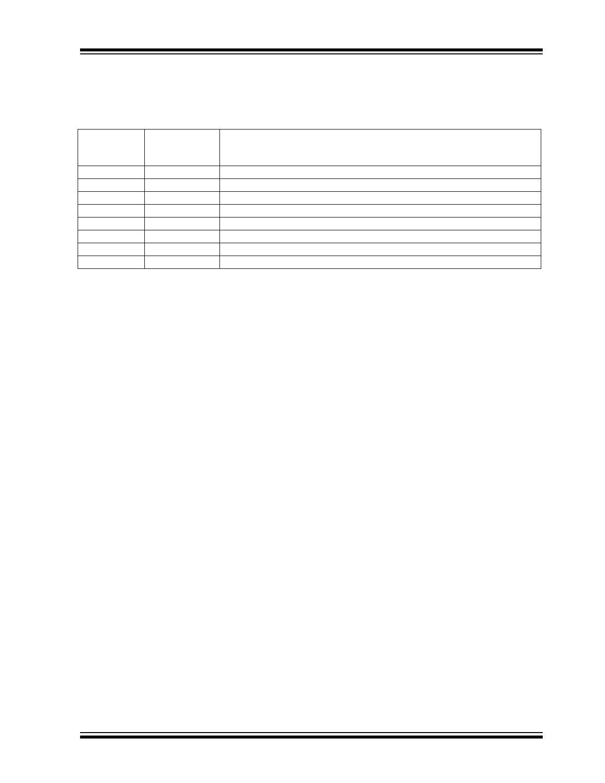
PIN DESCRIPTIONS
The descriptions of the pins are listed in Table 2-1.
TABLE 2-1:
PIN FUNCTION TABLE
Pin No.
(8-Pin PDIP,
CERDIP)
Symbol
Description
1
NC
No connection.
2
IN (V
DD
)
Control input V
DD
, TTL/CMOS compatible logic input signal, controls OUT (V
DD
).
3
GND
Ground.
4
IN (GND)
Control Input GND, TTL/CMOS compatible logic input signal, controls OUT (GND).
5
OUT (GND)
Output GND, CMOS Pull Down Output.
6
V
DD
Supply Input, 4.5V to 18V.
7
OUT (V
DD
)
Output V
DD
, CMOS pull-up output.
8
NC
No connection.
TC4403
DS21417C-page 6
2002-2012 Microchip Technology Inc.
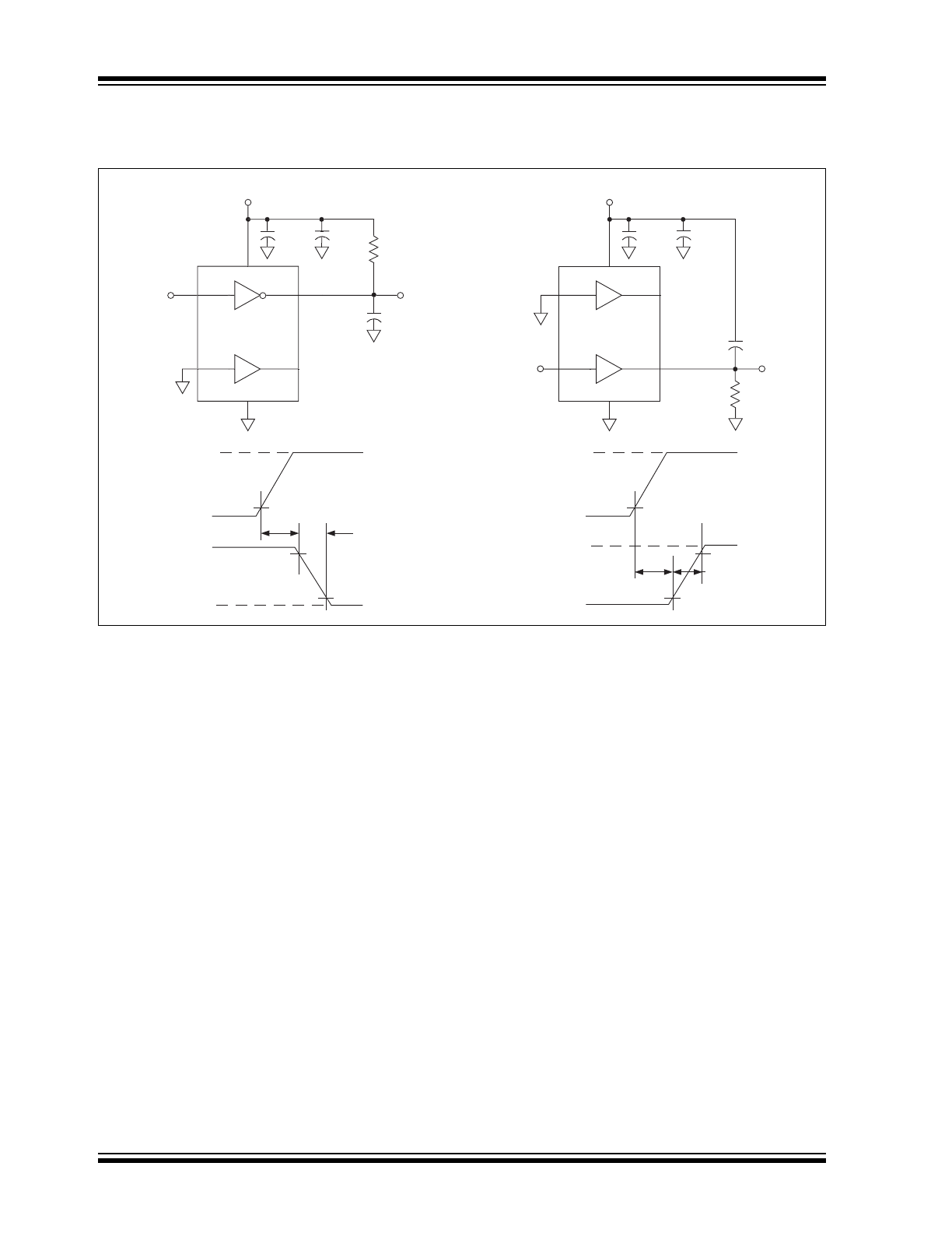
3.0
APPLICATIONS INFORMATION
FIGURE 3-1:
SWITCHING TIME TEST CIRCUITS
Input V
DD
Input GND
0.1
μF
MLC
1
μF
WIMA
MKS-2
10k
Ω
TC4403
0.1
μF
MLC
10K
Ω
TC4403
+5V
10%
90%
10%
16V
0V
10%
90%
10%
0V
1
μF
WIMA
MKS-2
Input V
DD
V
DD
= 16V
Input
Output
t
D1
t
F
C
L
= 1800pF
Output
t
R
+5V
16V
0V
0V
Input
Output
t
D1
C
L
= 1800pF
Output
V
DD
= 16V
Input GND
2002-2012 Microchip Technology Inc.
DS21417C-page 7
TC4403
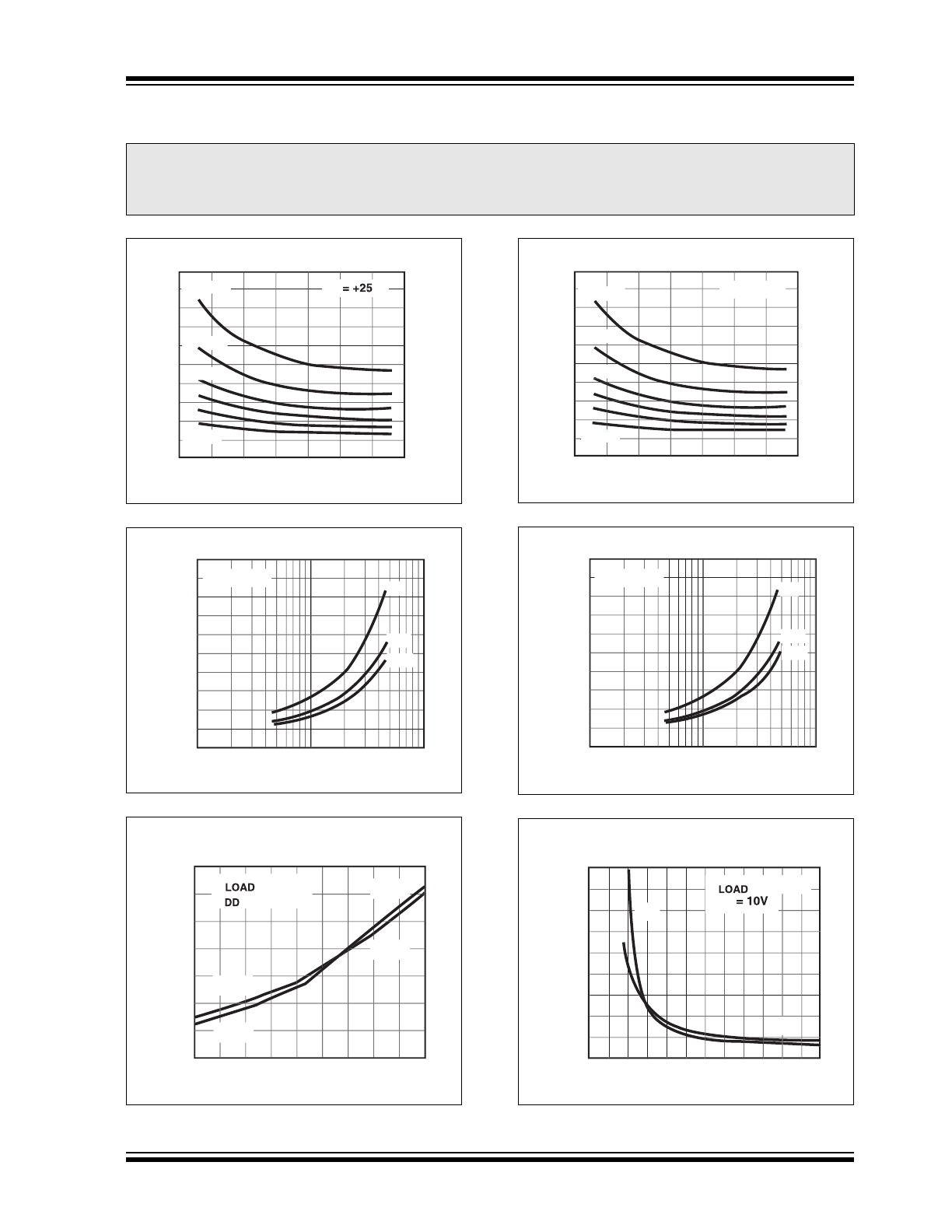
4.0
TYPICAL CHARACTERISTICS
Note:
The graphs and tables provided following this note are a statistical summary based on a limited number of
samples and are provided for informational purposes only. The performance characteristics listed herein are
not tested or guaranteed. In some graphs or tables, the data presented may be outside the specified
operating range (e.g., outside specified power supply range) and therefore outside the warranted range.
t
R
IS
E
(nsec
)
4
6
8
10
12
14
16
18
Rise Time vs. Supply Voltage
100
80
60
40
20
0
p
1000pF
p
p
4700pF
3300pF
470pF
p
1500pF
p
p
2200pF
T
A
°C
V
DD
(V)
Rise Time vs. Capacitive Load
100
1000
10,000
C
LOAD
(pF)
5V
10V
15V
100
80
60
40
20
0
T
A
= +25
°C
t
RISE
(nsec)
T
IME
(nsec
)
Rise and Fall Times vs.
Temperature
32
30
28
26
24
22
20
18
-55 -35
5
25
45
65
85 105 125
-15
TEMPERATURE (
°C)
t
FALL
t
RISE
t
FALL
t
RISE
C
= 2200pF
V
= 18V
t
FALL
(nsec)
4
6
8
10
12
14
16
18
Fall Time vs. Supply Voltage
100
80
60
40
20
0
p
1000pF
1500pF
p
p
p
4700pF
3300pF
p
p
2200pF
4
4
470pF
V
DD
(V)
T
A
= +25
°C
Fall Time vs. Capacitive Load
100
1000
10,000
5V
10V
15V
100
80
60
40
20
0
T
A
= +25
°C
t
FALL
(nsec)
C
LOAD
(pF)
Propagation Delay vs.
Input Amplitude
100
80
60
40
20
D
ELAY TIME
(nsec
)
INPUT (V)
0
1
2
3
4
5
6
7
8
9 10 11 12
t
D1
t
D2
C
= 2200pF
V
DD
TC4403
DS21417C-page 8
2002-2012 Microchip Technology Inc.
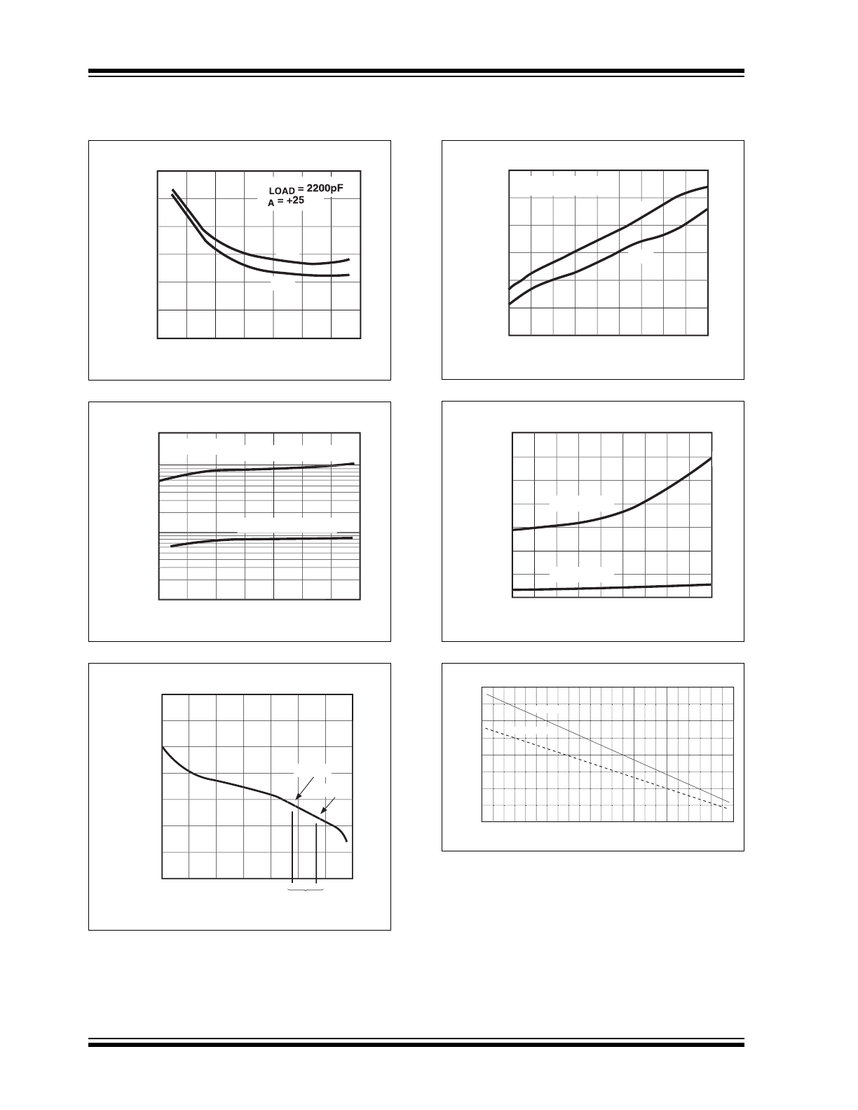
TYPICAL CHARACTERISTICS (CONTINUED)
Delay Time vs. Supply Voltage
50
45
40
35
30
25
20
4
6
8
10
12
14
16
18
DELAY TIME (nsec)
V
DD
(V)
C
T
°C
t
D1
t
D2
1
0.1
0.01
4
6
8
10
12
14
16
18
I
QUIESCENT
(mA)
Quiescent Current vs. Voltage
BOTH INPUTS = 1
BOTH INPUTS = 0
V
DD
(V)
T
A
= +25
°C
C
5.7
5.1
4.5
3.9
3.3
2.7
2.1
0
1.5
75
150
225
300
75 HOURS
525
2.768V
C
L
OS
ED
C
IR
CU
IT V
O
LTA
G
E
HOURS OF SERVICE
+
+
2.727V
Typical Discharge Characteristics
+
+
Delay Time vs. Temperature
50
45
40
35
30
25
20
DELAY TIME (ns)
-55 -35 -15
5
25
45
65
85 105 125
TEMPERATURE (
°C)
C
C
LOAD
= 2200pF
t
D1
t
D2
-55 -35 -15
5
25
45
65
85 105 125
Quiescent Current vs. Temperature
1.4
1.2
1.0
0.8
0.6
0.4
0.2
0.0
INPUTS = 1
INPUTS = 0
TEMPERATURE (
°C)
I
QUIESCENT
(mA)
200
0
400
600
800
1000
1200
1400
1600
0
10
20
30
40
50
60
70
80
90
100
110
120
AMBIENT TEMPERATURE (
°C)
MAX. POWER (mW)
8 Pin DIP
Thermal Derating Curves
8
8 Pin CERDIP
2002-2012 Microchip Technology Inc.
DS21417C-page 9
TC4403
5.0
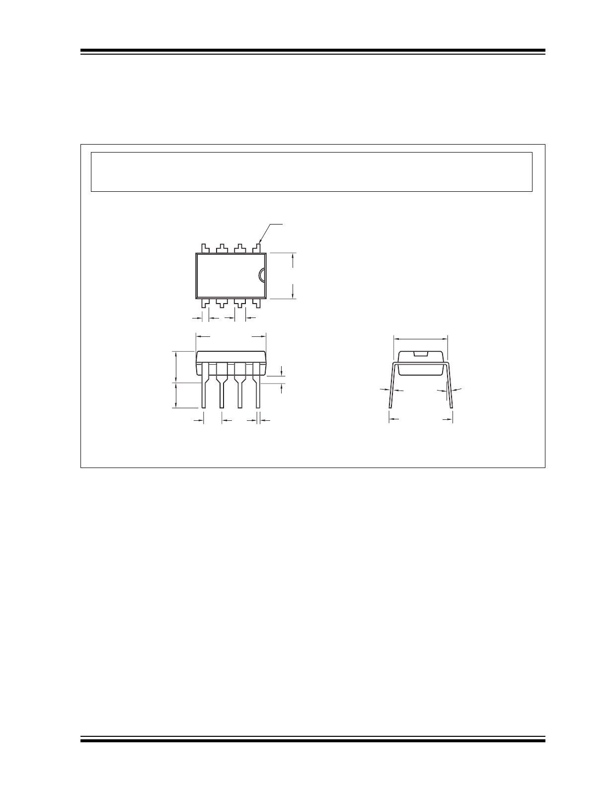
PACKAGING INFORMATION
5.1
Package Marking Information
Package marking data not available at this time.
5.2
Package Dimensions
3
° MIN.
PIN 1
.260 (6.60)
.240 (6.10)
.045 (1.14)
.030 (0.76)
.070 (1.78)
.040 (1.02)
.400 (10.16)
.348 (8.84)
.200 (5.08)
.140 (3.56)
.150 (3.81)
.115 (2.92)
.110 (2.79)
.090 (2.29)
.022 (0.56)
.015 (0.38)
.040 (1.02)
.020 (0.51)
.015 (0.38)
.008 (0.20)
.310 (7.87)
.290 (7.37)
.400 (10.16)
.310 (7.87)
8-Pin Plastic DIP
Dimensions: inches (mm)
Note:
For the most current package drawings, please see the Microchip Packaging Specification located
at http://www.microchip.com/packaging
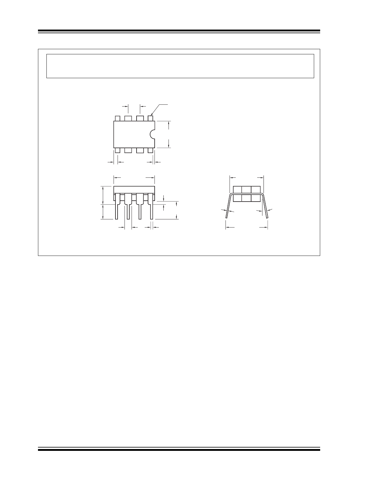
TC4403
DS21417C-page 10
2002-2012 Microchip Technology Inc.
.400 (10.16)
.370 (9.40)
.300 (7.62)
.230 (5.84)
.065 (1.65)
.045 (1.14)
.055 (1.40) MAX.
.020 (0.51) MIN.
PIN 1
.200 (5.08)
.160 (4.06)
.200 (5.08)
.125 (3.18)
.110 (2.79)
.090 (2.29)
.020 (0.51)
.016 (0.41)
.040 (1.02)
.020 (0.51)
.320 (8.13)
.290 (7.37)
.150 (3.81)
MIN.
3
° MIN.
8-Pin CERDIP (Narrow)
.015 (0.38)
.008 (0.20)
.400 (10.16)
.320 (8.13)
Dimensions: inches (mm)
Note:
For the most current package drawings, please see the Microchip Packaging Specification located
at http://www.microchip.com/packaging