
2017 Microchip Technology Inc.
DS20005537B-page 1
DN2625
Features
• Very Low Gate Threshold Voltage
• Designed to be Source-driven
• Low Switching Losses
• Low Effective Output Capacitance
• Designed for Inductive Loads
Applications
• Medical Ultrasound Beamforming
• Ultrasonic Array-focusing Transmitter
• Piezoelectric Transducer Waveform Drivers
• High-speed Arbitrary Waveform Generator
• Normally-on Switches
• Solid-state Relays
• Constant Current Sources
• Power Supply Circuits
General Description
The DN2625 is a low-threshold Depletion-mode
(normally-on) transistor that utilizes an advanced
vertical DMOS structure and a well-proven silicon gate
manufacturing process. This combination produces a
device with the power handling capabilities of bipolar
transistors as well as the high input impedance and
positive temperature coefficient inherent in
Metal-Oxide Semiconductor (MOS) devices.
Characteristic of all MOS structures, this device is free
from thermal runaway and thermally induced
secondary breakdown.
Vertical DMOS Field-Effect Transistors (FETs) are ide-
ally suited to a wide range of switching and amplifying
applications where high breakdown voltage, high input
impedance, low input capacitance and fast switching
speeds are desired.
The DN2625DK6-G contains two MOSFETs in an
8-lead, dual-pad DFN package. The DN2625 contains
a single MOSFET in a TO-252 D-PAK package.
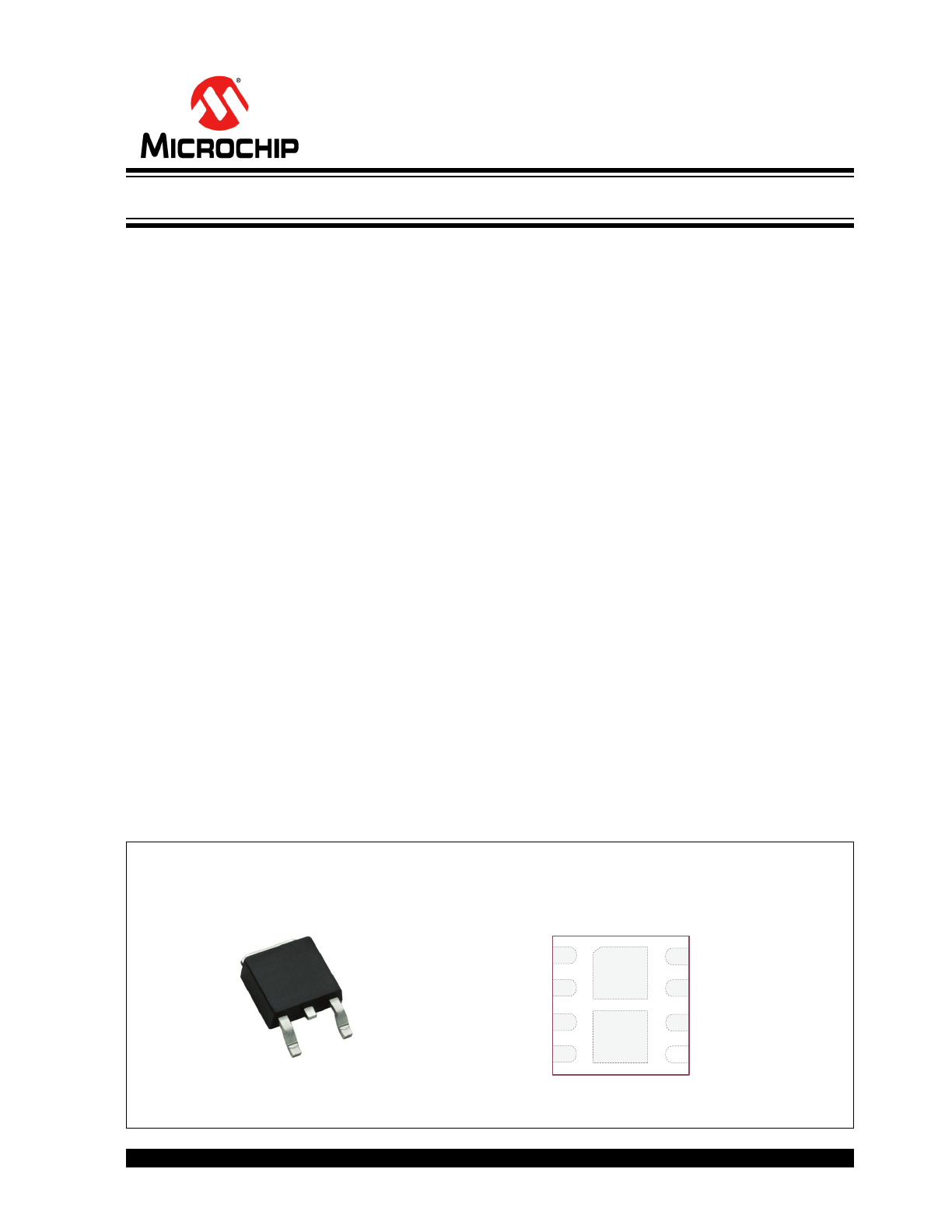
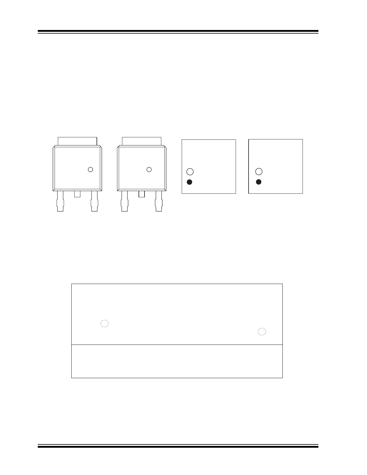
Package Types
TO-252 D-PAK
(Top view)
GATE
SOURCE
DRAIN
See
Table 3-1
and
Table 3-2
for pin information.
8
1
2
3
4
7
6
5
S1
G1
D1
S2
G2
D1
D2
D2
D1
D2
8-lead DFN (Dual Pad)
(Top view)
N-Channel Depletion-Mode Vertical DMOS FET in Single and Dual Options
DN2625
DS20005537B-page 2
2017 Microchip Technology Inc.
1.0
ELECTRICAL CHARACTERISTICS
Absolute Maximum Ratings†
Drain-to-source Voltage ....................................................................................................................................... BV
DSX
Drain-to-gate Voltage .......................................................................................................................................... BV
DGX
Gate-to-source Voltage ......................................................................................................................................... ±20V
Operating Ambient Temperature, T
A
..................................................................................................... –55°C to 150°C
Storage Temperature, T
S
....................................................................................................................... –55°C to 150°C
Soldering Temperature (
Note 1
) ........................................................................................................................... 300°C
† Notice: Stresses above those listed under “Absolute Maximum Ratings” may cause permanent damage to the
device. This is a stress rating only, and functional operation of the device at those or any other conditions above those
indicated in the operational sections of this specification is not intended. Exposure to maximum rating conditions for
extended periods may affect device reliability.
Note 1: Distance of 1.6 mm from case for 10 seconds
DC ELECTRICAL CHARACTERISTICS
Electrical Specifications: Unless otherwise noted, T
A
= 25°C. (
Note 1
)
Parameter
Sym.
Min.
Typ.
Max.
Unit
Conditions
Drain-to-source Breakdown Voltage
BV
DSX
250
—
—
V
V
GS
= –2.5V, I
D
= 50 µA
Drain-to-gate Breakdown Voltage
BV
DGX
250
—
—
V
V
GS
= –2.5V, I
D
= 50 µA
Gate-to-source Off Voltage
V
GS(OFF)
–1.5
—
–2.1
V
V
DS
= 15V, I
D
= 100 µA
Change in V
GS(OFF)
with Temperature
∆V
GS(OFF)
—
—
–4.5
mV/°C V
DS
= 15V, I
D
= 100 µA (
Note 2
)
Gate Body Leakage Current
I
GSS
—
—
100
nA
V
GS
= ±20V, V
DS
= 0V
Drain-to-source Leakage Current
I
D(OFF)
—
—
1
µA
V
DS
= 250V, V
GS
= –5V
—
—
200
V
DS
= 250V, V
GS
= –5V,
T
A
= 125°C (
Note 2
)
Saturated Drain-to-source Current
I
DSS
1.1
—
—
A
V
GS
= 0V, V
DS
= 15V
Pulsed Drain-to-source Current
I
DS(PULSE)
3.1
3.3
—
A
V
GS
= 0.9V, V
DS
= 15V
(With duty cycle of 1%)
Static Drain-to-source On-resistance
R
DS(ON)
—
—
3.5
Ω
V
GS
= 0V, I
D
= 1A
Change in R
DS(ON)
with
Temperature
∆
RDS(ON)
—
—
1.1
%/°C
V
GS
= –0V, I
D
= 200 mA (
Note 2
)
Note 1: Unless otherwise stated, all DC parameters are 100% tested at +25°C. Pulse test: 300 µs pulse, 2% duty
cycle.
2: Specification is obtained by characterization and is not 100% tested.
AC ELECTRICAL CHARACTERISTICS
Electrical Specifications: Unless otherwise noted, T
A
= 25°C. (
Note 2
)
Parameter
Sym.
Min.
Typ.
Max.
Unit
Conditions
Forward Transconductance
G
FS
100
—
—
mmh0 V
DS
= 10V, I
D
= 150 mA
Input Capacitance
C
ISS
—
800
1000
pF
V
GS
= –2.5V,
V
DS
= 25V,
f = 1 MHz
Common Source Output Capacitance
C
OSS
—
70
210
pF
Reverse Transfer Capacitance
C
RSS
—
18
70
pF
Turn-on Delay Time
t
d(ON)
—
—
10
ns
V
DD
= 25V,
I
D
= 150 mA,
R
GEN
= 3Ω,
V
GS
= 0V to –10V
Rise Time
t
r
—
—
20
ns
Turn-off Delay Time
t
d(OFF)
—
—
10
ns
Fall Time
t
f
—
—
20
ns
Total Gate Charge
Q
G
—
—
7.04
nC
I
D
= 3.5A,
V
DS
= 100V,
V
GS
= 1.5V
Gate-to-source Charge
Q
GS
—
—
0.783
nC
Gate-to-drain Charge
Q
GD
—
—
3.73
nC
DIODE PARAMETER
Diode Forward Voltage Drop
V
SD
—
—
1.8
V
V
GS
= –2.5V, I
SD
= 150 mA
(
Note 1
)
Note 1: Unless otherwise stated, all DC parameters are 100% tested at +25°C. Pulse test: 300 µs pulse, 2% duty
cycle.
2: Specification is obtained by characterization and is not 100% tested.
TEMPERATURE SPECIFICATIONS
Electrical Specifications: Unless otherwise specified, for all specifications T
A
= T
J
= +25°C.
Parameter
Sym.
Min.
Typ.
Max.
Unit
Conditions
TEMPERATURE RANGE
Operating Ambient Temperature
T
A
–55
—
150
°C
Storage Temperature
T
S
–55
—
150
°C
Soldering Temperature
—
—
—
300
°C
Note 1
PACKAGE THERMAL RESISTANCE
TO-252 D-PAK
θ
JA
—
81
—
°C/W
Note 2
8-lead DFN (Dual Pad)
θ
JA
—
29
—
°C/W
Note 3
Note 1: Distance of 1.6 mm from case for 10 seconds
2: Four-layer, 1-oz, 3 x 4-inch PCB with 20 via for drain pad
3: Four-layer, 1-oz, 3 x 4-inch PCB with 12 via for drain pad
THERMAL CHARACTERISTICS
Package
I
D
(
1
)
(Continuous)
(A)
I
D
(Pulsed)
(A)
I
DR
(
1
)
(A)
I
DRM
(A)
TO-252 D-PAK
1.1
3.3
1.1
3.3
8-lead DFN (Dual Pad)
1.1
3.3
1.1
3.3
Note 1:
I
D
(Continuous) is limited by maximum T
J
.
2017 Microchip Technology Inc.
DS20005537B-page 3
DN2625
DN2625
DS20005537B-page 4
2017 Microchip Technology Inc.
2.0
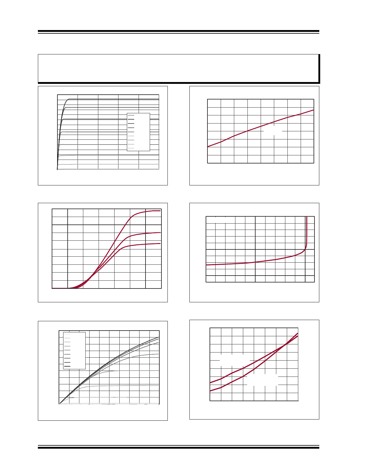
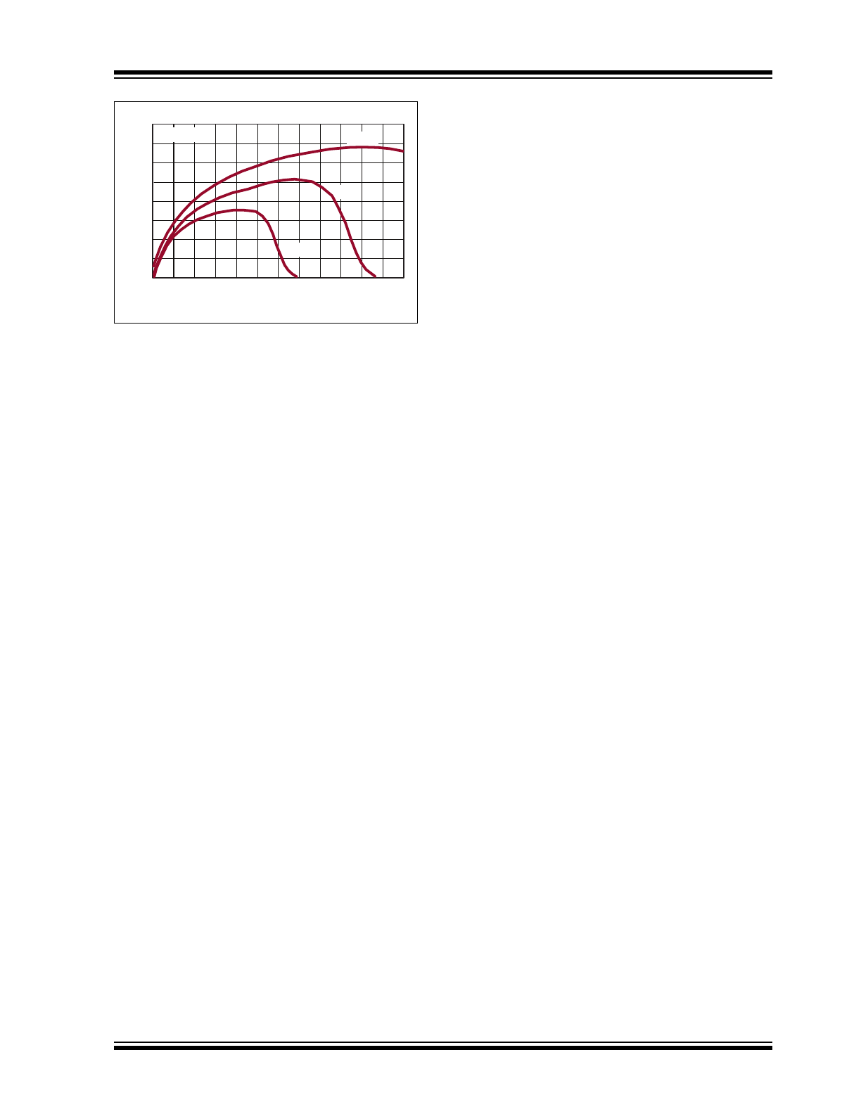
TYPICAL PERFORMANCE CURVES
0.0
1.0
2.0
3.0
4.0
5.0
6.0
7.0
0
50
100
150
200
250
V
DS
(volts)
I
D
(amps)
V
GS
= 2.0V
V
GS
= 1.5V
V
GS
= 1.0V
V
GS
= 0.5V
V
GS
= 0V
V
GS
= -0.5V
V
GS
= -1.0V
V
GS
= -1.5V
V
GS
= -2.0V
Note:
The graphs and tables provided following this note are a statistical summary based on a limited number of
samples and are provided for informational purposes only. The performance characteristics listed herein
are not tested or guaranteed. In some graphs or tables, the data presented may be outside the specified
operating range (e.g. outside specified power supply range) and therefore outside the warranted range.
FIGURE 2-1:
Output Characteristics.
0
1
2
3
4
5
6
7
8
9
10
-3.0
-2.0
-1.0
0.0
1.0
2.0
3.0
4.0
V
GS
(V)
I
D
(amps)
-55
O
C
25
O
C
125
O
C
FIGURE 2-2:
Transfer Characteristics.
0.0
0.5
1.0
1.5
2.0
2.5
3.0
3.5
4.0
4.5
5.0
5.5
0
1
2
3
4
5
6
7
8
9
10
V
DS
(V)
I
D
(A)
V
GS
= -2V
V
GS
= -1.5V
V
GS
= -1V
V
GS
= -0.5V
V
GS
= 0V
V
GS
= 0.5V
V
GS
= 1V
V
GS
= 1.5V
V
GS
= 2V
FIGURE 2-3:
Saturation Characteristics.
FIGURE 2-4:
BV
DSX
Variation with
Temperature.
0.80
0.85
0.90
0.95
1.00
1.05
1.10
1.15
1.20
-50
-25
0
25
50
75
100
125
150
T
j
(
O
C)
BV
DSX
(normalized)
V
GS
= -2.5V
I
D
= 1mA
0.0
0.5
1.0
1.5
2.0
2.5
3.0
3.5
4.0
4.5
5.0
0.0
0.5
1.0
1.5
2.0
2.5
3.0
3.5
4.0
4.5
5.0
5.5
I
D
(A)
R
DS(ON)
(ohms)
V
GS
= 1V
FIGURE 2-5:
On-resistance vs. Drain
Current.
0.80
0.85
0.90
0.95
1.00
1.05
1.10
1.15
1.20
1.25
-50 -25 0 25 50 75 100 125 150
T
j
(
O
C)
V
GS(OFF)
(normalized)
0.25
0.50
0.75
1.00
1.25
1.50
1.75
2.00
2.25
2.50
V
GS(OFF)
@100µA
V
DS
= 15V
R
DS(ON)
@V
GS
= 1V
I
D
=1A
R
DS(ON)
(normalized)
FIGURE 2-6:
V
GS(OFF)
and R
DS(ON)
Variation with Temperature.
2017 Microchip Technology Inc.
DS20005537B-page 5
DN2625
FIGURE 2-7:
Transconductance vs. Drain
Current.
0.0
0.5
1.0
1.5
2.0
2.5
3.0
3.5
4.0
0.0
0.5
1.0
1.5
2.0
2.5
3.0
3.5
4.0
4.5
5.0
5.5
6.0
I
D
(A)
G
FS
(Siemens)
-55
O
C
25
O
C
125
O
C
V
DS
= 10V
DN2625
DS20005537B-page 6
2017 Microchip Technology Inc.
3.0
PIN DESCRIPTION
The details on the pins of TO-252 D-PAK and 8-lead
DFN (dual pad) are listed in
Table 3-1
and
Table 3-2
.
Refer to
Package Types
for the location of pins.
TABLE 3-1:
TO-252 D-PAK PIN FUNCTION TABLE
Pin Number
Pin Name
Description
1
Gate
Gate
2
Drain
Drain
3
Source
Source
4
Drain
Drain
TABLE 3-2:
8-LEAD DFN (DUAL PAD) PIN FUNCTION TABLE
Pin Number
Pin Name
Description
1
S1
Device 1 source
2
G1
Device 1 gate
3
S2
Device 2 source
4
G2
Device 2 gate
5
D2
Device 2 drain
6
D2
Device 2 drain
7
D1
Device 1 drain
8
D1
Device 1 drain
2017 Microchip Technology Inc.
DS20005537B-page 7
DN2625
4.0
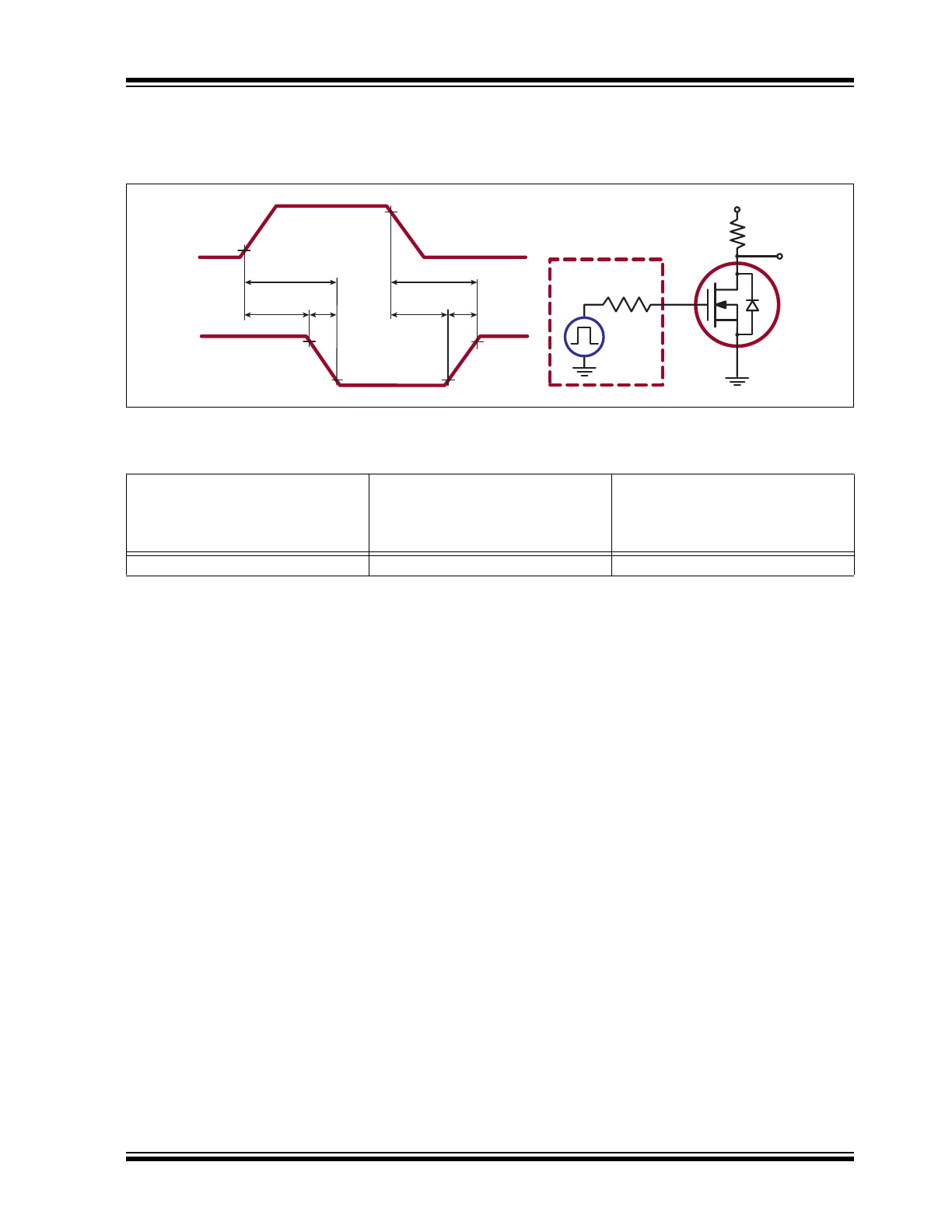
FUNCTIONAL DESCRIPTION
Figure 4-1
shows the switching waveforms and test
circuit for DN2625.
90%
10%
90%
90%
10%
10%
Pulse
Generator
VDD
R
L
OUTPUT
D.U.T.
t
(ON)
t
d(ON)
t
(OFF)
t
d(OFF)
t
r
INPUT
INPUT
OUTPUT
0V
VDD
R
GEN
0V
-10V
t
f
FIGURE 4-1:
Switching Waveforms and Test Circuit.
PRODUCT SUMMARY
BV
DSX
/BV
DGX
(V)
V
GS(OFF)
(Maximum)
(V)
I
DS
(Pulsed)
(V
GS
= 0.9V)
(Minimum)
(A)
250
–2.1
3.3
DN2625
DS20005537B-page 8
2017 Microchip Technology Inc.
5.0
PACKAGING INFORMATION
5.1
Package Marking Information
Legend: XX...X
Product Code or Customer-specific information
Y
Year code (last digit of calendar year)
YY
Year code (last 2 digits of calendar year)
WW
Week code (week of January 1 is week ‘01’)
NNN
Alphanumeric traceability code
Pb-free JEDEC
®
designator for Matte Tin (Sn)
*
This package is Pb-free. The Pb-free JEDEC designator ( )
can be found on the outer packaging for this package.
Note:
In the event the full Microchip part number cannot be marked on one line, it will
be carried over to the next line, thus limiting the number of available
characters for product code or customer-specific information. Package may or
not include the corporate logo.
3
e
3
e
TO-252 (D-PAK)
Example
YYWWNNN
XXXXX
XXXX
e3
1641343
2625
DN
e3
8-lead DFN
Example
NNN
XXXXXXX
XXXXXXX
YYWW
e3
343
K6
DN2625D
1613
e3
2017 Microchip Technology Inc.
DS20005537B-page 9
DN2625
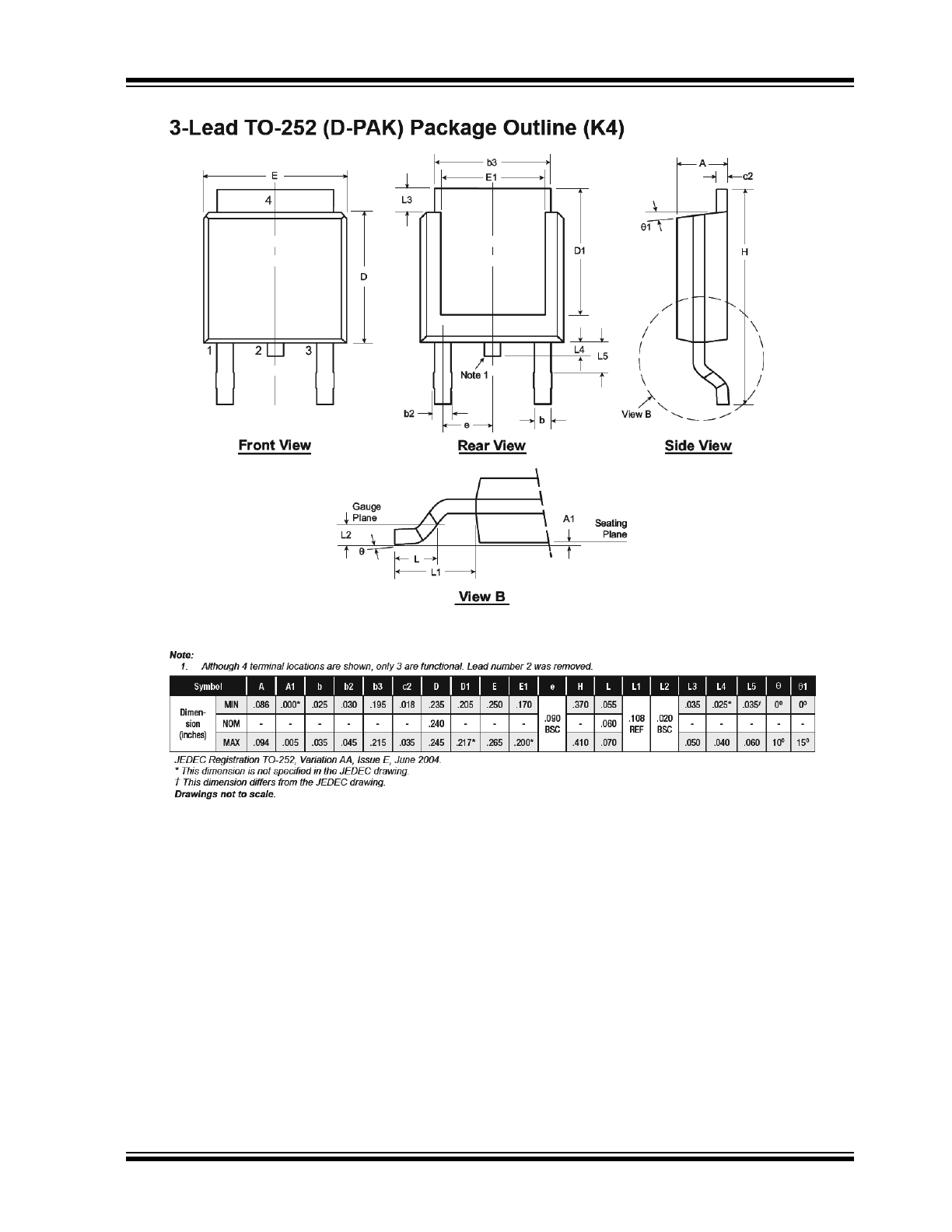
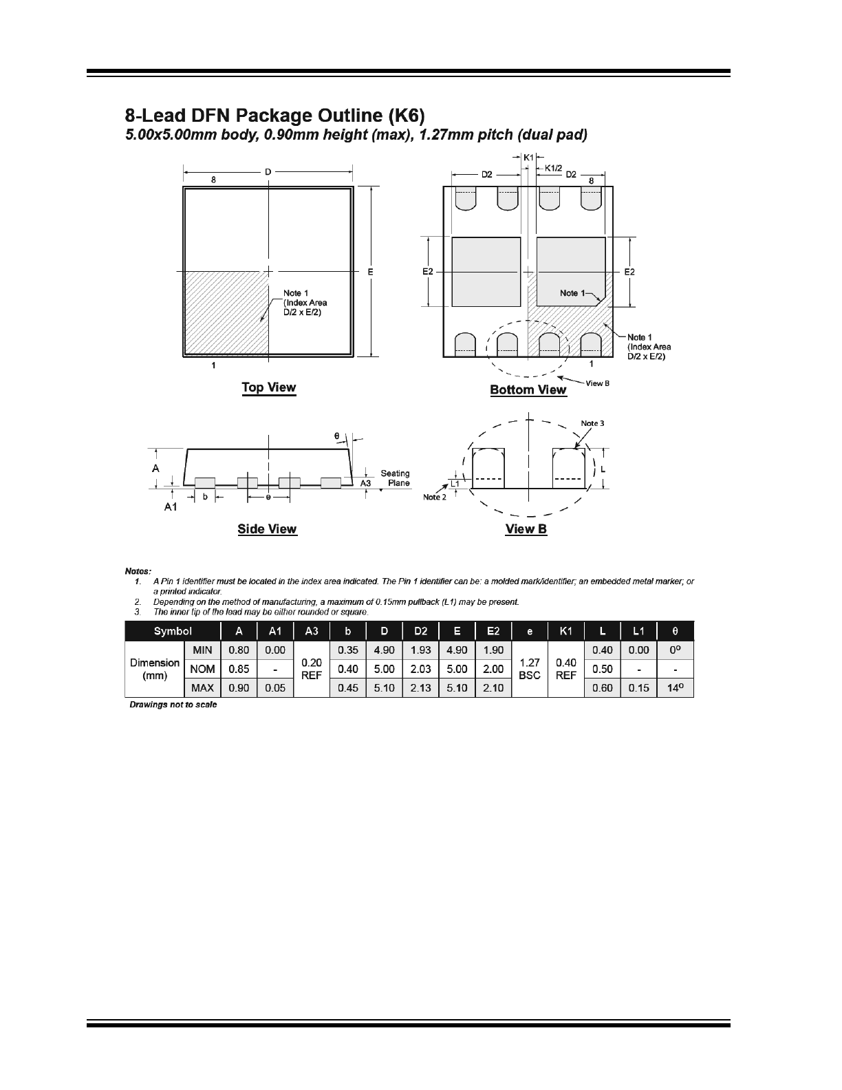
Note: For the most current package drawings, see the Microchip Packaging Specification at www.microchip.com/packaging.
DN2625
DS20005537B-page 10
2017 Microchip Technology Inc.
Note: For the most current package drawings, see the Microchip Packaging Specification at www.microchip.com/packaging.