
© 2011 Microchip Technology Inc.
DS21743B-page 1
TC72
Features
• Temperature-to-Digital Converter
• SPI Compatible Interface
• 10-Bit Resolution (0.25°C/Bit)
• ±2°C (maximum) Accuracy from -40°C to +85°C
• ±3°C (maximum) Accuracy from -55°C to +125°C
• 2.65V to 5.5V Operating Range
• Low Power Consumption:
- 250 µA (typical) Continuous Temperature
Conversion Mode
- 1 µA (maximum) Shutdown Mode
• Power Saving One-Shot Temperature
Measurement
• Industry Standard 8-Pin MSOP Package
• Space Saving 8-Pin DFN (3x3 mm) Package
Typical Applications
• Personal Computers and Servers
• Hard Disk Drives and Other PC Peripherals
• Entertainment Systems
• Office Equipment
• Datacom Equipment
• Mobile Phones
• General Purpose Temperature Monitoring
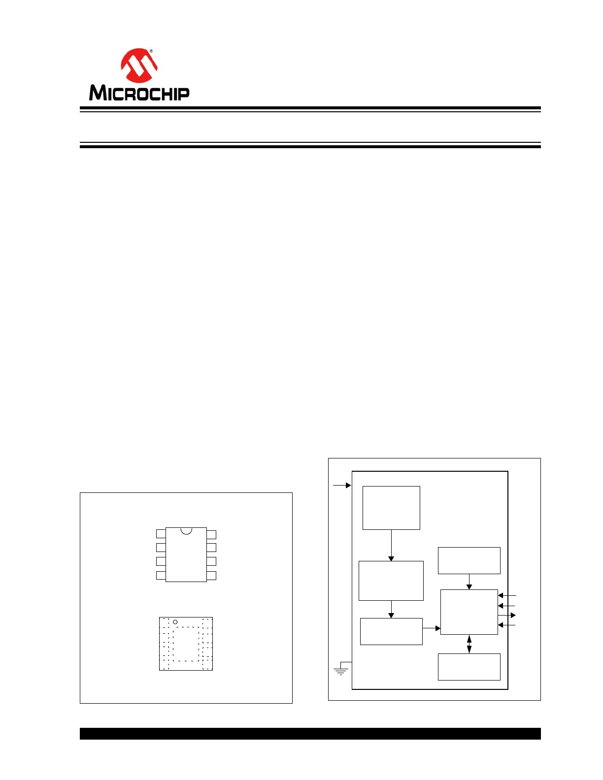
Package Types
General Description
TC72 is a digital temperature sensor capable of
reading temperatures from -55°C to +125°C. This
sensor features a serial interface that allows
communication with a host controller or other
peripherals. The TC72 interface is compatible with the
SPI protocol, and does not require any additional
external components. However, it is recommended that
a decoupling capacitor of 0.01 µF to 0.1 µF be provided
between the V
DD
and GND pins.
TC72 can be used either in a Continuous Temperature
Conversion mode or a One-Shot Conversion mode.
The Continuous Conversion mode measures the
temperature approximately every 150 ms and stores
the data in the temperature registers. In contrast, the
One-Shot mode performs a single temperature
measurement and returns to the power saving
shutdown mode.
TC72 features high temperature accuracy, ease-of-use
and is the ideal solution for implementing thermal
management in a variety of systems. The device is
available in both 8-pin MSOP and 8-pin DFN space-
saving packages. TC72 also features a Shutdown
mode for low power operation.
Block Diagram
SCK
CE
GND
NC
SDI
1
2
3
4
8
7
6
5 SDO
V
DD
NC
TC72
3x3 DFN*
CE
SCK
GND
NC
SDO
1
2
3
4
8
7
6
5 SDI
V
DD
NC
EP
9
* Includes Exposed Thermal Pad (EP); see
Table 3-1
.
TC72
MSOP
TC72
Diode
Temperature
Sensor
V
DD
SCK
CE
Serial
Port
Interface
10-Bit
Sigma Delta
A/D Converter
Register
Temperature
Register
Internal
Control
Manufacturer
ID Register
GND
SDO
SDI
Digital Temperature Sensor with SPI
Interfa
ce

TC72
DS21743B-page 2
© 2011 Microchip Technology Inc.
NOTES:
© 2011 Microchip Technology Inc.
DS21743B-page 3
TC72
1.0
ELECTRICAL
CHARACTERISTICS
1.1
Maximum Ratings
†
V
DD
........................................................................ 6.0V
All inputs and outputs w.r.t. GND ...-0.3V to V
DD
+0.3V
Storage temperature .......................... -65°C to +150°C
Ambient temp. with power applied ..... -55°C to +125°C
Junction Temperature ........................................ 150°C
ESD protection on all pins:
Human Body Model (HBM)............................. > 4 kV
Man Machine Model (MM)............................. > 400V
Latch-Up Current at each pin ........................ ±200 mA
Maximum Power Dissipation........................... 250 mW
† Notice: Stresses above those listed under "Maximum
Ratings" may cause permanent damage to the device. This is
a stress rating only and functional operation of the device at
those or any other conditions above those indicated in the
operation listings of this specification is not implied. Exposure
to maximum rating conditions for extended periods may affect
device reliability.
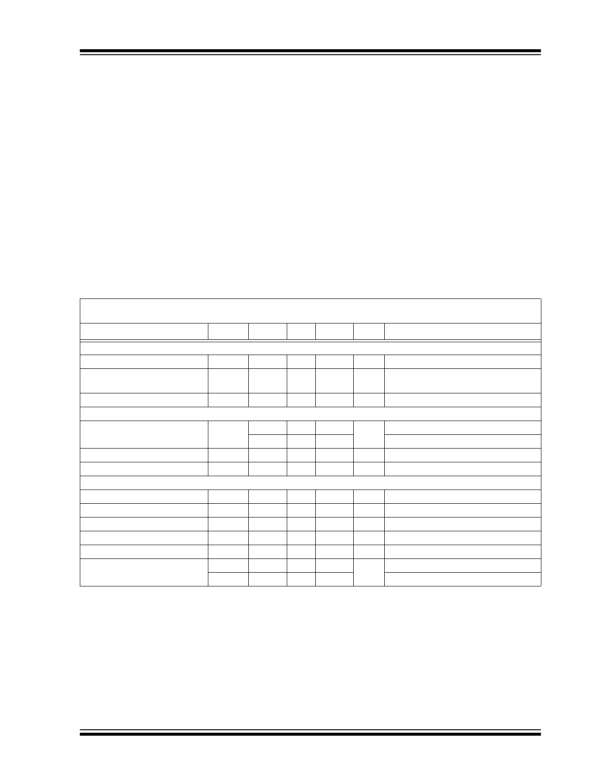
DC CHARACTERISTICS
Electrical Specifications: Unless otherwise noted, all parameters apply at V
DD
= 2.65V to 5.5V,
T
A
= -55°C to +125°C.
Parameters
Sym
Min
Typ
Max
Units
Conditions
Power Supply
Operating Voltage Range
V
DD
2.65
—
5.5
V
Note 1
Operating Current:
Normal Mode, ADC Active
I
DD-CON
—
250
400
µA
Continuous Temperature Conversion
mode (Shutdown Bit = ‘0’)
Shut-Down Supply Current
I
SHD
—
0.1
1.0
µA
Shutdown mode (Shutdown Bit = ‘1’)
Temperature Sensor and Analog-to-Digital Converter
Temperature Accuracy
(
Note 1
)
T
ACY
-2.0
—
+2.0
°C
-40°C < T
A
< +85°C
-3.0
—
+3.0
-55°C < T
A
< +125°C
Resolution
—
10
—
Bits
Note 4
ADC Conversion Time
t
CONV
—
150
200
ms
Digital Input / Output
High Level Input Voltage
V
IH
0.7 V
DD
—
—
V
Low Level Input Voltage
V
IL
—
—
0.2 V
DD
V
High Level Output Voltage
V
OH
0.7 V
DD
—
—
V
I
OH
= 1 mA
Low Level Output Voltage
V
OL
—
—
0.2 V
DD
V
I
OL
= 4 mA
Input Resistance
R
IN
1.0
—
—
M
Ω
Pin Capacitance
C
IN
—
15
—
pF
C
OUT
—
50
—
Note 1:
The TC72-2.8MXX, TC72-3.3MXX and TC72-5.0MXX will operate from a supply voltage of 2.65V to 5.5V.
However, the TC72-2.8MXX, TC72-3.3MXX and TC72-5.0MXX are tested and specified at the nominal
operating voltages of 2.8V, 3.3V and 5.0V respectively. As V
DD
varies from the nominal operating value,
the accuracy may be degraded. Refer to
Figure 2-5
and
Figure 2-6
.
2:
Measured with a load of C
L
= 50 pF on the SDO output pin of the TC72.
3:
All time measurements are measured with respect to the 50% point of the signal, except for the SCK rise
and fall times. The rise and fall times are defined as the 10% to 90% transition time.
4:
Resolution = Temperature Range/No. of Bits = (+127°C – -128°C) / (2
10
) = 256/1024 = 0.25°C/Bit
TC72
DS21743B-page 4
© 2011 Microchip Technology Inc.
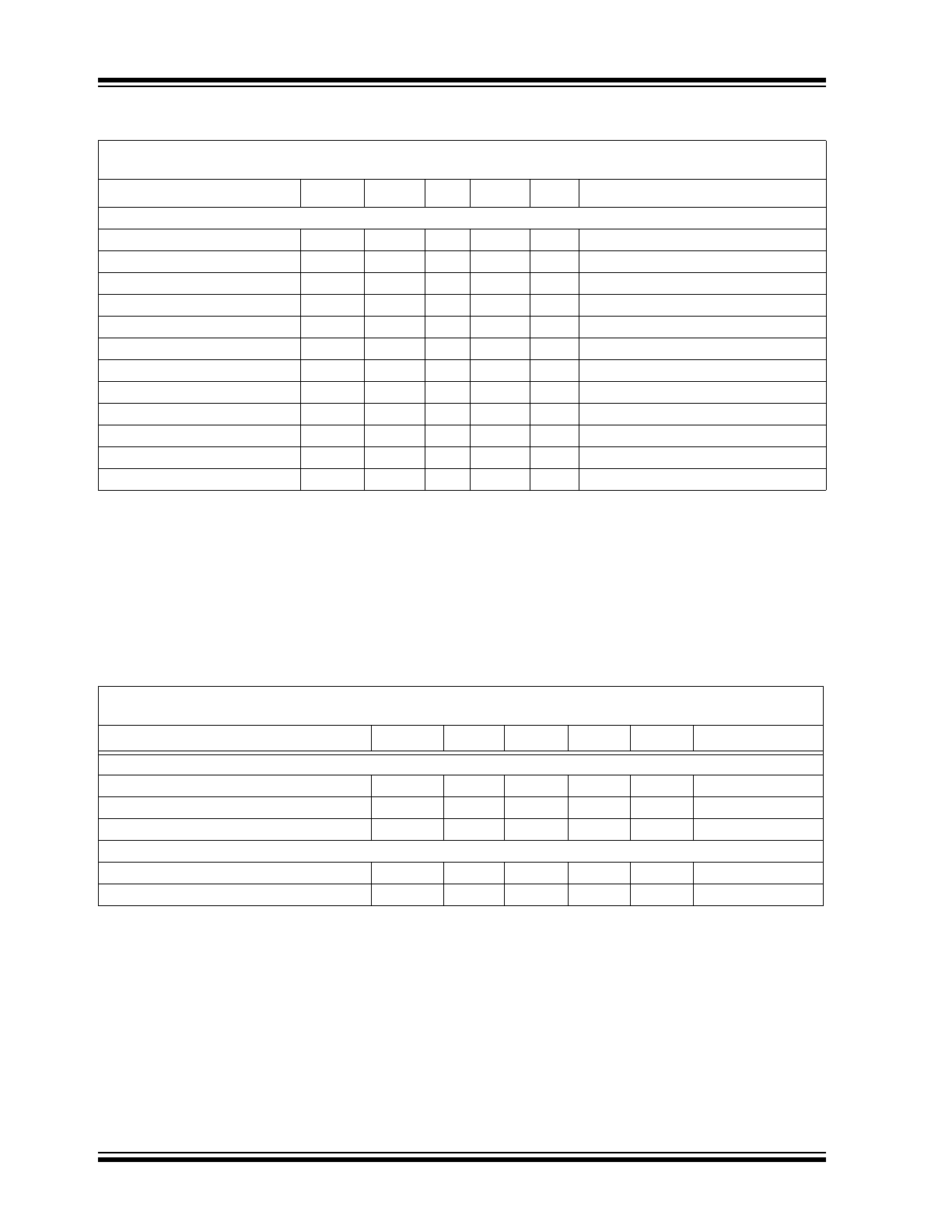
Serial Port AC Timing (
Note 2
,
3
)
Clock Frequency
f
CLK
DC
—
7.5
MHz
SCK Low Time
t
CL
65
—
—
ns
SCK High Time
t
CH
65
—
—
ns
CE to SCK Setup
t
CC
400
—
—
ns
SCK to Data Out Valid
t
CDD
—
—
55
ns
CE to Output Tri-state
t
CDZ
—
—
40
ns
SCK to Data Hold Time
t
CDH
35
—
—
ns
Data to SCK Set-up Time
t
DC
35
—
—
ns
SCK to CE Hold Time
t
CCH
100
—
—
ns
SCK Rise Time
t
R
—
—
200
ns
SCK Fall Time
t
F
—
—
200
ns
CE Inactive Time
t
CWH
400
—
—
ns
TEMPERATURE SPECIFICATION
Electrical Specifications: Unless otherwise noted, all parameters apply at V
DD
= 2.65V to 5.5V,
T
A
= -55°C to +125°C.
Parameters
Sym
Min
Typ
Max
Units
Conditions
Temperature Ranges
Specified Temperature Range
T
A
-55
—
+125
°C
Operating Temperature Range
T
A
-55
—
+125
°C
Storage Temperature Range
T
A
-65
—
+150
°C
Thermal Package Resistances
Thermal Resistance 8-L 3x3 DFN
θ
JA
—
56.7
—
°C/W
Thermal Resistance 8-L MSOP
θ
JA
—
211
—
°C/W
DC CHARACTERISTICS (CONTINUED)
Electrical Specifications: Unless otherwise noted, all parameters apply at V
DD
= 2.65V to 5.5V,
T
A
= -55°C to +125°C.
Parameters
Sym
Min
Typ
Max
Units
Conditions
Note 1:
The TC72-2.8MXX, TC72-3.3MXX and TC72-5.0MXX will operate from a supply voltage of 2.65V to 5.5V.
However, the TC72-2.8MXX, TC72-3.3MXX and TC72-5.0MXX are tested and specified at the nominal
operating voltages of 2.8V, 3.3V and 5.0V respectively. As V
DD
varies from the nominal operating value,
the accuracy may be degraded. Refer to
Figure 2-5
and
Figure 2-6
.
2:
Measured with a load of C
L
= 50 pF on the SDO output pin of the TC72.
3:
All time measurements are measured with respect to the 50% point of the signal, except for the SCK rise
and fall times. The rise and fall times are defined as the 10% to 90% transition time.
4:
Resolution = Temperature Range/No. of Bits = (+127°C – -128°C) / (2
10
) = 256/1024 = 0.25°C/Bit
© 2011 Microchip Technology Inc.
DS21743B-page 5
TC72
FIGURE 1-1:
Serial Port Timing Diagrams.
CE
1/f
CLK
t
CL
t
CH
D7
D0
HIGH Z
SDI
SPI READ DATA TRANSFER
CE
1/f
CLK
t
CC
A7 = 1
t
CL
t
CH
D7
D0
SDI
A0
A7
t
DC
t
CDH
A0
t
F
t
R
t
DC
t
CDH
t
R
t
F
SCK
t
CC
(CP = 0, data shifted on rising edge of SCK, data clocked on falling edge of SCK, A7 = 0)
(CP = 0, data shifted on rising edge of SCK, data clocked on falling edge of SCK, A7 = 1)
t
CDD
SDO
SCK
t
CCH
t
CWH
t
CDZ
HIGH Z
t
CWH
t
CCH
Note:
The timing diagram is drawn with CP = 0. The
TC72
also functions with CP = 1;
however, the edges of SCK are reversed as defined in
Table 4-3
and
Figure 4-2
.
SPI WRITE DATA TRANSFER
MSb
LSb
MSb
LSb
MSb
LSb
MSb
LSb

TC72
DS21743B-page 6
© 2011 Microchip Technology Inc.
NOTES:
© 2011 Microchip Technology Inc.
DS21743B-page 7
TC72
2.0
TYPICAL PERFORMANCE CURVES
Note: Unless otherwise indicated, all parameters apply at V
DD
= 2.65V to 5.5V, T
A
= -55°C to +125°C.
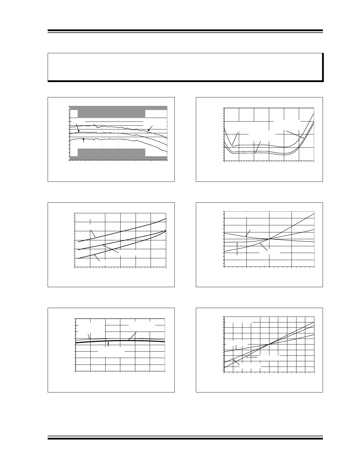
FIGURE 2-1:
Accuracy vs. Temperature
(TC72-X.XMXX).
FIGURE 2-2:
Supply Current vs. Supply
Voltage.
FIGURE 2-3:
Supply Current vs.
Temperature.
FIGURE 2-4:
Shutdown Current vs.
Temperature.
FIGURE 2-5:
Temperature Accuracy vs.
Supply Voltage (TC72-2.8MXX).
FIGURE 2-6:
Temperature Accuracy vs.
Supply Voltage (TC72-5.0MXX).
Note:
The graphs and tables provided following this note are a statistical summary based on a limited number of
samples and are provided for informational purposes only. The performance characteristics listed herein
are not tested or guaranteed. In some graphs or tables, the data presented may be outside the specified
operating range (e.g., outside specified power supply range) and therefore outside the warranted range.
-3.5
-3
-2.5
-2
-1.5
-1
-0.5
0
0.5
1
1.5
2
2.5
3
3.5
-55
-25
5
35
65
95
125
Reference Temperature (°C)
Temperature Error (°C)
Lower Specification Limit
Upper Specification Limit
Mean + 3V
Mean - 3V
Mean
200
210
220
230
240
250
260
2.5
3.0
3.5
4.0
4.5
5.0
5.5
Supply
Current (µA)
Supply Voltage (V)
T
A
= +25°C
T
A
= +125°C
T
A
= -55°C
TC72-X.XMXX
0
50
100
150
200
250
300
350
400
-55
-25
5
35
65
95
125
Supply
Current (uA)
Temperature (°C)
TC72-5.0MXX
V
DD
= 5.0V
TC72-3.3MXX
V
DD
= 3.3V
TC72-2.8MXX
V
DD
= 2.8V
0.00
0.05
0.10
0.15
0.20
-55
-25
5
35
65
95
125
Shutdow
n Current
(µA)
Temperature (°C)
TC72-5.0MXX
V
DD
= 5.0V
TC72-5.0MXX
V
DD
= 2.8V
TC72-3.3MXX
V
DD
= 3.3V
-0.4
-0.3
-0.2
-0.1
0.0
0.1
0.2
0.3
0.4
2.6
2.7
2.8
2.9
3.0
T
e
mperature Change
(°C)
Supply Voltage (V)
T
A
= +25°C
T
A
= -25°C
T
A
= +85°C
TC72-2.8MXX
-1.0
-0.8
-0.6
-0.4
-0.2
0.0
0.2
0.4
0.6
0.8
1.0
4.5 4.6 4.7 4.8 4.9 5.0 5.1 5.2 5.3 5.4 5.5
T
e
mperature Change
(°C)
Supply Voltage (V)
T
A
= +25°C
T
A
= -25°C
T
A
= +85°C
TC72-5.0MXX
TC72
DS21743B-page 8
© 2011 Microchip Technology Inc.
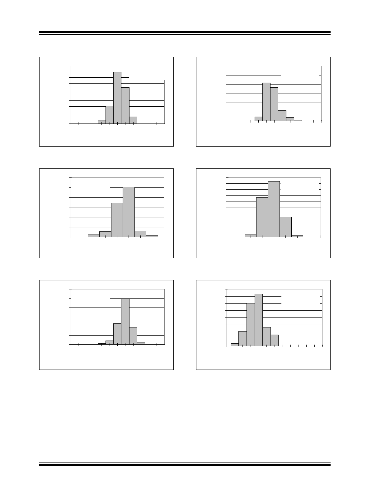
Note: Unless otherwise indicated, all parameters apply at V
DD
= 2.65V to 5.5V, T
A
= -55°C to +125°C.
FIGURE 2-7:
Histogram of Temperature
Accuracy at -55 Degrees C.
FIGURE 2-8:
Histogram of Temperature
Accuracy at -40 Degrees C.
FIGURE 2-9:
Histogram of Temperature
Accuracy at +25 Degrees C.
FIGURE 2-10:
Histogram of Temperature
Accuracy at +65 Degrees C.
FIGURE 2-11:
Histogram of Temperature
Accuracy at +85 Degrees C.
FIGURE 2-12:
Histogram of Temperature
Accuracy at +125 Degrees C.
0
5
10
15
20
25
30
35
40
45
50
-3
-2.5
-2
-1.5
-1
-0.5
0
0.5
1
1.5
2
2.5
3
Percentage of Occurances (%
)
Temperature Error (°C)
TC72-X.XMXX
Sample Size = 166
T
A
= -55°C
0
10
20
30
40
50
60
-2
-1.5
-1
-0.5
0
0.5
1
1.5
2
Percentage of Occurances (%
)
Temperature Error (°C)
TC72-X.XMXX
Sample Size = 166
T
A
= -40°C
0
10
20
30
40
50
60
-1.50
-1.25
-1.00
-0.75
-0.50
-0.25
0.00
0.25
0.50
0.75
1.00
1.25
1.50
Percentage of Occurances (%
)
Temperature Error (°C)
TC72-X.XMXX
Sample Size = 166
T
A
= +25°C
0
10
20
30
40
50
60
-1.50
-1.25
-1.00
-0.75
-0.50
-0.25
0.00
0.25
0.50
0.75
1.00
1.25
1.50
Percentage of Occurances (%
)
Temperature Error (°C)
TC72-X.XMXX
Sample Size = 166
T
A
= +65°C
0
5
10
15
20
25
30
35
40
45
50
-2
-1.5
-1
-0.5
0
0.5
1
1.5
2
Percentage of Occurances (%
)
Temperature Error (°C)
TC72-X.XMXX
Sample Size = 166
T
A
= +85°C
0
5
10
15
20
25
30
35
40
-3
-2.5
-2
-1.5
-1
-0.5
0
0.5
1
1.5
2
2.5
3
Percentage of Occurances (%
)
Temperature Error (°C)
TC72-X.XMXX
Sample Size = 166
T
A
= +125°C
© 2011 Microchip Technology Inc.
DS21743B-page 9
TC72
3.0
PIN DESCRIPTION
Pin functionalities are described in
Table 3-1
.
3.1
No Connection (NC)
This pin is not internally connected to the die.
3.2
Serial Clock Input (SCK)
The SCK pin is an Input pin. All communication and
timing is relative to the signal on this pin. The clock is
generated by the host controller on the SPI bus (see
Section 4.3 “Serial Bus Interface”
).
3.3
Chip Enable Input (CE)
The CE is a Chip Enable pin. This is an active high
input, therefore the device is enabled when CE is
toggled to V
DD
. Once the device is enabled, all serial
communication begins (see
Section 4.3 “Serial Bus
Interface”
).
3.4
Ground (GND)
The GND is the system Ground pin.
3.5
Serial Data Input (SDI)
The SDI is a Data Input pin, used to transmit data from
the host to the device (see
Section 4.3 “Serial Bus
Interface”
).
3.6
Serial Data Output (SDO)
The SDO is a Data Output pin, used to transmit data
from the device to the host (see
Section 4.3 “Serial
Bus Interface”
).
3.7
Power Supply (V
DD
)
V
DD
is the Power pin. The operating voltage range, as
specified in the DC electrical specification table, is
applied on this pin.
3.8
Exposed Pad (EP)
There is an internal electrical connection between the
Exposed Thermal Pad (EP) and the GND pin; they can
be connected to the same potential on the Printed
Circuit Board (PCB). This provides better thermal
conduction from the PCB to the die.
TABLE 3-1:
PIN FUNCTION TABLE
TC72
Symbol
Function
3x3 DFN
MSOP
1
1
NC
No internal connection
2
3
SCK
Serial Clock input
3
2
CE
Chip Enable input, the device is selected when this input is high
4
4
GND
Ground
5
6
SDI
Serial Data input
6
5
SDO
Serial Data output
7
7
NC
No internal connection
8
8
V
DD
Power supply
9
—
EP
Exposed pad (Ground)

TC72
DS21743B-page 10
© 2011 Microchip Technology Inc.
NOTES: