
2017 Microchip Technology Inc.
DS20005910A-page 1
MIC2810
Features
• 2.7V to 5.5V Input Voltage Range
• 2 MHz DC/DC Converter and Two LDOs
• Integrated Power-on Reset (POR)
• Adjustable POR Delay Time
• LOWQ Mode
- 30 µA Total I
Q
When in LOWQ Mode
• DC/DC Converter
- Up to 600 mA of Output Current in PWM
Mode
- LOWQ
Mode: No Ripple Light Load Mode
- 53 µV
RMS
Output Noise in LOWQ Mode
- 2 MHz PWM Mode Operation
- >90% Efficiency
• LDO1
- 1.65V to 5.5V Input Voltage Range
- 300 mA Output Current
- Output Voltage Down to 0.8V
• LDO2
- 2.7V to 5.5V Input Voltage Range
- 300 mA Output Current
- Output Voltage Down to 0.8V
• Thermal Shutdown Protection
• Current-Limit Protection
• Simple, Leakage-Free Interfacing to Host MPU in
Applications with Backup Power
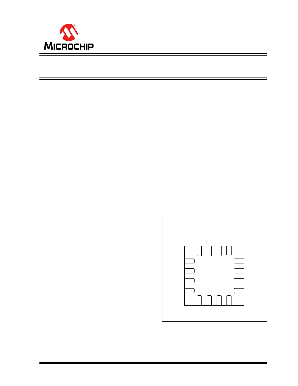
• Tiny 16-Pin 3 mm x 3 mm QFN Package
Applications
• Embedded MPU and MCU Power
• Portable and Wearable Applications
• Low-Power RF Systems
• Backup Power Systems
General Description
The MIC2810 is a high performance power
management IC, featuring three output voltages with
independent enable control: a 2 MHz DC/DC converter
and two 300 mA LDOs. The MIC2810 features a
LOWQ mode, reducing the total current draw while in
this mode to less than 30 µA. In LOWQ mode, the
output noise of the DC/DC converter is 53 µV
RMS
,
significantly lower than other converters that use a
PFM light load mode that can interfere with sensitive
RF circuitry.
The DC/DC converter uses small values of L and C to
reduce board space but still retains high efficiency over
a wide load range, while supporting load currents up to
600 mA.
The LDOs operate with very small ceramic output
capacitors for stability, therefore, reducing required
board space and component cost. It is available in
various output voltage options in the 16-pin 3 mm x
3 mm QFN leadless package.
Package Type
MIC2810
16-P
IN
3 mm
X
3 mm QFN
LOWQ
BIAS
SGND
PGND
POR
LDO1
VIN1
LDO
EN2
EN
EN1
CSET
SW
VIN
VIN2
LDO2
Pin 12
Pin 11
Pin 10
Pin 9
Pin 1
Pin 2
Pin 3
Pin 4
Pin 5
Pin 6
Pin 7
Pin 8
Pin 16
Pin 15
Pin 14
Pin 13
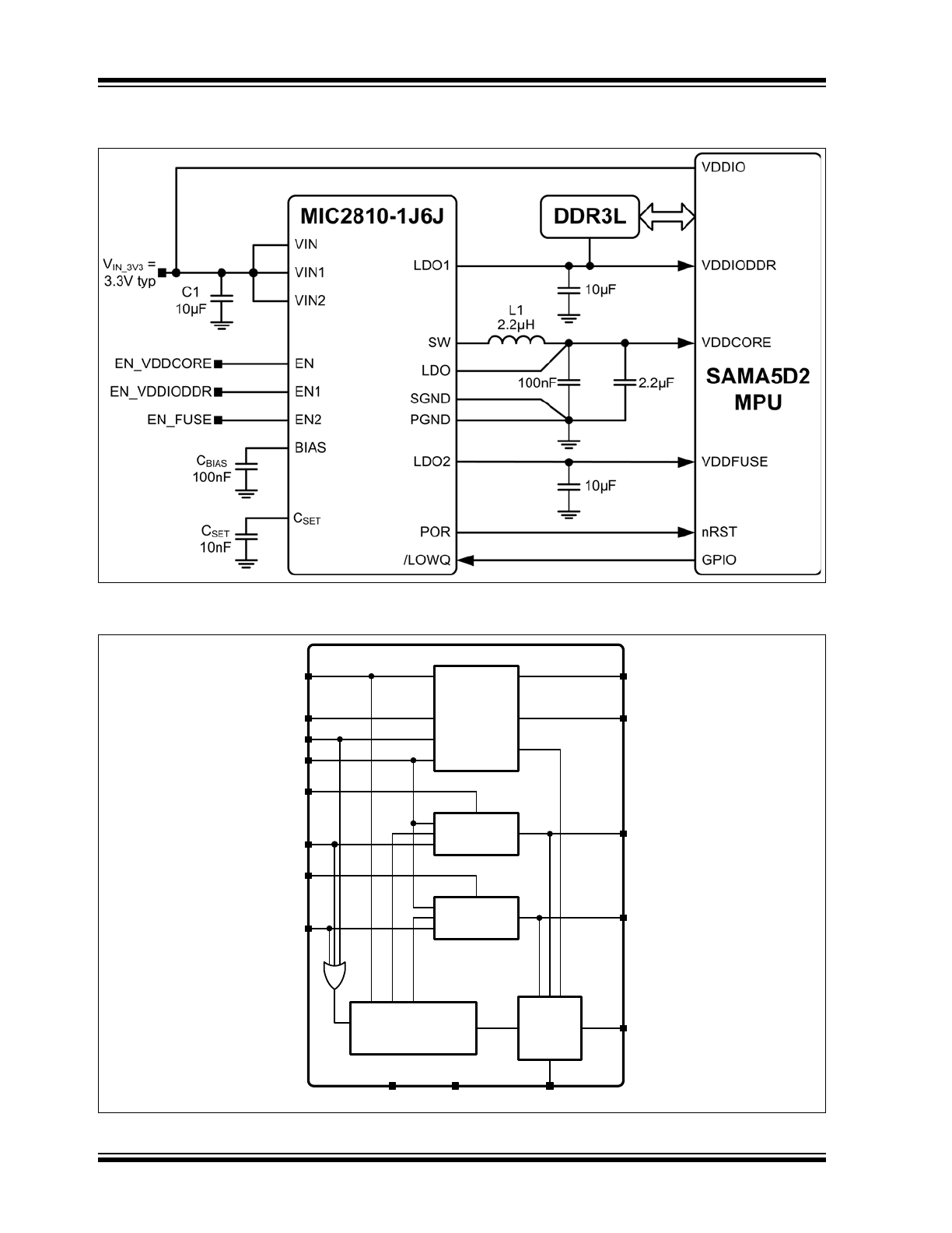
Digital Power Management IC 2 MHz, 600 mA DC/DC with Dual
300 mA/300 mA Low V
IN
LDOs
MIC2810
DS20005910A-page 2
2017 Microchip Technology Inc.
Typical Application Circuit (simplified)
Functional Diagram
VIN
LDO
DC/DC
VIN2
SW
LDO1
BIAS
EN
/LOWQ
LDO2
EN2
LDO1
LDO2
POR
LOGIC
POR
REFERENCE AND
QUICK START
SGND
PGND
C
SET
VIN1
EN1

2017 Microchip Technology Inc.
DS20005910A-page 3
MIC2810
1.0
ELECTRICAL CHARACTERISTICS
Absolute Maximum Ratings †
Supply Voltage (V
IN
, V
IN1
, V
IN2
)..................................................................................................................... 0V to +6.0V
Enable Input Voltage (V
EN
, V
EN1,
V
EN2
)..............................................................................................................0V to V
IN
Power Dissipation (
Note 1
) .................................................................................................................... Internally Limited
ESD Rating (
Note 2
) .................................................................................................................................................. 2 kV
Operating Ratings ‡
Supply Voltage (V
IN
, V
IN2
)......................................................................................................................... +2.7V to +5.5V
Supply Voltage (V
IN1
).............................................................................................................................. +1.65V to +5.5V
Enable Input Voltage (V
EN
, V
EN1,
V
EN2
)........................................................................................................... 0V to +V
IN
†
Notice: Stresses above those listed under “Absolute Maximum Ratings” may cause permanent damage to the device.
This is a stress rating only and functional operation of the device at those or any other conditions above those indicated
in the operational sections of this specification is not intended. Exposure to maximum rating conditions for extended
periods may affect device reliability.
‡ Notice:
The device is not guaranteed to function outside its operating ratings.
1:
The maximum allowable power dissipation of any T
A
(ambient temperature) is P
D(max)
= (T
J(max)
– T
A
) / θ
JA
.
Exceeding the maximum allowable power dissipation will result in excessive die temperature, and the
regulator will go into thermal shutdown.
2:
Devices are ESD sensitive. Handling precautions recommended. Human body model, 1.5 kΩ in series with
100 pF.
MIC2810
DS20005910A-page 4
2017 Microchip Technology Inc.
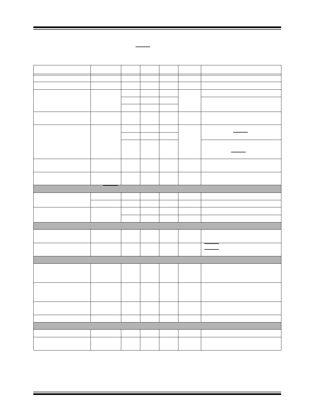
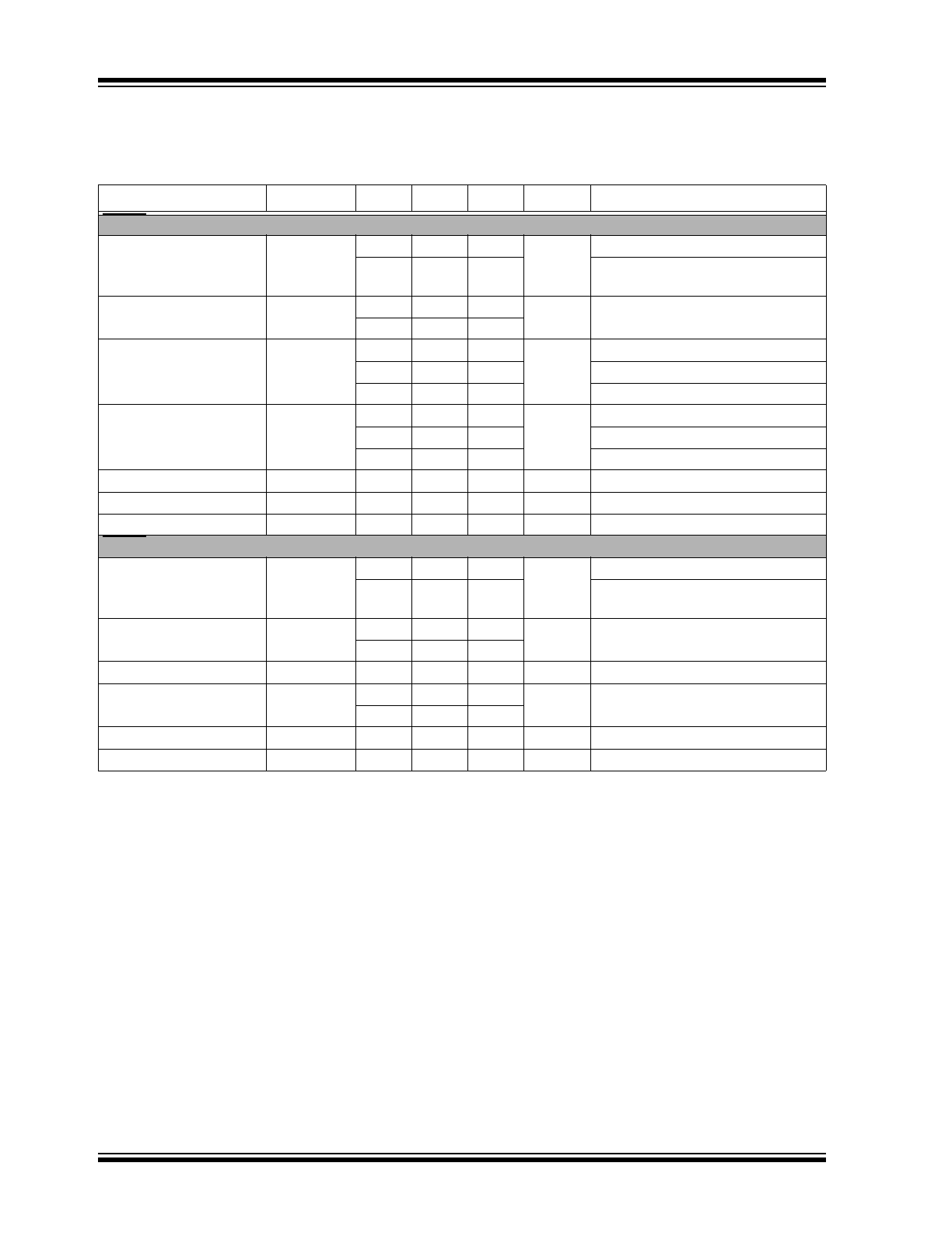
TABLE 1-1:
ELECTRICAL CHARACTERISTICS (
Note 1
)
Electrical Characteristics:
V
IN
= EN1 = EN2 = LOWQ = V
OUT
(
Note 2
) + 1V; C
OUTDC/DC
= 2.2 µF, C
LDO1
= C
LDO2
=
2.2 µF; I
OUTDC/DC
= 100 mA; I
OUTLDO1
= I
OUTLDO2
= 100 µA; T
J
= 25°C, bold values indicate –40°C ≤ T
J
≤ +125°C;
unless noted.
Parameter
Symbol
Min.
Typ.
Max.
Units
Conditions
UVLO Threshold
UVLO
TH
2.45
2.55
2.65
V
Rising input voltage during turn-on
UVLO Hysteresis
UVLO
HYS
—
100
—
mV
—
Ground Pin Current
I
GND
—
800
1100
µA
V
FB
= GND (not switching)
—
55
85
LDO1 or LDO2 (EN = GND; EN1 or
EN2 = GND)
—
—
95
Ground Pin Current in
Shutdown
I
GND_SHDN
—
0.2
5
µA
EN = EN1 = EN2 = 0V
Ground Pin Current
(LOWQ mode)
I
GND_LOWQ
—
30
60
µA
All channels on, I
DC/DC
= I
LDO1
=
I
LDO2
= 0 mA (LOWQ = GND)
—
—
80
—
20
70
LDO1 or LDO2 (EN = GND; EN1 or
EN2 = GND);
I
OUT
= 0 mA (LOWQ = GND)
Overtemperature
Shutdown
T
SD
—
160
—
°C
—
Overtemperature
Shutdown Hysteresis
T
SDHYS
—
23
—
°C
—
Enable Inputs (EN; EN1; EN2; LOWQ)
Enable Input Voltage
V
IH
—
—
0.2
V
Logic Low
V
IL
1.0
—
—
V
Logic High
Enable Input Current
I
ENLK
—
0.1
1
µA
V
IL
≤ 0.2V
—
0.1
1
µA
V
IH
≥ 1.0V
Turn-on Time
Turn-on Time
(LDO1 and LDO2)
t
TURN-ON
—
240
500
µs
—
Turn-on Time (DC/DC)
t
TURN-ON
—
83
350
µs
(LOWQ = V
IN
; I
LOAD
= 300 mA);
(LOWQ = GND; I
LOAD
= 10 mA)
POR Output
POR Threshold Voltage,
Falling
V
THLOW_POR
90
91
—
%
Low Threshold, % of nominal
(V
DC/DC
or V
LDO1
or V
LDO2
) (Flag
ON)
POR Threshold Voltage,
Rising
V
THIGH_POR
—
96
99
%
High Threshold, % of nominal
(V
DC/DC
and V
LDO1
and V
LDO2
)
(Flag OFF)
VOL
VOL
POR
—
10
100
mV
POR Output Logic Low Voltage; I
L
=
250 µA
IPOR ILEAK
POR
—
0.01
1
µA
Flag Leakage Current, Flag OFF
SET INPUT
SET Pin Current Source
I
SET
0.75
1.25
1.75
µA
V
SET
= 0V
SET Pin Threshold
Voltage
VTH
SET
—
1.25
—
V
POR = High
Note 1:
Specification for packaged product only.
2:
V
OUT
denotes the highest of the three output voltages of DC/DC, LDO1 and LDO2.
2017 Microchip Technology Inc.
DS20005910A-page 5
MIC2810
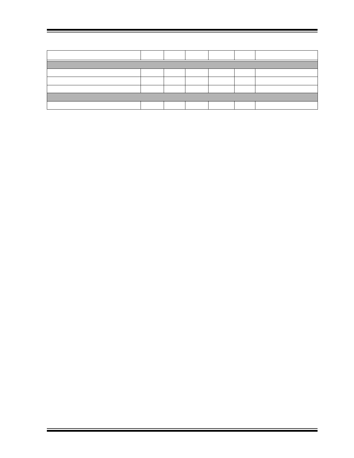
TABLE 1-2:
ELECTRICAL CHARACTERISTICS - DC/DC CONVERTER
Electrical Characteristics:
V
IN
= V
OUTDC/DC
+ 1V; EN1 = V
IN
; EN2 = GND; I
OUTDC/DC
= 100 mA; L = 2.2 µH;
C
OUTDC/DC
= 2.2 µF; T
J
= 25°C, bold values indicate –40°C to + 125°C; unless noted.
Parameter
Symbol
Min.
Typ.
Max.
Units
Conditions
LOWQ = High (Full Power Mode)
Output Voltage Accuracy
V
OUT
–2
—
2
%
Nominal V
OUT
tolerance
–3
—
3
Output Voltage Line
Regulation
(∆V
OUT
/V
OUT
)
/∆V
IN
—
0.2
—
%/V
V
OUT
> 2.4V; V
IN
= V
OUT
+ 300 mV
to 5.5V, I
LOAD
= 100 mA
V
OUT
< 2.4V; V
IN
= 2.7V to 5.5V,
I
LOAD
= 100 mA
Output Voltage Load
Regulation
∆V
OUT
/V
OUT
—
0.1
—
%
20 mA < I
LOAD
< 600 mA
Maximum Duty Cycle
DC
MAX
100
—
—
%
V
FB
≤ 0.4V
PWM Switch
ON-Resistance
—
—
0.5
—
Ω
I
SW
= 150 mA, V
FB
= 0.7V
FB_NOM
PMOS
—
0.6
—
Ω
I
SW
= –150 mA, V
FB
= 1.1V
FB_NOM
NMOS
Oscillator Frequency
f
osc
1.8
2
2.2
MHz
—
Current Limit in PWM
Mode
—
0.75
1
1.6
A
V
FB
= 0.9 * V
NOM
LOWQ = Low (Light Load Mode)
Output Voltage Accuracy
V
OUT
–2
—
2
%
Variation from nominal V
OUT
–3
—
3
Variation from nominal V
OUT
;
–40°C to +125°C
Line Regulation
(∆V
OUT
/V
OUT
)
/∆V
IN
—
0.02
0.3
%/V
V
IN
= V
OUT
+ 1V to 5.5V;
I
OUT
= 100 µA
—
—
0.6
Load Regulation
∆V
OUT
/V
OUT
—
0.4
1.5
%
I
OUT
= 100 µA to 50 mA
Ripple Rejection
PSRR
—
45
—
dB
f = up to 1 kHz
Current Limit
I
LIM_LOWQ
80
120
190
mA
V
OUT
= 0V
Output Voltage Noise
V
N
—
53
—
µV
RMS
10 Hz to 100 kHz
MIC2810
DS20005910A-page 6
2017 Microchip Technology Inc.
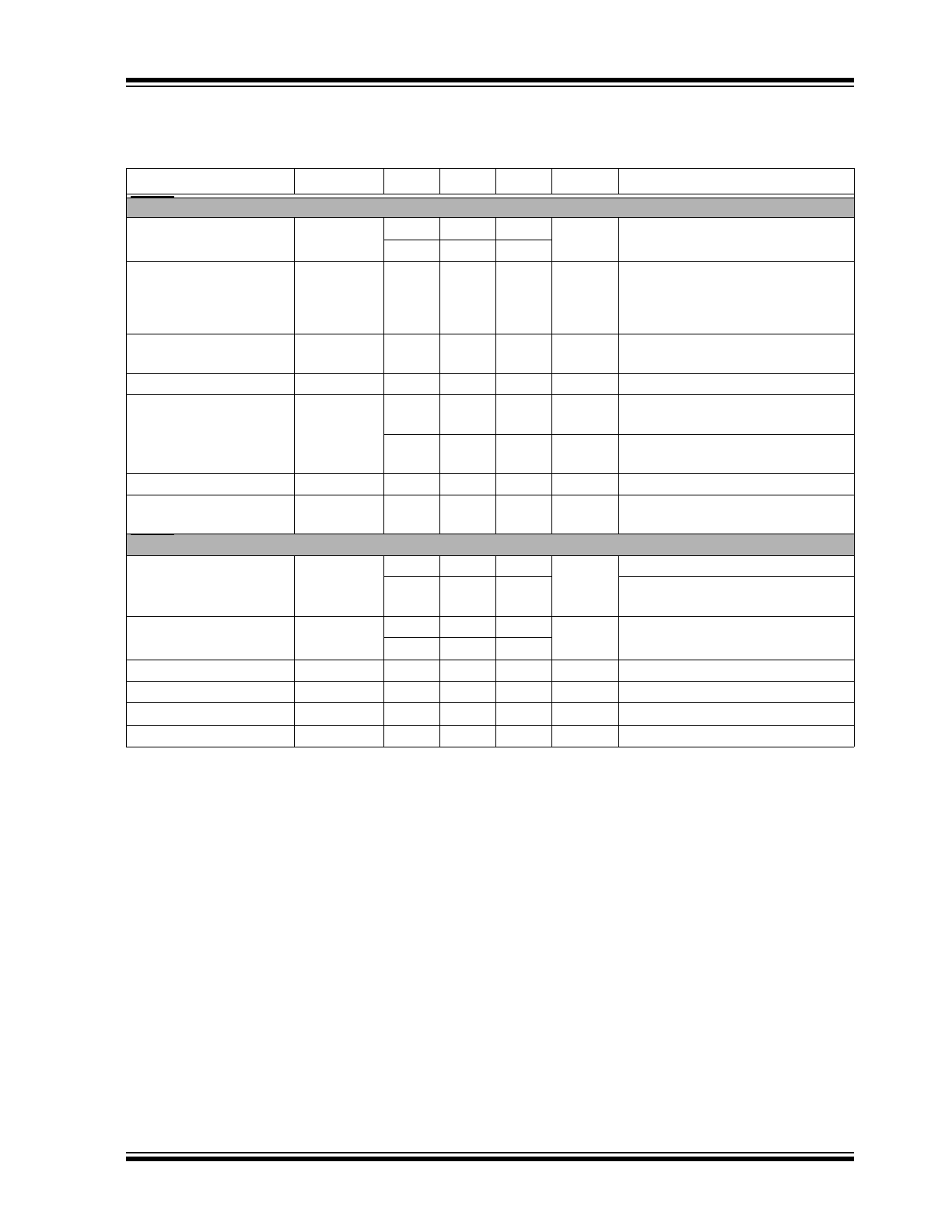
TABLE 1-3:
ELECTRICAL CHARACTERISTICS - LDO1/LDO2
Electrical Characteristics:
V
IN1
= V
IN2
= V
OUTLDO1
+ 1.0V or V
IN1
= V
IN2
= V
OUTLDO2
+ 1.0V; EN = GND; EN1 =
EN2 = V
IN1
= V
IN2
; C
LDO1
= C
LDO2
= 2.2 µF; I
OUTLDO1
= 100 µA; T
J
= 25°C, bold values indicate
–40°C ≤ T
J
≤ +125°C; unless noted.
Parameter
Symbol
Min.
Typ.
Max.
Units
Conditions
LOWQ = High (Full Power Mode)
Output Voltage Accuracy
V
OUT
–2
—
2
%
Variation from nominal V
OUT
–3
—
3
Variation from nominal V
OUT
;
–40°C to +125°C
Line Regulation
—
—
0.02
0.3
%/V
V
IN
= V
OUT
+1V to 5.5V
—
—
0.6
Load Regulation
∆V
OUT
/V
OUT
—
0.20
—
%
I
OUT
= 100 µA to 150 mA
—
0.25
—
I
OUT
= 100 µA to 200 mA
—
0.40
1.5
I
OUT
= 100 µA to 300 mA
Dropout Voltage
V
DO
—
70
—
mV
I
OUT
= 150 mA
—
94
—
I
OUT
= 200 mA
—
142
300
I
OUT
= 300 mA
Ripple Rejection
PSRR
—
35
—
dB
f = up to 1 kHz
Current Limit
I
LIM
400
600
850
mA
V
OUT
= 0V
Output Voltage Noise
V
N
—
91
—
µV
RMS
10 Hz to 100 kHz
LOWQ = Low (Light Load Mode)
Output Voltage Accuracy
V
OUT
–3
—
3
%
Variation from nominal V
OUT
–4
—
4
Variation from nominal V
OUT
;
–40°C to +125°C
Line Regulation
—
—
0.02
0.3
%/V
V
IN
= V
OUT
+1V to 5.5V
—
—
0.6
Load Regulation
∆V
OUT
/V
OUT
—
0.2
1.0
%
I
OUT
= 100 µA to 10 mA
Dropout Voltage
V
DO
—
22
35
mV
I
OUT
= 10 mA
—
—
50
Current Limit
I
LIM
50
85
125
mA
V
IN
= 2.7V; V
OUT
= 0V
Ripple Rejection
PSRR
—
35
—
dB
f = up to 1 kHz
2017 Microchip Technology Inc.
DS20005910A-page 7
MIC2810
TABLE 1-4:
TEMPERATURE SPECIFICATIONS (
Note 1
)
Parameters
Sym.
Min.
Typ.
Max.
Units
Conditions
Temperature Ranges
Storage Temperature Range
T
S
–65
—
+150
°C
—
Lead Temperature
—
—
—
+260
°C
Soldering, 10 sec.
Junction Temperature
T
J
–40
—
+125
°C
—
Package Thermal Resistance
16-Ld QFN
θ
JA
—
56
—
°C/W
—
Note 1:
The maximum allowable power dissipation is a function of ambient temperature, the maximum allowable
junction temperature and the thermal resistance from junction to air (i.e., T
A
, T
J
,
JA
). Exceeding the
maximum allowable power dissipation will cause the device operating junction temperature to exceed the
maximum +125°C rating. Sustained junction temperatures above +125°C can impact the device reliability.
MIC2810
DS20005910A-page 8
2017 Microchip Technology Inc.
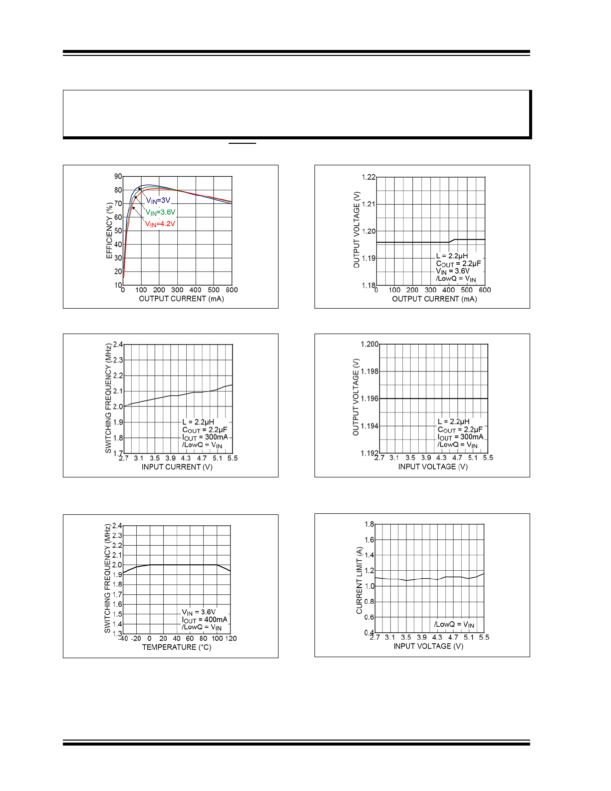
2.0
TYPICAL PERFORMANCE CURVES
For this page only, DC/DC Normal Mode (LOWQ = V
IN
)
FIGURE 2-1:
1.2V
OUT
Efficiency.
FIGURE 2-2:
Switching Frequency vs.
Input Voltage.
FIGURE 2-3:
Switching Frequency vs.
Temperature.
FIGURE 2-4:
Load Regulation.
FIGURE 2-5:
Line Regulation.
FIGURE 2-6:
Current Limit vs. Input
Voltage.
Note:
The graphs and tables provided following this note are a statistical summary based on a limited number of
samples and are provided for informational purposes only. The performance characteristics listed herein
are not tested or guaranteed. In some graphs or tables, the data presented may be outside the specified
operating range (e.g., outside specified power supply range) and therefore outside the warranted range.
2017 Microchip Technology Inc.
DS20005910A-page 9
MIC2810
For this page only, DC/DC LOWQ Mode (LOWQ = GND)
FIGURE 2-7:
Power Supply Rejection
Ratio.
FIGURE 2-8:
Load Regulation.
FIGURE 2-9:
Line Regulation.
FIGURE 2-10:
Current Limit vs. Input
Voltage.
FIGURE 2-11:
Output Noise Spectral
Density.
MIC2810
DS20005910A-page 10
2017 Microchip Technology Inc.
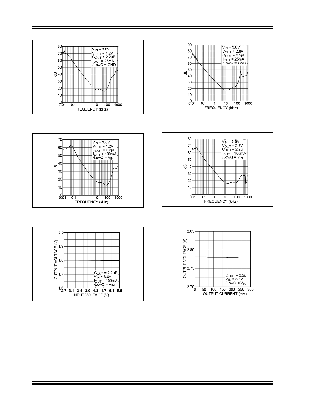
FIGURE 2-12:
Power Supply Rejection
Ratio LDO1 (LOWQ Mode).
FIGURE 2-13:
Power Supply Rejection
Ratio LDO1 (Normal Mode).
FIGURE 2-14:
LDO1 Line Regulation.
FIGURE 2-15:
Power Supply Rejection
Ratio LDO2 (LOWQ Mode).
FIGURE 2-16:
Power Supply Rejection
Ratio LDO2 (Normal Mode).
FIGURE 2-17:
LDO2 Load Regulation.