
R&E International
A Subsidiary of Microchip Technology Inc.
RE46C107
DC to DC Converter, Voltage Regulator and Piezoelectric Horn Driver
Product Specification
© 2009 Microchip Technology Inc. DS22160A-page 1
General Description
The RE46C107 is intended for use in 3V or 4.5V
battery or battery-backed applications. The circuit
features a DC-to-DC up-converter and driver circuit
suitable for driving a piezoelectric horn. A selectable
3.0V or 3.3V regulator is also provided for
microprocessor voltage regulation. An LED driver
and low battery detection and signaling are also
available.
Applications
Smoke detectors
CO Detectors
Personal Security Products
Electronic Toys
Features
• Low Quiescent Current
• 10V Up Converter
• Low Horn Driver Ron
• Voltage Regulation to 3.0V or 3.3V
• Low Battery Detection
•
Available in Standard Packaging or RoHS
Compliant Pb Free Packaging
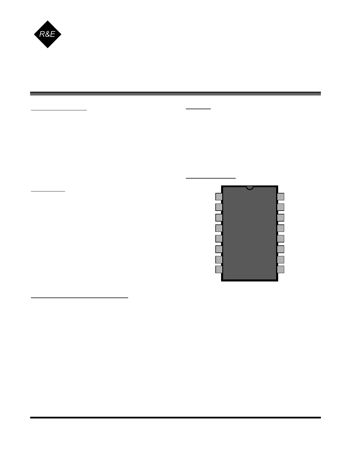
Pin Configuration
1
2
3
4
5
6
7
8
LBST
LBSET
VDD
LEDEN
LED
LX
VSS2
VSS
LBOUT
FEED
HRNEN
HORNS
HORNB
VO
VREG
REGSEL
16
15
14
13
12
11
10
9
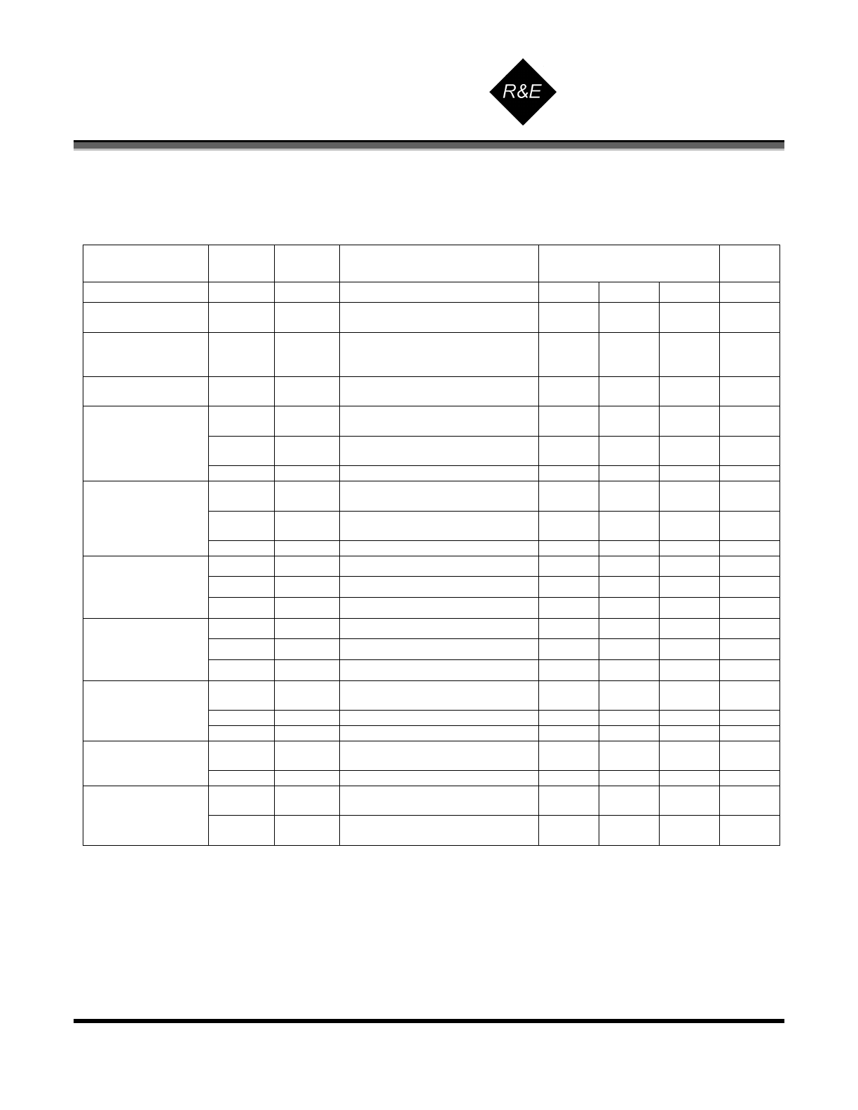
ABSOLUTE MAXIMUM RATINGS
PARAMETER
SYMBOL VALUE UNITS
Supply Voltage
V
DD
V
OUT
5
12
V
V
Input Voltage Range Except REGSEL & FEED
V
in
-.3 to V
reg
+.3 V
REGSEL Input Voltage Range
V
inrs
-.3 to V
dd
+.3 V
FEED Input Voltage Range
V
infd
-10 to +22
V
Input Current except FEED
I
in
10
mA
Operating Temperature
T
A
0 to 50
°C
Storage Temperature
T
STG
-55 to 125
°C
Continuous Operating Current
(HornS, HornB, Vreg, VO)
I
O
40
mA
Stresses beyond those listed under Absolute Maximum Ratings may cause permanent damage to the device. These are
stress ratings only and operation at these conditions for extended periods may affect device reliability.
This product utilizes CMOS technology with static protection; however proper ESD prevention procedures should be used
when handling this product. Damage can occur when exposed to extremely high static electrical charge

RE46C107
DC to DC Converter, Voltage Regulator and R&E International
Piezoelectric Horn Driver
A Subsidiary of Microchip Technology
Inc.
Product Specification
© 2009 Microchip Technology Inc. DS22160A-page 2
PIN DESCRIPTIONS
PIN#
PIN NAME
DESCRIPTION
1
LBST
Logic input used to activate low battery detection circuitry. This includes activating high
boost mode. Input is designed to interface with circuitry supplied by Vreg, so input voltage
levels will scale with the Vreg voltage. Input is disabled during brown-out.
2
LBSET
Internally connected to the low battery comparator input used to sense the Vdd voltage
divider. The internal reference to which this node is compared is nominally 0.9V. Nominal
internal resistance to Vdd is 400kohm. Nominal resistance to Vss is 240kohm. The
resistance to Vss is changed to a nominal of 220kohm once a low battery condition is
detected. External resistances can be added in parallel to adjust the low battery threshold
voltage.
3
VDD
Connect to the positive supply voltage
4
LEDEN
Logic input used to enable the LED driver. Input is designed to interface with circuitry
supplied by Vreg, so input voltage levels will scale with the Vreg voltage. LED driver is
disabled during brown-out.
5
LED
Open drain NMOS output used to drive a visible LED.
6
LX
Open drain NMOS output used to drive the boost converter inductor. The inductor should
be connected from this pin to the positive supply through a low resistance path.
7
VSS2
Internally connected to the source of the NMOS device used to drive the boost converter
inductor. Connect to the negative supply voltage through a low resistance path.
8
VSS
Connect to the negative supply voltage.
9
REGSEL
Logic input used to set the Vreg output voltage level. This input should always be tied to
either Vdd or Vss.
10
VREG
Regulated output voltage. Nominal output is 3.3V for REGSEL=Vdd and 3.0V for
REGSEL=Vss.
11
VO
Boosted voltage produced by DC-DC converter, typically 4V or 10V.
12
HORNB
This pin is connected to the metal electrode (B) of a piezoelectric transducer.
13
HORNS
HS is a complementary output to HB and connects to the ceramic electrode (S) of the
piezoelectric transducer.
14
HRNEN
Logic input for horn enable designed to interface with circuitry supplied by Vreg. Input
voltage levels will scale with the Vreg voltage. Horn is disabled during brown-out.
15
FEED
Usually connected to the feedback electrode of the piezoelectric horn through a current
limiting resistor. If not used, this pin must be connected to Vss.
16
LBOUT
Logic output used to signal a low battery condition. Output pulls to Vreg when LBST is
high and a low battery condition is detected.
RE46C107
DC to DC Converter, Voltage Regulator and R&E International
Piezoelectric Horn Driver
A Subsidiary of Microchip Technology
Inc.
Product Specification
© 2009 Microchip Technology Inc. DS22160A-page 3
Electrical Characteristics
Limits apply at Vdd=3V, Vss=Vss2=0V, Creg=10uF, Cvo=10uF, T
A
=0
°C to 50°C, unless otherwise noted.
Typical values are at T
A
=27
°C.
Limits
Parameter Symbol
Test
Pin Test
Conditions Min
Typ
Max
Units
Supply Voltage
Vdd
3
Operating
2.0 5.0 V
Standby Supply
Current
Iddstby
Inputs low; LBSET open; No
loads; DC-DC Running
14 uA
Quiescent Supply
Current
Iddq 3
Inputs low; LBSET open; No
loads;
VO=5V; Vlx=0.5V
7
10.5
uA
Quiescent Ivo
Ivoq
10
Same conditions as above for
Iddq
4
7.5
uA
Iil
1, 4, 14
LBST, LEDEN, HRNEN Inputs
Vin= VSS
-100
nA
Iilrs 9
REGSEL Input
Vin= Vss
-100
nA
Input Leakage Low
Iilf 15
FEED=-10V;
VO=10V
-15
-50
uA
Iih
1, 4, 14
LBST, LEDEN, HRNEN Inputs
Vin=Vreg
100
nA
Iihrs 9
REGSEL Input
Vin=Vdd
100
nA
Input Leakage High
Iihf 15
FEED=+22V;
VO=10V
20 50 uA
Vil
1, 4, 14
LBST, LEDEN, HRNEN Inputs
1
V
Vilrs 9
REGSEL
Input
1 V
Input Voltage Low
Vilf
15
FEED Input; VO=10V
3
V
Vih
1, 4, 14
LBST, LEDEN, HRNEN Inputs
Vreg-.7
V
Vihrs 9
REGSEL
Input
2.3
V
Input Voltage High
Vihf
15
FEED Input; VO=10V
7
V
Vol1 12,13
HORNB or HORNS; Iout=16mA;
Vdd=3V; VO=10V
.3 .5 V
Vol2
5
LED; Iout=10mA; VO=4V
.3
.5
V
Output Low
Voltage
Vol3
16
LBOUT; Iout=100uA; Vdd=3V
.3
.5
V
Voh1 12,13
HORNB or HORNS; VO=10V;
Iout=-16mA; HRNEN=Vreg
9.5 9.7
V
Output High
Voltage
Voh3
16
LBOUT; Iout=100uA; Vdd=2.1V
Vreg-.5
Vreg-.3
V
Vvo1 11
Vdd=3V; HRNEN=Vreg;
Iout=10mA
8.5 10 11 V
VO Output Voltage
Vvo2 11
Vdd=3V; HRNEN=0V;
Iout=10mA
3.5 4 4.4 V
RE46C107
DC to DC Converter, Voltage Regulator and R&E International
Piezoelectric Horn Driver
A Subsidiary of Microchip Technology
Inc.
Product Specification
© 2009 Microchip Technology Inc. DS22160A-page 4
Electrical Characteristics (continued)
Limits apply at Vdd=3V, Vss=Vss2=0V, Creg=10uF, Cvo=10uF, T
A
=0
°C to 50°C, unless otherwise noted.
Typical values are at T
A
=27
°C.
Limits
Parameter Symbol
Test
Pin Test
Conditions Min
Typ
Max
Units
Voeff1
Iload= 10mA, Vdd=3V;
HRNEN=0V
85 %
VO Efficiency
Voeff2
Iload=100uA; Vdd=3V;
HRNEN=0V
75 %
Low Battery
Threshold
Vlbat 3
LBST=Vreg
2.3 2.4
2.55 V
LBST to LBOUT
Propagation Delay
Tplhlb 16
Vdd=2.1;
LBSET Cload=5pF
10
20
us
Vreg1 10
Iout<20mA; REGSEL=Vdd
3.2 3.3 3.4 V
VREG Voltage
Vreg2 10
Iout<20mA; REGSEL=Vss
2.9 3.0 3.1 V
Vregld1 10
Iout=0 to 20mA; HRNEN=Vreg
30
50
mV
VREG Load
Regulation
Vregld2 10
Iout=0 to 20mA; HRNEN=0V
30
50
mV
Brownout
Threshold
Vobvt
11
Falling edge of VO 3.2
3.6
4.0
V
VO-to-Brownout
Margin
Vobvtm 11 Vv02
-Vobvt
100 400
mV
Brownout Pull
down
Ibt 10
VO=3.0V;
Vreg=2.0V
20 40 mA
Vcl1 10
REGSEL=Vdd
3.75 4 4.25 V
VREG over voltage
clamp
Vcl2 10
REGSEL=0V
3.35
3.6
3.85 V
Notes on Electrical Characteristics:
1/ DC-DC converter in high boost mode (nominal VO=10V) can draw current pulses of greater than 1 Amp and is therefore very sensitive to
series resistance. Critical components of this resistance are the inductor DC resistance, the internal resistance of the battery and the
resistance in the connections from the inductor to the battery, from the inductor to the LX pin and from the Vss2 pin to the battery. In order to
function properly under full load at Vdd=2V, the total of the inductor and interconnect resistances should not exceed 0.3 ohm. The internal
battery resistance should be no more than 0.5 ohm and a low ESR capacitor of 10uF or more should be connected in parallel with the battery
to average current draw over the boost converter cycle.
2/ In the Electrical Characteristics Table, wherever a specific VO value is listed under test conditions, the VO is forced externally with the
inductor disconnected and the DC-DC converter is NOT running.
3/ The brown-out threshold voltage is the VO voltage at which the regulator and horn will be disabled. At VO voltages below the brown-out
threshold Vreg will be pulled to Vss.
4/ In normal operation, the regulator will provide high-side current of up to 20mA, but current sinking capability is typically under 1uA. The
overvoltage clamp is intended to limit the voltage at Vreg when it is pulled up by an external source.
5/ The limits shown are 100% tested at 25C only. Test limits are guard-banded based on temperature characterization to guarantee
compliance at temperature extremes.
RE46C107
DC to DC Converter, Voltage Regulator and R&E International
Piezoelectric Horn Driver
A Subsidiary of Microchip Technology
Inc.
Product Specification
© 2009 Microchip Technology Inc. DS22160A-page 5
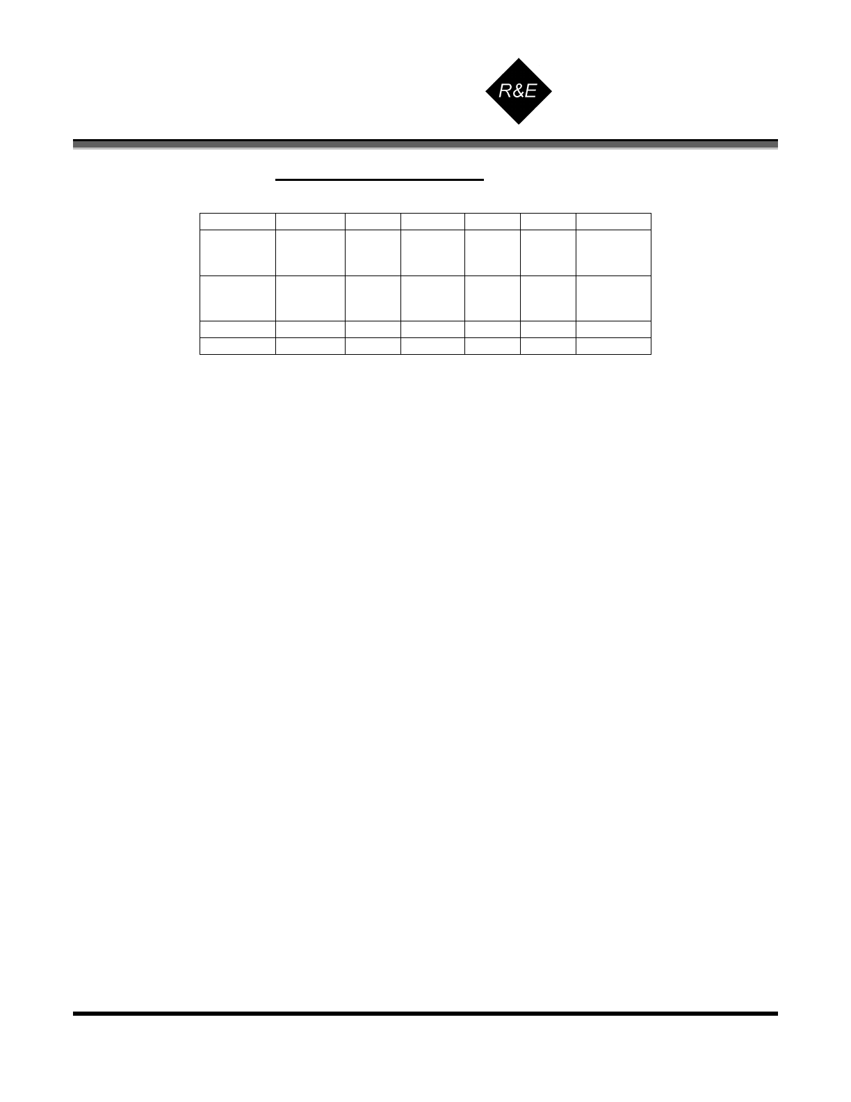
Truth Table - Horn/Boost Logic
Status
LBST HRNEN FEED HORNB
HORNS
VO
(Typ.)
Low Battery
Disabled;
Horn
Disabled
0 0 X 0
0
Vvo2
(4V)
Low Battery
Enabled;
Horn
Disabled
1 0 X 0
0
Vvo1
(10V)
Horn Enabled
X
1
0
1
0
Vvo1 (10V)
Horn Enabled
X
1
1
0
1
Vvo1 (10V)
RE46C107
DC to DC Converter, Voltage Regulator and R&E International
Piezoelectric Horn Driver
A Subsidiary of Microchip Technology
Inc.
Product Specification
© 2009 Microchip Technology Inc. DS22160A-page 6
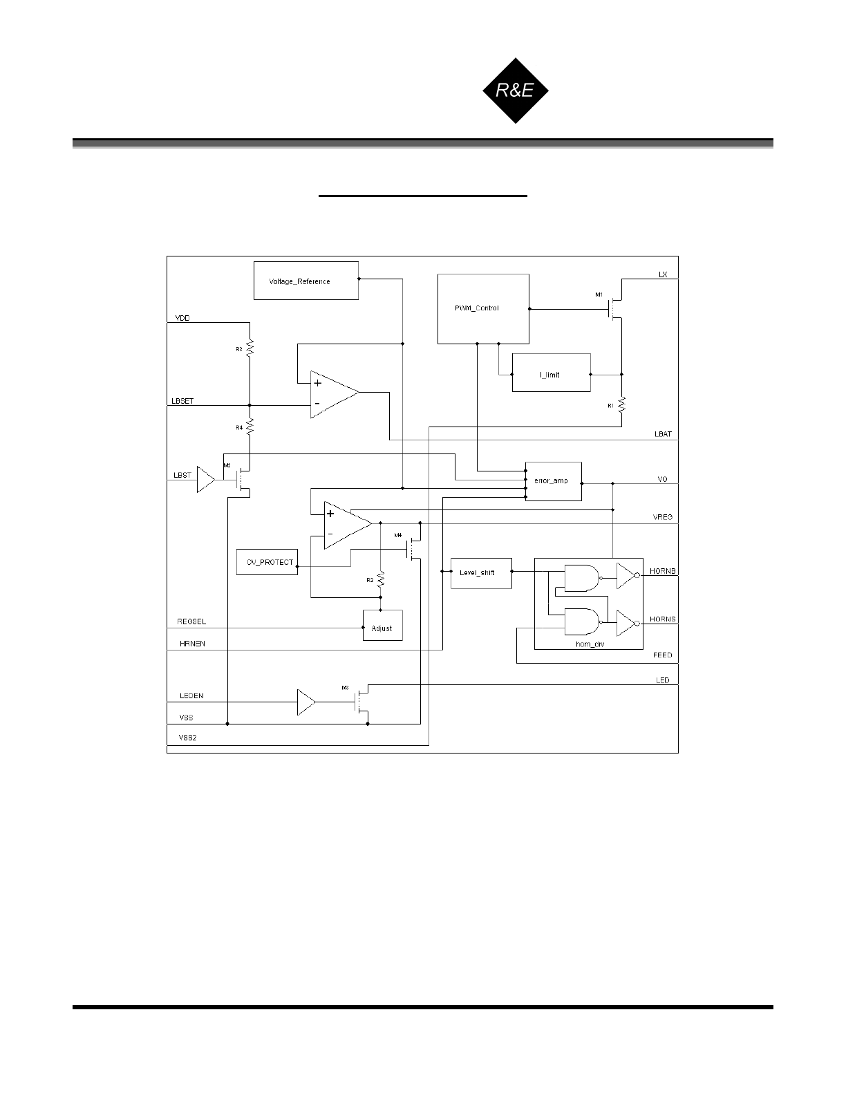
Functional Block Diagram
RE46C107
DC to DC Converter, Voltage Regulator and R&E International
Piezoelectric Horn Driver
A Subsidiary of Microchip Technology
Inc.
Product Specification
© 2009 Microchip Technology Inc. DS22160A-page 7
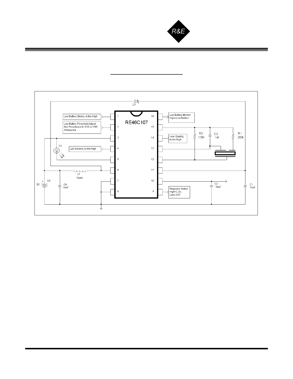
Typical Application Circuit
Notes:
1/ Schottky diode D1 must have maximum peak current rating of at least 1.5A and for best results should have forward voltage spec of less
than 0.5V at 1 Amp.
2/ Inductor L1 must have maximum peak current rating of at least 1.5A and for best results should have DC resistance of less than 0.3 ohm.
RE46C107
DC to DC Converter, Voltage Regulator and R&E International
Piezoelectric Horn Driver
A Subsidiary of Microchip Technology
Inc.
Product Specification
© 2009 Microchip Technology Inc. DS22160A-page 8
Information contained in this publication regarding device
applications and the like is provided only for your convenience and
may be superseded by updates. It is your responsibility to ensure
that your application meets with your specifications. MICROCHIP
MAKES NO REPRESENTATIONS OR WARRANTIES OF ANY
KIND WHETHER EXPRESS OR IMPLIED, WRITTEN OR ORAL,
STATUTORY OR OTHERWISE, RELATED TO THE
INFORMATION, INCLUDING BUT NOT LIMITED TO ITS
CONDITION, QUALITY, PERFORMANCE, MERCHANTABILITY
OR FITNESS FOR PURPOSE. Microchip disclaims all liability
arising from this information and its use. Use of Microchip devices in
life support and/or safety applications is entirely at the buyer’s risk,
and the buyer agrees to defend, indemnify and hold harmless
Microchip from any and all damages, claims, suits, or expenses
resulting from such use. No licenses are conveyed, implicitly or
otherwise, under any Microchip intellectual property rights.
Trademarks
The Microchip name and logo, the Microchip logo, Accuron,
dsPIC, K
EE
L
OQ
, K
EE
L
OQ
logo,
MPLAB, PIC, PICmicro,
PICSTART, rfPIC, SmartShunt and UNI/O are registered
trademarks of Microchip Technology Incorporated in the U.S.A.
and other countries.
FilterLab, Hampshire, Linear Active Thermistor, MXDEV, MXLAB,
SEEVAL, SmartSensor and The Embedded Control Solutions
Company are registered trademarks of Microchip Technology
Incorporated in the U.S.A.
Analog-for-the-Digital Age, Application Maestro, CodeGuard,
dsPICDEM, dsPICDEM.net, dsPICworks, dsSPEAK, ECAN,
ECONOMONITOR, FanSense, In-Circuit Serial Programming,
ICSP, ICEPIC, Mindi, MiWi, MPASM, MPLAB Certified logo,
MPLIB, MPLINK, mTouch, nanoWatt XLP, PICkit, PICDEM,
PICDEM.net, PICtail, PIC
32
logo, PowerCal, PowerInfo,
PowerMate, PowerTool, REAL ICE, rfLAB, Select Mode, Total
Endurance, TSHARC, WiperLock and ZENA are trademarks of
Microchip Technology Incorporated in the U.S.A. and other
countries.
SQTP is a service mark of Microchip Technology Incorporated in
the U.S.A.
All other trademarks mentioned herein are property of their
respective companies.
© 2009, Microchip Technology Incorporated, Printed in the
U.S.A., All Rights Reserved.
Printed on recycled paper.
Microchip received ISO/TS-16949:2002 certification for its worldwide
headquarters, design and wafer fabrication facilities in Chandler and
Tempe, Arizona; Gresham, Oregon and design centers in California and
India. The Company’s quality system processes and procedures are for its
PIC
®
MCUs and dsPIC
®
DSCs, K
EE
L
OQ
®
code hopping devices, Serial
EEPROMs, microperipherals, nonvolatile memory and analog products. In
addition, Microchip’s quality system for the design and manufacture of
development systems is ISO 9001:2000 certified.

RE46C107
DC to DC Converter, Voltage Regulator and R&E International
Piezoelectric Horn Driver
A Subsidiary of Microchip Technology
Inc.
Product Specification
© 2009 Microchip Technology Inc. DS22160A-page 9
R&E International
A Subsidiary of Microchip Technology Inc.
RE46C107
DC to DC Converter, Voltage Regulator and Piezoelectric Horn Driver
Product Specification
© 2009 Microchip Technology Inc. DS22160A-page 1
General Description
The RE46C107 is intended for use in 3V or 4.5V
battery or battery-backed applications. The circuit
features a DC-to-DC up-converter and driver circuit
suitable for driving a piezoelectric horn. A selectable
3.0V or 3.3V regulator is also provided for
microprocessor voltage regulation. An LED driver
and low battery detection and signaling are also
available.
Applications
Smoke detectors
CO Detectors
Personal Security Products
Electronic Toys
Features
• Low Quiescent Current
• 10V Up Converter
• Low Horn Driver Ron
• Voltage Regulation to 3.0V or 3.3V
• Low Battery Detection
•
Available in Standard Packaging or RoHS
Compliant Pb Free Packaging
Pin Configuration
1
2
3
4
5
6
7
8
LBST
LBSET
VDD
LEDEN
LED
LX
VSS2
VSS
LBOUT
FEED
HRNEN
HORNS
HORNB
VO
VREG
REGSEL
16
15
14
13
12
11
10
9
ABSOLUTE MAXIMUM RATINGS
PARAMETER
SYMBOL VALUE UNITS
Supply Voltage
V
DD
V
OUT
5
12
V
V
Input Voltage Range Except REGSEL & FEED
V
in
-.3 to V
reg
+.3 V
REGSEL Input Voltage Range
V
inrs
-.3 to V
dd
+.3 V
FEED Input Voltage Range
V
infd
-10 to +22
V
Input Current except FEED
I
in
10
mA
Operating Temperature
T
A
0 to 50
°C
Storage Temperature
T
STG
-55 to 125
°C
Continuous Operating Current
(HornS, HornB, Vreg, VO)
I
O
40
mA
Stresses beyond those listed under Absolute Maximum Ratings may cause permanent damage to the device. These are
stress ratings only and operation at these conditions for extended periods may affect device reliability.
This product utilizes CMOS technology with static protection; however proper ESD prevention procedures should be used
when handling this product. Damage can occur when exposed to extremely high static electrical charge
RE46C107
DC to DC Converter, Voltage Regulator and R&E International
Piezoelectric Horn Driver
A Subsidiary of Microchip Technology
Inc.
Product Specification
© 2009 Microchip Technology Inc. DS22160A-page 2
PIN DESCRIPTIONS
PIN#
PIN NAME
DESCRIPTION
1
LBST
Logic input used to activate low battery detection circuitry. This includes activating high
boost mode. Input is designed to interface with circuitry supplied by Vreg, so input voltage
levels will scale with the Vreg voltage. Input is disabled during brown-out.
2
LBSET
Internally connected to the low battery comparator input used to sense the Vdd voltage
divider. The internal reference to which this node is compared is nominally 0.9V. Nominal
internal resistance to Vdd is 400kohm. Nominal resistance to Vss is 240kohm. The
resistance to Vss is changed to a nominal of 220kohm once a low battery condition is
detected. External resistances can be added in parallel to adjust the low battery threshold
voltage.
3
VDD
Connect to the positive supply voltage
4
LEDEN
Logic input used to enable the LED driver. Input is designed to interface with circuitry
supplied by Vreg, so input voltage levels will scale with the Vreg voltage. LED driver is
disabled during brown-out.
5
LED
Open drain NMOS output used to drive a visible LED.
6
LX
Open drain NMOS output used to drive the boost converter inductor. The inductor should
be connected from this pin to the positive supply through a low resistance path.
7
VSS2
Internally connected to the source of the NMOS device used to drive the boost converter
inductor. Connect to the negative supply voltage through a low resistance path.
8
VSS
Connect to the negative supply voltage.
9
REGSEL
Logic input used to set the Vreg output voltage level. This input should always be tied to
either Vdd or Vss.
10
VREG
Regulated output voltage. Nominal output is 3.3V for REGSEL=Vdd and 3.0V for
REGSEL=Vss.
11
VO
Boosted voltage produced by DC-DC converter, typically 4V or 10V.
12
HORNB
This pin is connected to the metal electrode (B) of a piezoelectric transducer.
13
HORNS
HS is a complementary output to HB and connects to the ceramic electrode (S) of the
piezoelectric transducer.
14
HRNEN
Logic input for horn enable designed to interface with circuitry supplied by Vreg. Input
voltage levels will scale with the Vreg voltage. Horn is disabled during brown-out.
15
FEED
Usually connected to the feedback electrode of the piezoelectric horn through a current
limiting resistor. If not used, this pin must be connected to Vss.
16
LBOUT
Logic output used to signal a low battery condition. Output pulls to Vreg when LBST is
high and a low battery condition is detected.
RE46C107
DC to DC Converter, Voltage Regulator and R&E International
Piezoelectric Horn Driver
A Subsidiary of Microchip Technology
Inc.
Product Specification
© 2009 Microchip Technology Inc. DS22160A-page 3
Electrical Characteristics
Limits apply at Vdd=3V, Vss=Vss2=0V, Creg=10uF, Cvo=10uF, T
A
=0
°C to 50°C, unless otherwise noted.
Typical values are at T
A
=27
°C.
Limits
Parameter Symbol
Test
Pin Test
Conditions Min
Typ
Max
Units
Supply Voltage
Vdd
3
Operating
2.0 5.0 V
Standby Supply
Current
Iddstby
Inputs low; LBSET open; No
loads; DC-DC Running
14 uA
Quiescent Supply
Current
Iddq 3
Inputs low; LBSET open; No
loads;
VO=5V; Vlx=0.5V
7
10.5
uA
Quiescent Ivo
Ivoq
10
Same conditions as above for
Iddq
4
7.5
uA
Iil
1, 4, 14
LBST, LEDEN, HRNEN Inputs
Vin= VSS
-100
nA
Iilrs 9
REGSEL Input
Vin= Vss
-100
nA
Input Leakage Low
Iilf 15
FEED=-10V;
VO=10V
-15
-50
uA
Iih
1, 4, 14
LBST, LEDEN, HRNEN Inputs
Vin=Vreg
100
nA
Iihrs 9
REGSEL Input
Vin=Vdd
100
nA
Input Leakage High
Iihf 15
FEED=+22V;
VO=10V
20 50 uA
Vil
1, 4, 14
LBST, LEDEN, HRNEN Inputs
1
V
Vilrs 9
REGSEL
Input
1 V
Input Voltage Low
Vilf
15
FEED Input; VO=10V
3
V
Vih
1, 4, 14
LBST, LEDEN, HRNEN Inputs
Vreg-.7
V
Vihrs 9
REGSEL
Input
2.3
V
Input Voltage High
Vihf
15
FEED Input; VO=10V
7
V
Vol1 12,13
HORNB or HORNS; Iout=16mA;
Vdd=3V; VO=10V
.3 .5 V
Vol2
5
LED; Iout=10mA; VO=4V
.3
.5
V
Output Low
Voltage
Vol3
16
LBOUT; Iout=100uA; Vdd=3V
.3
.5
V
Voh1 12,13
HORNB or HORNS; VO=10V;
Iout=-16mA; HRNEN=Vreg
9.5 9.7
V
Output High
Voltage
Voh3
16
LBOUT; Iout=100uA; Vdd=2.1V
Vreg-.5
Vreg-.3
V
Vvo1 11
Vdd=3V; HRNEN=Vreg;
Iout=10mA
8.5 10 11 V
VO Output Voltage
Vvo2 11
Vdd=3V; HRNEN=0V;
Iout=10mA
3.5 4 4.4 V
RE46C107
DC to DC Converter, Voltage Regulator and R&E International
Piezoelectric Horn Driver
A Subsidiary of Microchip Technology
Inc.
Product Specification
© 2009 Microchip Technology Inc. DS22160A-page 4
Electrical Characteristics (continued)
Limits apply at Vdd=3V, Vss=Vss2=0V, Creg=10uF, Cvo=10uF, T
A
=0
°C to 50°C, unless otherwise noted.
Typical values are at T
A
=27
°C.
Limits
Parameter Symbol
Test
Pin Test
Conditions Min
Typ
Max
Units
Voeff1
Iload= 10mA, Vdd=3V;
HRNEN=0V
85 %
VO Efficiency
Voeff2
Iload=100uA; Vdd=3V;
HRNEN=0V
75 %
Low Battery
Threshold
Vlbat 3
LBST=Vreg
2.3 2.4
2.55 V
LBST to LBOUT
Propagation Delay
Tplhlb 16
Vdd=2.1;
LBSET Cload=5pF
10
20
us
Vreg1 10
Iout<20mA; REGSEL=Vdd
3.2 3.3 3.4 V
VREG Voltage
Vreg2 10
Iout<20mA; REGSEL=Vss
2.9 3.0 3.1 V
Vregld1 10
Iout=0 to 20mA; HRNEN=Vreg
30
50
mV
VREG Load
Regulation
Vregld2 10
Iout=0 to 20mA; HRNEN=0V
30
50
mV
Brownout
Threshold
Vobvt
11
Falling edge of VO 3.2
3.6
4.0
V
VO-to-Brownout
Margin
Vobvtm 11 Vv02
-Vobvt
100 400
mV
Brownout Pull
down
Ibt 10
VO=3.0V;
Vreg=2.0V
20 40 mA
Vcl1 10
REGSEL=Vdd
3.75 4 4.25 V
VREG over voltage
clamp
Vcl2 10
REGSEL=0V
3.35
3.6
3.85 V
Notes on Electrical Characteristics:
1/ DC-DC converter in high boost mode (nominal VO=10V) can draw current pulses of greater than 1 Amp and is therefore very sensitive to
series resistance. Critical components of this resistance are the inductor DC resistance, the internal resistance of the battery and the
resistance in the connections from the inductor to the battery, from the inductor to the LX pin and from the Vss2 pin to the battery. In order to
function properly under full load at Vdd=2V, the total of the inductor and interconnect resistances should not exceed 0.3 ohm. The internal
battery resistance should be no more than 0.5 ohm and a low ESR capacitor of 10uF or more should be connected in parallel with the battery
to average current draw over the boost converter cycle.
2/ In the Electrical Characteristics Table, wherever a specific VO value is listed under test conditions, the VO is forced externally with the
inductor disconnected and the DC-DC converter is NOT running.
3/ The brown-out threshold voltage is the VO voltage at which the regulator and horn will be disabled. At VO voltages below the brown-out
threshold Vreg will be pulled to Vss.
4/ In normal operation, the regulator will provide high-side current of up to 20mA, but current sinking capability is typically under 1uA. The
overvoltage clamp is intended to limit the voltage at Vreg when it is pulled up by an external source.
5/ The limits shown are 100% tested at 25C only. Test limits are guard-banded based on temperature characterization to guarantee
compliance at temperature extremes.
RE46C107
DC to DC Converter, Voltage Regulator and R&E International
Piezoelectric Horn Driver
A Subsidiary of Microchip Technology
Inc.
Product Specification
© 2009 Microchip Technology Inc. DS22160A-page 5
Truth Table - Horn/Boost Logic
Status
LBST HRNEN FEED HORNB
HORNS
VO
(Typ.)
Low Battery
Disabled;
Horn
Disabled
0 0 X 0
0
Vvo2
(4V)
Low Battery
Enabled;
Horn
Disabled
1 0 X 0
0
Vvo1
(10V)
Horn Enabled
X
1
0
1
0
Vvo1 (10V)
Horn Enabled
X
1
1
0
1
Vvo1 (10V)
RE46C107
DC to DC Converter, Voltage Regulator and R&E International
Piezoelectric Horn Driver
A Subsidiary of Microchip Technology
Inc.
Product Specification
© 2009 Microchip Technology Inc. DS22160A-page 6
Functional Block Diagram
RE46C107
DC to DC Converter, Voltage Regulator and R&E International
Piezoelectric Horn Driver
A Subsidiary of Microchip Technology
Inc.
Product Specification
© 2009 Microchip Technology Inc. DS22160A-page 7
Typical Application Circuit
Notes:
1/ Schottky diode D1 must have maximum peak current rating of at least 1.5A and for best results should have forward voltage spec of less
than 0.5V at 1 Amp.
2/ Inductor L1 must have maximum peak current rating of at least 1.5A and for best results should have DC resistance of less than 0.3 ohm.
RE46C107
DC to DC Converter, Voltage Regulator and R&E International
Piezoelectric Horn Driver
A Subsidiary of Microchip Technology
Inc.
Product Specification
© 2009 Microchip Technology Inc. DS22160A-page 8
Information contained in this publication regarding device
applications and the like is provided only for your convenience and
may be superseded by updates. It is your responsibility to ensure
that your application meets with your specifications. MICROCHIP
MAKES NO REPRESENTATIONS OR WARRANTIES OF ANY
KIND WHETHER EXPRESS OR IMPLIED, WRITTEN OR ORAL,
STATUTORY OR OTHERWISE, RELATED TO THE
INFORMATION, INCLUDING BUT NOT LIMITED TO ITS
CONDITION, QUALITY, PERFORMANCE, MERCHANTABILITY
OR FITNESS FOR PURPOSE. Microchip disclaims all liability
arising from this information and its use. Use of Microchip devices in
life support and/or safety applications is entirely at the buyer’s risk,
and the buyer agrees to defend, indemnify and hold harmless
Microchip from any and all damages, claims, suits, or expenses
resulting from such use. No licenses are conveyed, implicitly or
otherwise, under any Microchip intellectual property rights.
Trademarks
The Microchip name and logo, the Microchip logo, Accuron,
dsPIC, K
EE
L
OQ
, K
EE
L
OQ
logo,
MPLAB, PIC, PICmicro,
PICSTART, rfPIC, SmartShunt and UNI/O are registered
trademarks of Microchip Technology Incorporated in the U.S.A.
and other countries.
FilterLab, Hampshire, Linear Active Thermistor, MXDEV, MXLAB,
SEEVAL, SmartSensor and The Embedded Control Solutions
Company are registered trademarks of Microchip Technology
Incorporated in the U.S.A.
Analog-for-the-Digital Age, Application Maestro, CodeGuard,
dsPICDEM, dsPICDEM.net, dsPICworks, dsSPEAK, ECAN,
ECONOMONITOR, FanSense, In-Circuit Serial Programming,
ICSP, ICEPIC, Mindi, MiWi, MPASM, MPLAB Certified logo,
MPLIB, MPLINK, mTouch, nanoWatt XLP, PICkit, PICDEM,
PICDEM.net, PICtail, PIC
32
logo, PowerCal, PowerInfo,
PowerMate, PowerTool, REAL ICE, rfLAB, Select Mode, Total
Endurance, TSHARC, WiperLock and ZENA are trademarks of
Microchip Technology Incorporated in the U.S.A. and other
countries.
SQTP is a service mark of Microchip Technology Incorporated in
the U.S.A.
All other trademarks mentioned herein are property of their
respective companies.
© 2009, Microchip Technology Incorporated, Printed in the
U.S.A., All Rights Reserved.
Printed on recycled paper.
Microchip received ISO/TS-16949:2002 certification for its worldwide
headquarters, design and wafer fabrication facilities in Chandler and
Tempe, Arizona; Gresham, Oregon and design centers in California and
India. The Company’s quality system processes and procedures are for its
PIC
®
MCUs and dsPIC
®
DSCs, K
EE
L
OQ
®
code hopping devices, Serial
EEPROMs, microperipherals, nonvolatile memory and analog products. In
addition, Microchip’s quality system for the design and manufacture of
development systems is ISO 9001:2000 certified.
RE46C107
DC to DC Converter, Voltage Regulator and R&E International
Piezoelectric Horn Driver
A Subsidiary of Microchip Technology
Inc.
Product Specification
© 2009 Microchip Technology Inc. DS22160A-page 9