
Features
•
High Performance, Low Power 32-bit Atmel
®
AVR
®
Microcontroller
– Compact Single-Cycle RISC Instruction Set Including DSP Instruction Set
– Read-Modify-Write Instructions and Atomic Bit Manipulation
– Performing up to 1.51DMIPS/MHz
• Up to 126 DMIPS Running at 84MHz from Flash (1 Wait-State)
• Up to 63 DMIPS Running at 42MHz from Flash (0 Wait-State)
– Memory Protection Unit
•
Multi-Layer Bus System
– High-Performance Data Transfers on Separate Buses for Increased Performance
– 8 Peripheral DMA Channels (PDCA) Improves Speed for Peripheral
Communication
– 4 generic DMA Channels for High Bandwidth Data Paths
•
Internal High-Speed Flash
– 256KBytes, 128KBytes, 64KBytes versions
– Single-Cycle Flash Access up to 36MHz
– Prefetch Buffer Optimizing Instruction Execution at Maximum Speed
– 4 ms Page Programming Time and 8ms Full-Chip Erase Time
– 100,000 Write Cycles, 15-year Data Retention Capability
– Flash Security Locks and User Defined Configuration Area
•
Internal High-Speed SRAM
– 64KBytes Single-Cycle Access at Full Speed, Connected to CPU Local Bus
– 64KBytes (2x32KBytes with independent access) on the Multi-Layer Bus System
•
Interrupt Controller
– Autovectored Low Latency Interrupt Service with Programmable Priority
•
System Functions
– Power and Clock Manager Including Internal RC Clock and One 32KHz Oscillator
– Two Multipurpose Oscillators and Two Phase-Lock-Loop (PLL),
– Watchdog Timer, Real-Time Clock Timer
•
External Memories
– Support SDRAM, SRAM, NandFlash (1-bit and 4-bit ECC), Compact Flash
– Up to 66 MHz
•
External Storage device support
– MultiMediaCard (MMC V4.3), Secure-Digital (SD V2.0), SDIO V1.1
– CE-ATA V1.1, FastSD, SmartMedia, Compact Flash
– Memory Stick: Standard Format V1.40, PRO Format V1.00, Micro
– IDE Interface
•
One Advanced Encryption System (AES) for AT32UC3A3256S, AT32UC3A3128S,
AT32UC3A364S, AT32UC3A4256S, AT32UC3A4128S and AT32UC3A364S
– 256-, 192-, 128-bit Key Algorithm, Compliant with FIPS PUB 197 Specifications
– Buffer Encryption/Decryption Capabilities
•
Universal Serial Bus (USB)
– High-Speed USB 2.0 (480Mbit/s) Device and Embedded Host
– Flexible End-Point Configuration and Management with Dedicated DMA Channels
– On-Chip Transceivers Including Pull-Ups
•
One 8-channel 10-bit Analog-To-Digital Converter, multiplexed with Digital IOs.
•
Two Three-Channel 16-bit Timer/Counter (TC)
•
Four Universal Synchronous/Asynchronous Receiver/Transmitters (USART)
– Fractionnal Baudrate Generator
32-bit AVR
Microcontroller
AT32UC3A3256S
AT32UC3A3256
AT32UC3A3128S
AT32UC3A3128
AT32UC3A364S
AT32UC3A364
AT32UC3A4256S
AT32UC3A4256
AT32UC3A4128S
AT32UC3A4128
AT32UC3A464S
AT32UC3A464
Summary
32072SH-AVR32–10/2012

2
32072SH–AVR32–10/2012
AT32UC3A3
– Support for SPI and LIN
– Optionnal support for IrDA, ISO7816, Hardware Handshaking, RS485 interfaces and Modem Line
•
Two Master/Slave Serial Peripheral Interfaces (SPI) with Chip Select Signals
•
One Synchronous Serial Protocol Controller
– Supports I2S and Generic Frame-Based Protocols
•
Two Master/Slave Two-Wire Interface (TWI), 400kbit/s I2C-compatible
•
16-bit Stereo Audio Bitstream
– Sample Rate Up to 50 KHz
•
QTouch
®
Library Support
– Capacitive Touch Buttons, Sliders, and Wheels
– QTouch and QMatrix Acquisition
•
On-Chip Debug System (JTAG interface)
– Nexus Class 2+, Runtime Control, Non-Intrusive Data and Program Trace
•
110 General Purpose Input/Output (GPIOs)
– Standard or High Speed mode
– Toggle capability: up to 84MHz
•
Packages
– 144-ball TFBGA, 11x11 mm, pitch 0.8 mm
– 144-pin LQFP, 22x22 mm, pitch 0.5 mm
– 100-ball VFBGA, 7x7 mm, pitch 0.65 mm
•
Single 3.3V Power Supply

3
32072SH–AVR32–10/2012
AT32UC3A3
1.
Description
The AT32UC3A3/A4 is a complete System-On-Chip microcontroller based on the AVR32 UC
RISC processor running at frequencies up to 84MHz. AVR32 UC is a high-performance 32-bit
RISC microprocessor core, designed for cost-sensitive embedded applications, with particular
emphasis on low power consumption, high code density and high performance.
The processor implements a Memory Protection Unit (MPU) and a fast and flexible interrupt con-
troller for supporting modern operating systems and real-time operating systems. Higher
computation capabilities are achievable using a rich set of DSP instructions.
The AT32UC3A3/A4 incorporates on-chip Flash and SRAM memories for secure and fast
access. 64 KBytes of SRAM are directly coupled to the AVR32 UC for performances optimiza-
tion. Two blocks of 32 Kbytes SRAM are independently attached to the High Speed Bus Matrix,
allowing real ping-pong management.
The Peripheral Direct Memory Access Controller (PDCA) enables data transfers between
peripherals and memories without processor involvement. The PDCA drastically reduces pro-
cessing overhead when transferring continuous and large data streams.
The Power Manager improves design flexibility and security: the on-chip Brown-Out Detector
monitors the power supply, the CPU runs from the on-chip RC oscillator or from one of external
oscillator sources, a Real-Time Clock and its associated timer keeps track of the time.
The device includes two sets of three identical 16-bit Timer/Counter (TC) channels. Each chan-
nel can be independently programmed to perform frequency measurement, event counting,
interval measurement, pulse generation, delay timing and pulse width modulation. 16-bit chan-
nels are combined to operate as 32-bit channels.
The AT32UC3A3/A4 also features many communication interfaces for communication intensive
applications like UART, SPI or TWI. The USART supports different communication modes, like
SPI Mode and LIN Mode. Additionally, a flexible Synchronous Serial Controller (SSC) is avail-
able. The SSC provides easy access to serial communication protocols and audio standards like
I2S.
The AT32UC3A3/A4 includes a powerfull External Bus Interface to interface all standard mem-
ory device like SRAM, SDRAM, NAND Flash or parallel interfaces like LCD Module.
The peripheral set includes a High Speed MCI for SDIO/SD/MMC and a hardware encryption
module based on AES algorithm.
The device embeds a 10-bit ADC and a Digital Audio bistream DAC.
The Direct Memory Access controller (DMACA) allows high bandwidth data flows between high
speed peripherals (USB, External Memories, MMC, SDIO, ...) and through high speed internal
features (AES, internal memories).
The High-Speed (480MBit/s) USB 2.0 Device and Host interface supports several USB Classes
at the same time thanks to the rich Endpoint configuration. The Embedded Host interface allows
device like a USB Flash disk or a USB printer to be directly connected to the processor. This
periphal has its own dedicated DMA and is perfect for Mass Storage application.
AT32UC3A3/A4 integrates a class 2+ Nexus 2.0 On-Chip Debug (OCD) System, with non-intru-
sive real-time trace, full-speed read/write memory access in addition to basic runtime control.
4
32072SH–AVR32–10/2012
AT32UC3A3
2.
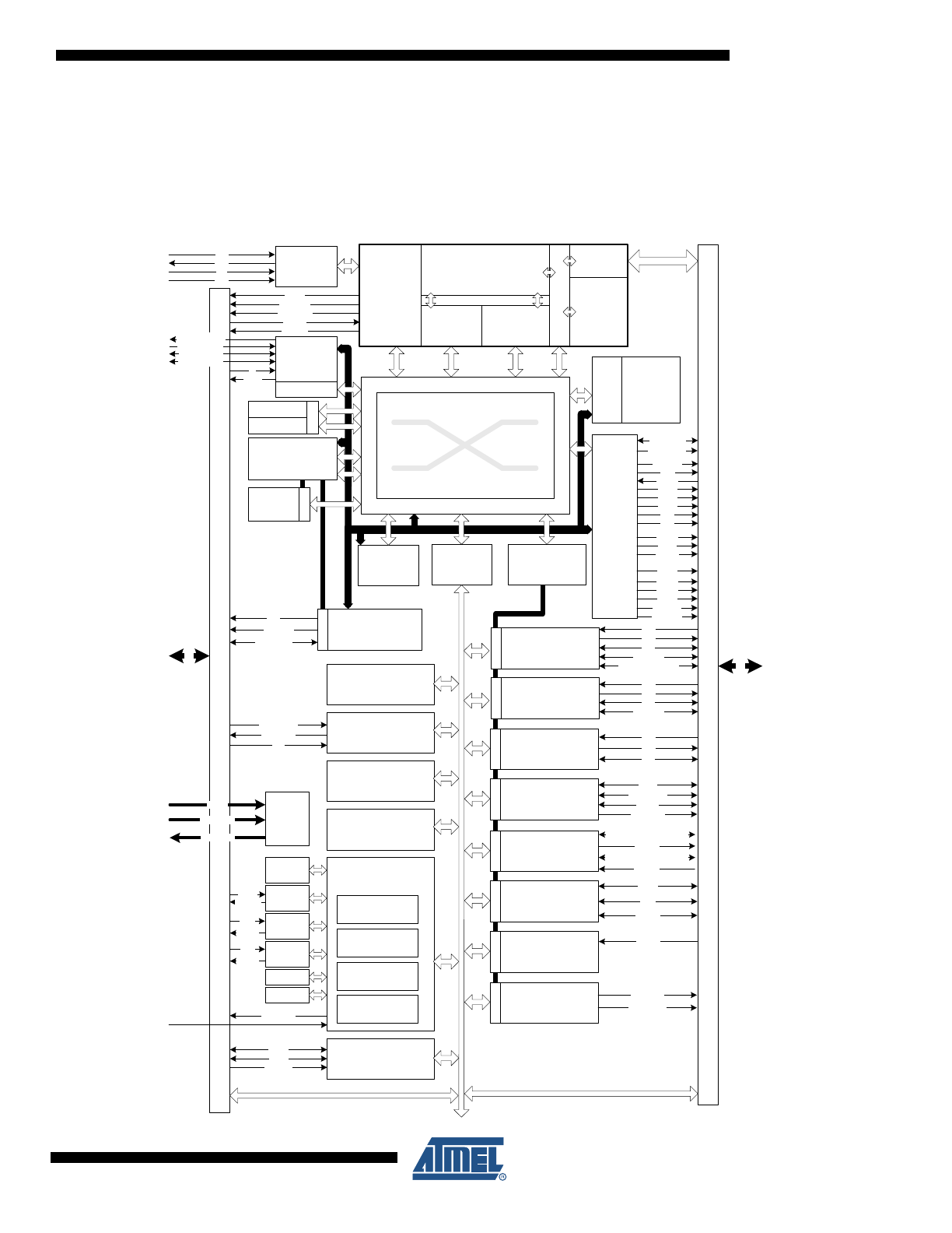
Overview
2.1
Block Diagram
Figure 2-1.
Block Diagram
AVR32UC
CPU
NEXUS
CLASS 2+
OCD
INSTR
INTERFACE
DATA
INTERFACE
TIMER/COUNTER
0/1
INTERRUPT
CONTROLLER
REAL TIME
COUNTER
PERIPHERAL
DMA
CONTROLLER
256/128/64
KB
FLASH
HSB-PB
BRIDGE B
HSB-PB
BRIDGE A
ME
MO
R
Y I
N
TE
R
FA
C
E
S
M
M
M
M
M
S
S
S
S
S
M
EXTERNAL
INTERRUPT
CONTROLLER
HIGH SPEED
BUS MATRIX
FAST GPIO
GE
N
E
RA
L P
U
RP
OS
E
IO
s
64 KB
SRAM
G
E
NE
RA
L P
URPOS
E
IO
s
PA
PB
PC
PX
A[2..0]
B[2..0]
CLK[2..0]
EXTINT[7..0]
SCAN[7..0]
NMI
GCLK[3..0]
XIN32
XOUT32
XIN0
XOUT0
PA
PB
PC
PX
RESET_N
E
X
TE
R
NAL
BUS I
N
TE
RF
ACE
(S
D
R
AM
, S
TA
TI
C
ME
MOR
Y
, C
O
MP
A
C
T
FL
ASH
& N
AND
FL
ASH
)
CAS
RAS
SDA10
SDCK
SDCKE
SDWE
NCS[5..0]
NRD
NWAIT
NWE0
DATA[15..0]
USB HS
INTERFACE
DMA
ID
VBOF
DMFS, DMHS
32 KHz
OSC
115 kHz
RCSYS
OSC0
PLL0
USART3
SERIAL
PERIPHERAL
INTERFACE 0/1
TWO-WIRE
INTERFACE 0/1
DM
A
DM
A
DM
A
RXD
TXD
CLK
MISO, MOSI
NPCS[3..1]
TWCK
TWD
USART1
DM
A
RXD
TXD
CLK
RTS, CTS
DSR, DTR, DCD, RI
USART0
USART2
DM
A
RXD
TXD
CLK
RTS, CTS
SYNCHRONOUS
SERIAL
CONTROLLER
DM
A
TX_CLOCK, TX_FRAME_SYNC
RX_DATA
TX_DATA
RX_CLOCK, RX_FRAME_SYNC
ANALOG TO
DIGITAL
CONVERTER
DM
A
AD[7..0]
WATCHDOG
TIMER
XIN1
XOUT1
OSC1
PLL1
SPCK
JTAG
INTERFACE
MCKO
MDO[5..0]
MSEO[1..0]
EVTI_N
EVTO_N
TCK
TDO
TDI
TMS
POWER
MANAGER
RESET
CONTROLLER
ADDR[23..0]
SLEEP
CONTROLLER
CLOCK
CONTROLLER
CLOCK
GENERATOR
FL
ASH
CO
N
TRO
LL
E
R
CONFIGURATION REGISTERS BUS
MEMORY PROTECTION UNIT
PB
PB
HSB
HSB
NWE1
NWE3
PB
A
PB
B
NPCS0
LOCAL BUS
INTERFACE
AUDIO
BITSTREAM
DAC
DM
A
DATA[1..0]
DATAN[1..0]
M
MULTIMEDIA CARD
& MEMORY STICK
INTERFACE
CLK
CMD[1..0]
DATA[15..0]
DM
A
S
AES
DM
A
CFCE1
CFCE2
CFRW
NANDOE
NANDWE
32KB RAM
32KB RAM
HR
A
M
0/
1
DPFS, DPHS
USB_VBIAS
USB_VBUS
S
S
VDDIN
VDDCORE
GNDCORE
DMACA
1V8
Regulator
TWALM
5
32072SH–AVR32–10/2012
AT32UC3A3
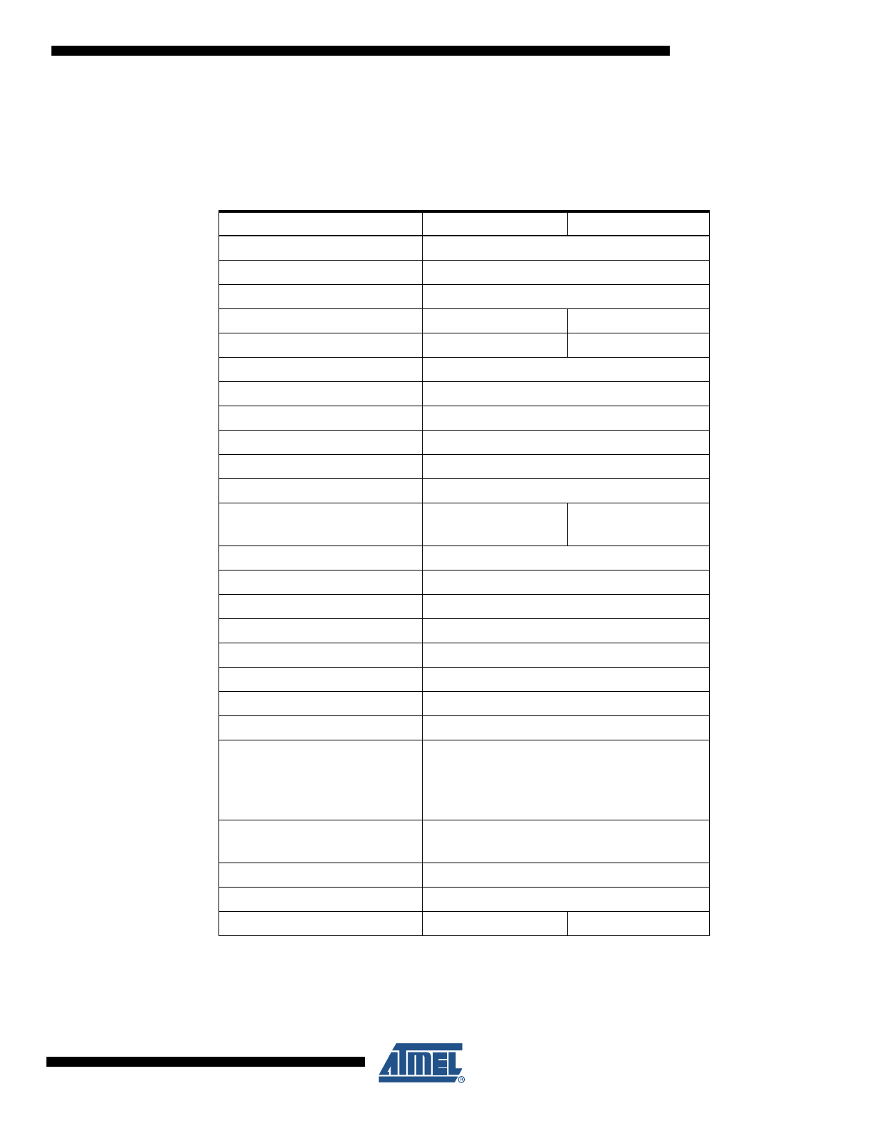
2.2
Configuration Summary
The table below lists all AT32UC3A3/A4 memory and package configurations:
Table 2-1.
Configuration Summary
Feature
AT32UC3A3256/128/64
AT32UC3A4256/128/64
Flash
256/128/64 KB
SRAM
64 KB
HSB RAM
64 KB
EBI
Full
Nand flash only
GPIO
110
70
External Interrupts
8
TWI
2
USART
4
Peripheral DMA Channels
8
Generic DMA Channels
4
SPI
2
MCI slots
2 MMC/SD slots
1 MMC/SD slot
+ 1 SD slot
High Speed USB
1
AES (S option)
1
SSC
1
Audio Bitstream DAC
1
Timer/Counter Channels
6
Watchdog Timer
1
Real-Time Clock Timer
1
Power Manager
1
Oscillators
PLL 80-240 MHz (PLL0/PLL1)
Crystal Oscillators 0.4-20 MHz (OSC0/OSC1)
Crystal Oscillator 32 KHz (OSC32K)
RC Oscillator 115 kHz (RCSYS)
10-bit ADC
number of channels
1
8
JTAG
1
Max Frequency
84 MHz
Package
LQFP144, TFBGA144
VFBGA100
6
32072SH–AVR32–10/2012
AT32UC3A3
3.
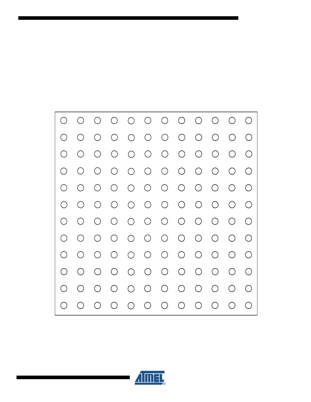
Package and Pinout
3.1
Package
The device pins are multiplexed with peripheral functions as described in the Peripheral Multi-
plexing on I/O Line section.
Figure 3-1.
TFBGA144 Pinout (top view)
12
11
10
9
8
7
6
5
4
3
2
1
A
B
C
D
E
F
G
H
J
K
L
M
PX40
PB00
PA28
PA27
PB03
PA29
PC02
PC04
PC05
DPHS
DMHS
USB_VBUS
PA09
GNDPLL
DMFS
USB_VBIAS
VDDIO
PC03
PB04
VDDIO
PB02
PA31
PB11
PX10
PX09
PX35
GNDIO
PX37
PX36
PB01
PX16
PX47
PX19
PB08
PA30
PX13
PA02
PB10
PX12
PA10
PA08
GNDCORE
DPFS
PB06
PB07
PA11
PA26
VDDIN
PA12
VDDCORE
PA07
PA25
PA06
PA16
PA13
PA05
PA04
PX53
VDDIO
PB09
PX15
PX49
PX48
GNDIO
GNDIO
PX08
VDDIO
PX54
PX38
PX07
PX06
PX39
PX50
PX51
GNDIO
GNDIO
PX05
PX59
PX00
PX57
VDDIO
PA17
PC01
VDDIO
PX58
PX01
PX56
PX55
PA15
PA14
PX02
PX34
PX04
PX46
PC00
PX52
PX17
PX44
GNDIO
PX03
PX20
VDDIO
PX43
PX18
GNDIO
PX45
PX11
PX14
PX21
PX24
PX23
PX41
PX42
PX22
PA23
PA01
PA00
PA03
PA24
VDDIO
PB05
VDDANA
PA22
PA21
PA19
RESET_N
TDO
TMS
PA20
PA18
TCK
PX29
GNDIO
PX27
VDDIN
TDI
GNDANA
PX28
PX26
PX25
PX33
PX30
PX31
PX32
7
32072SH–AVR32–10/2012
AT32UC3A3
Figure 3-2.
LQFP144 Pinout
U
SB_
V
BU
S
1
VD
D
IO
2
U
SB_
V
BIA
S
3
G
NDI
O
4
DM
HS
5
DP
HS
6
G
NDI
O
7
DM
FS
8
DP
FS
9
VD
D
IO
10
PB
08
11
PC
05
12
PC
04
13
PA
30
14
PA
02
15
PB
10
16
PB
09
17
PC
02
18
PC
03
19
G
NDI
O
20
VD
D
IO
21
PB
04
22
PA
29
23
PB
03
24
PB
02
25
PA
27
26
PB
01
27
PA
28
28
PA
31
29
PB
00
30
PB
11
31
PX
16
32
PX
13
33
PX
12
34
PX
19
35
PX
40
36
PX10
37
PX35
38
PX47
39
PX15
40
PX48
41
PX53
42
PX49
43
PX36
44
PX37
45
PX54
46
GNDIO
47
VDDIO
48
PX09
49
PX08
50
PX38
51
PX39
52
PX06
53
PX07
54
PX00
55
PX59
56
PX58
57
PX05
58
PX01
59
PX04
60
PX34
61
PX02
62
PX03
63
VDDIO
64
GNDIO
65
PX44
66
PX11
67
PX14
68
PX42
69
PX45
70
PX41
71
PX22
72
TD
I
10
8
TC
K
10
7
RES
ET
_N
10
6
TD
O
10
5
TM
S
10
4
VDDI
O
10
3
GN
D
IO
10
2
PA
15
10
1
PA
14
10
0
PC0
1
99
PC0
0
98
PX
31
97
PX
30
96
PX
33
95
PX
29
94
PX
32
93
PX
25
92
PX
28
91
PX
26
90
PX
27
89
PX
43
88
PX
52
87
PX
24
86
PX
23
85
PX
18
84
PX
17
83
GN
D
IO
82
VDDI
O
81
PX
21
80
PX
55
79
PX
56
78
PX
51
77
PX
57
76
PX
50
75
PX
46
74
PX
20
73
PA21
109
PA22
110
PA23
111
PA24
112
PA20
113
PA19
114
PA18
115
PA17
116
GNDANA
117
VDDANA
118
PA25
119
PA26
120
PB05
121
PA00
122
PA01
123
PA05
124
PA03
125
PA04
126
PA06
127
PA16
128
PA13
129
VDDIO
130
GNDIO
131
PA12
132
PA07
133
PB06
134
PB07
135
PA11
136
PA08
137
PA10
138
PA09
139
GNDCORE
140
VDDCORE
141
VDDIN
142
VDDIN
143
GNDPLL
144
8
32072SH–AVR32–10/2012
AT32UC3A3
Figure 3-3.
VFBGA100 Pinout (top view)
Note:
1. Those balls are physically connected to 2 GPIOs. Software must managed carrefully the GPIO
configuration to avoid electrical conflict
10
9
8
7
6
5
4
3
2
1
A
B
C
D
E
F
G
H
J
K
PA28
PA27
PB04
PA30
PC02
PC03
PC05
DPHS
DMHS
USB_VBUS
GNDPLL
DMFS
DPFS
PC04
VDDIO
VDDIO
PA29
PB02
PB01
PB00
PB11
PA31
GNDIO
PX10
PX13
PB03
PB09
PX16/
PX53
(1)
PB10
GNDIO
USB_VBIAS
PB08
PA09
PB06
PB07
PA10
PA11
VDDIN
VDDIN
PA06/
PA13
(1)
VDDCORE
PA04
PA08
GNDCORE
PA03
PX09
VDDIO
PA16
GNDIO
PX07
GNDIO
PA26/
PB05
(1)
VDDIO
PX12
GNDIO
PX08
PA02/
PX47
(1)
VDDIO
PX06
PX19/
PX59
(1)
PX00
PX30
PA12/
PA25
(1)
PA23/
PX46
(1)
PX01
PX02
PX05
PX25
PX31
TMS
PA22/
PX20
(1)
PX21
GNDIO
PX04
PX29
VDDIO
PA15/
PX45
(1)
VDDANA
PX24
PX26
PX03
PX15/
PX32
(1)
PC00/
PX14
(1)
PA14/
PX11
(1)
PC01
PX27
PX28
PX23
PA00/
PA18
(1)
PA01/
PA17
(1)
PA05
GNDANA
PA07/
PA19
(1)
PA20/
PX18
(1)
TDO
PA24/
PX17
(1)
RESET_N
TDI
PA21/
PX22
(1)
TCK

9
32072SH–AVR32–10/2012
AT32UC3A3
3.2
Peripheral Multiplexing on I/O lines
3.2.1
Multiplexed Signals
Each GPIO line can be assigned to one of the peripheral functions. The following table
describes the peripheral signals multiplexed to the GPIO lines.
Note that GPIO 44 is physically implemented in silicon but it must be kept unused and config-
ured in input mode.
Table 3-1.
GPIO Controller Function Multiplexing
BGA
144
QFP
144
BGA
100
PIN
G
P
I
O
Supply
PIN
Type
(2)
GPIO function
A
B
C
D
G11
122
G8
(1)
PA00
0
VDDIO
x3
USART0 - RTS
TC0 - CLK1
SPI1 - NPCS[3]
G12
123
G10
(1)
PA01
1
VDDIO
x1
USART0 - CTS
TC0 - A1
USART2 - RTS
D8
15
E1
(1)
PA02
2
VDDIO
x1
USART0 - CLK
TC0 - B1
SPI0 - NPCS[0]
G10
125
F9
PA03
3
VDDIO
x1
USART0 - RXD
EIC - EXTINT[4]
ABDAC - DATA[0]
F9
126
E9
PA04
4
VDDIO
x1
USART0 - TXD
EIC - EXTINT[5]
ABDAC - DATAN[0]
F10
124
G9
PA05
5
VDDIO
x1
USART1 - RXD
TC1 - CLK0
USB - ID
F8
127
E8
(1)
PA06
6
VDDIO
x1
USART1 - TXD
TC1 - CLK1
USB - VBOF
E10
133
H10
(1)
PA07
7
VDDIO
x1
SPI0 - NPCS[3]
ABDAC - DATAN[0]
USART1 - CLK
C11
137
F8
PA08
8
VDDIO
x3
SPI0 - SPCK
ABDAC - DATA[0]
TC1 - B1
B12
139
D8
PA09
9
VDDIO
x2
SPI0 - NPCS[0]
EIC - EXTINT[6]
TC1 - A1
C12
138
C10
PA10
10
VDDIO
x2
SPI0 - MOSI
USB - VBOF
TC1 - B0
D10
136
C9
PA11
11
VDDIO
x2
SPI0 - MISO
USB - ID
TC1 - A2
E12
132
G7
(1)
PA12
12
VDDIO
x1
USART1 - CTS
SPI0 - NPCS[2]
TC1 - A0
F11
129
E8
(1)
PA13
13
VDDIO
x1
USART1 - RTS
SPI0 - NPCS[1]
EIC - EXTINT[7]
J6
100
K7
(1)
PA14
14
VDDIO
x1
SPI0 - NPCS[1]
TWIMS0 - TWALM
TWIMS1 - TWCK
J7
101
J7
(1)
PA15
15
VDDIO
x1
MCI - CMD[1]
SPI1 - SPCK
TWIMS1 - TWD
F12
128
E7
PA16
16
VDDIO
x1
MCI - DATA[11]
SPI1 - MOSI
TC1 - CLK2
H7
116
G10
(1)
PA17
17
VDDANA
x1
MCI - DATA[10]
SPI1 - NPCS[1]
ADC - AD[7]
K8
115
G8
(1)
PA18
18
VDDANA
x1
MCI - DATA[9]
SPI1 - NPCS[2]
ADC - AD[6]
J8
114
H10
(1)
PA19
19
VDDANA
x1
MCI - DATA[8]
SPI1 - MISO
ADC - AD[5]
J9
113
H9
(1)
PA20
20
VDDANA
x1
EIC - NMI
SSC - RX_FRAME_SYNC
ADC - AD[4]
H9
109
K10
(1)
PA21
21
VDDANA
x1
ADC - AD[0]
EIC - EXTINT[0]
USB - ID
H10
110
H6
(1)
PA22
22
VDDANA
x1
ADC - AD[1]
EIC - EXTINT[1]
USB - VBOF
G8
111
G6
(1)
PA23
23
VDDANA
x1
ADC - AD[2]
EIC - EXTINT[2]
ABDAC - DATA[1]
G9
112
J10
(1)
PA24
24
VDDANA
x1
ADC - AD[3]
EIC - EXTINT[3]
ABDAC - DATAN[1]
E9
119
G7
(1)
PA25
25
VDDIO
x1
TWIMS0 - TWD
TWIMS1 - TWALM
USART1 - DCD
D9
120
F7
(1)
)
PA26
26
VDDIO
x1
TWIMS0 - TWCK
USART2 - CTS
USART1 - DSR
A4
26
A2
PA27
27
VDDIO
x2
MCI - CLK
SSC - RX_DATA
USART3 - RTS
MSI - SCLK
A3
28
A1
PA28
28
VDDIO
x1
MCI - CMD[0]
SSC - RX_CLOCK
USART3 - CTS
MSI - BS
A6
23
B4
PA29
29
VDDIO
x1
MCI - DATA[0]
USART3 - TXD
TC0 - CLK0
MSI - DATA[0]

10
32072SH–AVR32–10/2012
AT32UC3A3
C7
14
A4
PA30
30
VDDIO
x1
MCI - DATA[1]
USART3 - CLK
DMACA - DMAACK[0]
MSI - DATA[1]
B3
29
C2
PA31
31
VDDIO
x1
MCI - DATA[2]
USART2 - RXD
DMACA - DMARQ[0]
MSI - DATA[2]
A2
30
B1
PB00
32
VDDIO
x1
MCI - DATA[3]
USART2 - TXD
ADC - TRIGGER
MSI - DATA[3]
C4
27
B2
PB01
33
VDDIO
x1
MCI - DATA[4]
ABDAC - DATA[1]
EIC - SCAN[0]
MSI - INS
B4
25
B3
PB02
34
VDDIO
x1
MCI - DATA[5]
ABDAC - DATAN[1]
EIC - SCAN[1]
A5
24
C4
PB03
35
VDDIO
x1
MCI - DATA[6]
USART2 - CLK
EIC - SCAN[2]
B6
22
A3
PB04
36
VDDIO
x1
MCI - DATA[7]
USART3 - RXD
EIC - SCAN[3]
H12
121
F7
(1)
PB05
37
VDDIO
x3
USB - ID
TC0 - A0
EIC - SCAN[4]
D12
134
D7
PB06
38
VDDIO
x1
USB - VBOF
TC0 - B0
EIC - SCAN[5]
D11
135
D6
PB07
39
VDDIO
x3
SPI1 - SPCK
SSC - TX_CLOCK
EIC - SCAN[6]
C8
11
C6
PB08
40
VDDIO
x2
SPI1 - MISO
SSC - TX_DATA
EIC - SCAN[7]
E7
17
C5
PB09
41
VDDIO
x2
SPI1 - NPCS[0]
SSC - RX_DATA
EBI - NCS[4]
D7
16
D5
PB10
42
VDDIO
x2
SPI1 - MOSI
SSC - RX_FRAME_SYNC
EBI - NCS[5]
B2
31
C1
PB11
43
VDDIO
x1
USART1 - RXD
SSC - TX_FRAME_SYNC
PM - GCLK[1]
K5
98
K5
(1)
PC00
45
VDDIO
x1
H6
99
K6
PC01
46
VDDIO
x1
A7
18
A5
PC02
47
VDDIO
x1
B7
19
A6
PC03
48
VDDIO
x1
A8
13
B7
PC04
49
VDDIO
x1
A9
12
A7
PC05
50
VDDIO
x1
G1
55
G4
PX00
51
VDDIO
x2
EBI - DATA[10]
USART0 - RXD
USART1 - RI
H1
59
G2
PX01
52
VDDIO
x2
EBI - DATA[9]
USART0 - TXD
USART1 - DTR
J2
62
G3
PX02
53
VDDIO
x2
EBI - DATA[8]
USART0 - CTS
PM - GCLK[0]
K1
63
J1
PX03
54
VDDIO
x2
EBI - DATA[7]
USART0 - RTS
J1
60
H1
PX04
55
VDDIO
x2
EBI - DATA[6]
USART1 - RXD
G2
58
G1
PX05
56
VDDIO
x2
EBI - DATA[5]
USART1 - TXD
F3
53
F3
PX06
57
VDDIO
x2
EBI - DATA[4]
USART1 - CTS
F2
54
F4
PX07
58
VDDIO
x2
EBI - DATA[3]
USART1 - RTS
D1
50
E3
PX08
59
VDDIO
x2
EBI - DATA[2]
USART3 - RXD
C1
49
E4
PX09
60
VDDIO
x2
EBI - DATA[1]
USART3 - TXD
B1
37
D2
PX10
61
VDDIO
x2
EBI - DATA[0]
USART2 - RXD
L1
67
K7
(1)
PX11
62
VDDIO
x2
EBI - NWE1
USART2 - TXD
D6
34
D1
PX12
63
VDDIO
x2
EBI - NWE0
USART2 - CTS
MCI - CLK
C6
33
D3
PX13
64
VDDIO
x2
EBI - NRD
USART2 - RTS
MCI - CLK
M4
68
K5
(1)
PX14
65
VDDIO
x2
EBI - NCS[1]
TC0 - A0
E6
40
K4
(1)
PX15
66
VDDIO
x2
EBI - ADDR[19]
USART3 - RTS
TC0 - B0
C5
32
D4
(1)
PX16
67
VDDIO
x2
EBI - ADDR[18]
USART3 - CTS
TC0 - A1
K6
83
J10
(1)
PX17
68
VDDIO
x2
EBI - ADDR[17]
DMACA - DMARQ[1]
TC0 - B1
Table 3-1.
GPIO Controller Function Multiplexing
BGA
144
QFP
144
BGA
100
PIN
G
P
I
O
Supply
PIN
Type
(2)
GPIO function
A
B
C
D