
Features
•
High Performance, Low Power 32-bit AVR
®
Microcontroller
– Compact Single-Cycle RISC Instruction Set Including DSP Instructions
– Read-Modify-Write Instructions and Atomic Bit Manipulation
– Performance
• Up to 61 DMIPS Running at 48MHz from Flash (1 Flash Wait State)
• Up to 34 DMIPS Running at 24MHz from Flash (0 Flash Wait State)
•
Multi-Hierarchy Bus System
– High-Performance Data Transfers on Separate Buses for Increased Performance
– 7 Peripheral DMA Channels Improve Speed for Peripheral Communication
•
Internal High-Speed Flash
– 128Kbytes, and 64Kbytes Versions
– Single-Cycle Access up to 24MHz
– Prefetch Buffer Optimizing Instruction Execution at Maximum Speed
– 4ms Page Programming Time and 8ms Full-Chip Erase Time
– 100,000 Write Cycles, 15-year Data Retention Capability
– Flash Security Locks and User Defined Configuration Area
•
Internal High-Speed SRAM, Single-Cycle Access at Full Speed
– 16Kbytes
•
Interrupt Controller (INTC)
– Autovectored Low Latency Interrupt Service with Programmable Priority
•
External Interrupt Controller (EIC)
•
System Functions
– Power and Clock Manager
– SleepWalking
™
Power Saving Control
– Internal System RC Oscillator (RCSYS)
– 32 KHz Oscillator
– Clock Failure Detection
– One Multipurpose Oscillator and two Phase Locked Loop (PLL)
•
Windowed Watchdog Timer (WDT)
•
Asynchronous Timer (AST) with Real-Time Clock Capability
– Counter or Calendar Mode Supported
•
Frequency Meter (FREQM) for Accurate Measuring of Clock Frequency
•
Universal Serial Bus (USB)
– Device 2.0 full speed and low speed
– Flexible End-Point Configuration and Management
– On-chip Transceivers Including Pull-Ups
•
Three 16-bit Timer/Counter (TC) Channels
– External Clock Inputs, PWM, Capture and Various Counting Capabilities
•
7 PWM Channels (PWMA)
– 12-bit PWM up to 150MHz Source Clock
•
Three Universal Synchronous/Asynchronous Receiver/Transmitters (USART)
– Independent Baudrate Generator, Support for SPI
– Support for Hardware Handshaking
•
One Master/Slave Serial Peripheral Interfaces (SPI) with Chip Select Signals
– Up to 15 SPI Slaves can be Addressed
32133D–11/2011
32-bit AVR
®
Microcontroller
ATUC128D3
ATUC64D3
ATUC128D4
ATUC64D4
Summary

2
32133D–11/2011
UC3D
•
One Master and One Slave Two-Wire Interfaces (TWI), 400kbit/s I
2
C-compatible
•
One 8-channel Analog-To-Digital Converter (ADC)
•
One Inter-IC Sound Controller (IISC) with Stereo Capabilities
•
Autonomous Capacitive Touch Button (QTouch
®
) Capture
– Up to 25 Touch Buttons
– QWheel
®
and QSlide
®
Compatible
•
QTouch
®
Library Support
– Capacitive Touch Buttons, Sliders, and Wheels
– QTouch
®
and QMatrix
®
Acquisition
– Hardware assisted QTouch
®
Acquisition
•
One Programmable Glue Logic Controller(GLOC) for General Purpose PCB Design
•
On-Chip Non-Intrusive Debug System
– Nexus Class 2+, Runtime Control
– aWire
™
Single-Pin Programming and Debug Interface Muxed with Reset Pin
– 64-pin and 48-pin TQFP/QFN (51 and 35 GPIO Pins)
•
Four High-Drive I/O Pins
•
Single 3.3V Power Supply or Dual 1.8V-3.3V Power Supply

3
32133D–11/2011
UC3D
1. Description
The UC3D is a complete System-On-Chip microcontroller based on the AVR32UC RISC proces-
sor running at frequencies up to 48 MHz. AVR32UC is a high-performance 32-bit RISC
microprocessor core, designed for cost-sensitive embedded applications, with particular empha-
sis on low power consumption, high code density, and high performance.
The processor implements a fast and flexible interrupt controller for supporting modern operat-
ing systems and real-time operating systems.
Higher computation capability is achieved using a rich set of DSP instructions.
The Peripheral Direct Memory Access (DMA) controller enables data transfers between periph-
erals and memories without processor involvement. The Peripheral DMA controller drastically
reduces processing overhead when transferring continuous and large data streams.
The Power Manager improves design flexibility and security. Power monitoring is supported by
on-chip Power-On Reset (POR), and Brown-Out Detector (BOD). The device features several
oscillators, such as Oscillator 0 (OSC0), 32 KHz Oscillator and system RC oscillator (RCSYS),
and two Phase Lock Loop (PLL). Either of these oscillators/PLLs can be used as source for the
system clock.
The Watchdog Timer (WDT) will reset the device unless it is periodically serviced by the soft-
ware. This allows the device to recover from a condition that has caused the system to be
unstable.
The Asynchronous Timer (AST) combined with the 32KHz crystal oscillator supports powerful
real-time clock capabilities, with a maximum timeout of up to 136 years. The AST can operate in
counter mode or calendar mode. The 32KHz crystal oscillator can operate in a 1- or 2-pin mode,
trading pin usage and accuracy.
The Frequency Meter (FREQM) allows accurate measuring of a clock frequency by comparing it
to a known reference clock.
The Full-Speed USB 2.0 Device interface supports several USB Classes at the same time
thanks to the rich End-Point configuration.
The device includes three identical 16-bit Timer/Counter (TC) channels. Each channel can be
independently programmed to perform frequency measurement, event counting, interval mea-
surement, pulse generation, delay timing, and pulse width modulation.
The Pulse Width Modulation controller (PWMA) provides 12-bit PWM channels which can be
synchronized and controlled from a common timer. Seven PWM channels are available,
enabling applications that require multiple PWM outputs, such as LCD backlight control. The
PWM channels can operate independently, with duty cycles set independently from each other,
or in interlinked mode, with multiple channels changed at the same time.
The UC3D also features many communication interfaces for communication intensive applica-
tions. In addition to standard serial interfaces like USART, SPI or TWI, USB is available. The
USART supports different communication modes, like SPI mode.
A general purpose 8-channel ADC is provided; It features a fully configurable sequencer that
handles many conversions. Window Mode allows each ADC channel to be used like a simple
Analog Comparator.
The Inter-IC Sound controller (IISC) provides easy access to digital audio interfaces following
I2S stereo standard.

4
32133D–11/2011
UC3D
The Capacitive Touch (CAT) module senses touch on external capacitive touch sensors, using
the QTouch
®
technology. Capacitive touch sensors use no external mechanical components,
unlike normal push buttons, and therefore demand less maintenance in the user application.
The CAT module allows up to 25 touch sensors. One touch sensor can be configured to operate
autonomously without software interaction,allowing wakeup from sleep modes when activated.
Atmel also offers the QTouch library for embedding capacitive touch buttons, sliders, and
wheels functionality into AVR microcontrollers. The patented charge-transfer signal acquisition
offers robust sensing and included fully debounced reporting of touch keys and includes Adja-
cent Key Suppression
®
(AKS
®
) technology for unambiguous detection of key events. The easy-
to-use QTouch Suite toolchain allows you to explore, develop, and debug your own touch
applications.
The UC3D integrates a class 2+ Nexus 2.0 On-Chip Debug (OCD) System, with full-speed
read/write memory access, in addition to basic runtime control. The single-pin aWire interface
allows all features available through the JTAG interface to be accessed through the RESET pin,
allowing the JTAG pins to be used for GPIO or peripherals.
5
32133D–11/2011
UC3D
2. Overview
2.1
Block Diagram
Figure 2-1.
Block Diagram
SYSTEM CONTROL
INTERFACE
INTERRUPT
CONTROLLER
ASYNCHRONOUS
TIMER
PERIPHERAL
DMA
CONTROLLER
HSB-PB
BRIDGE B
HSB-PB
BRIDGE A
S
M
M
M
S
S
M
EXTERNAL INTERRUPT
CONTROLLER
HIGH SPEED
BUS MATRIX
G
E
NER
A
LP
U
R
P
O
SE
I/
Os
GE
NE
RA
L P
U
R
P
OS
E
I/
O
s
PA
PB
EXTINT[8..1]
NMI
GCLK[2..0]
PA
PB
SPI
DM
A
MISO, MOSI
NPCS[3..0]
USART0
USART1
USART2
DMA
RXD
TXD
CLK
RTS, CTS
WATCHDOG
TIMER
SCK
JTAG
INTERFACE
TDO
TDI
TMS
CONFIGURATION REGISTERS BUS
64/128KB
FLASH
S
FLASH
CO
NT
ROL
LER
UC CPU
NEXUS
CLASS 2+
OCD
INSTR
INTERFACE
DATA
INTERFACE
ME
MO
R
Y
IN
T
E
R
F
A
C
E
LOCAL BUS
16KB SRAM
LOCAL BUS
INTERFACE
FREQUENCY METER
PWM CONTROLLER
PWM[6..0]
TWI MASTER
DMA
TWI SLAVE
DM
A
8-CHANNEL ADC
INTERFACE
DM
A
AD[7..0]
ADVREF
POWER MANAGER
RESET
CONTROLLER
SLEEP
CONTROLLER
CLOCK
CONTROLLER
XIN32
XOUT32
OSC32K
RCSYS
XIN0
XOUT0
OSC0
PLL0
BOD
TCK
aWire
RESET_N
TWCK
TWD
TWCK
TWD
RC120M
PLL1
USB FS
CONTROLLER
M
INTER-IC SOUND
CONTROLLER
DM
A
DOUT
DIN
FSYNC
CLK
MCLK
DP
DM
VBUS
CAPACITIVE TOUCH
SENSOR
CONTROLLER
CSB[24..0]
CSA[24..0]
GLUE LOGIC
CONTROLLER
IN[15..0]
OUT[3:0]
TIMER/COUNTER
A[2..0]
B[2..0]
CLK[2..0]
DM
A
DATAOUT
6
32133D–11/2011
UC3D
2.2
Configuration Summary
Table 2-1.
Configuration Summary
Feature
ATUC128/64D3
ATUC128/64D4
Flash
128/64KB
128/64KB
SRAM
16KB
16KB
Package
TQFP64, QFN64
TQFP48, QFN48
GPIO
51
35
FS USB Device
1
Hi-drive pins
4
External Interrupts
9
7
TWI Master/Slave
1/1
USART
3
Peripheral DMA Channels
7
SPI
1
Asynchronous Timers
1
Timer/Counter Channels
3
PWM channels
7
Inter-IC Sound
1
Frequency Meter
1
Watchdog Timer
1
Power Manager
1
Oscillators
2x Phase Locked Loop 80-240 MHz (PLL)
1x Crystal Oscillator 0.4-20 MHz (OSC0)
1x Crystal Oscillator 32 KHz (OSC32K)
1x RC Oscillator 120MHz (RC120M)
1x RC Oscillator 115 kHz (RCSYS)
10-bit ADC channels
8
6
Capacitive Touch Sensor supported
25
17
Glue Logic Control Inputs/Outputs
16/4
14/4
JTAG
1
aWire
1
Max Frequency
48 MHz
7
32133D–11/2011
UC3D
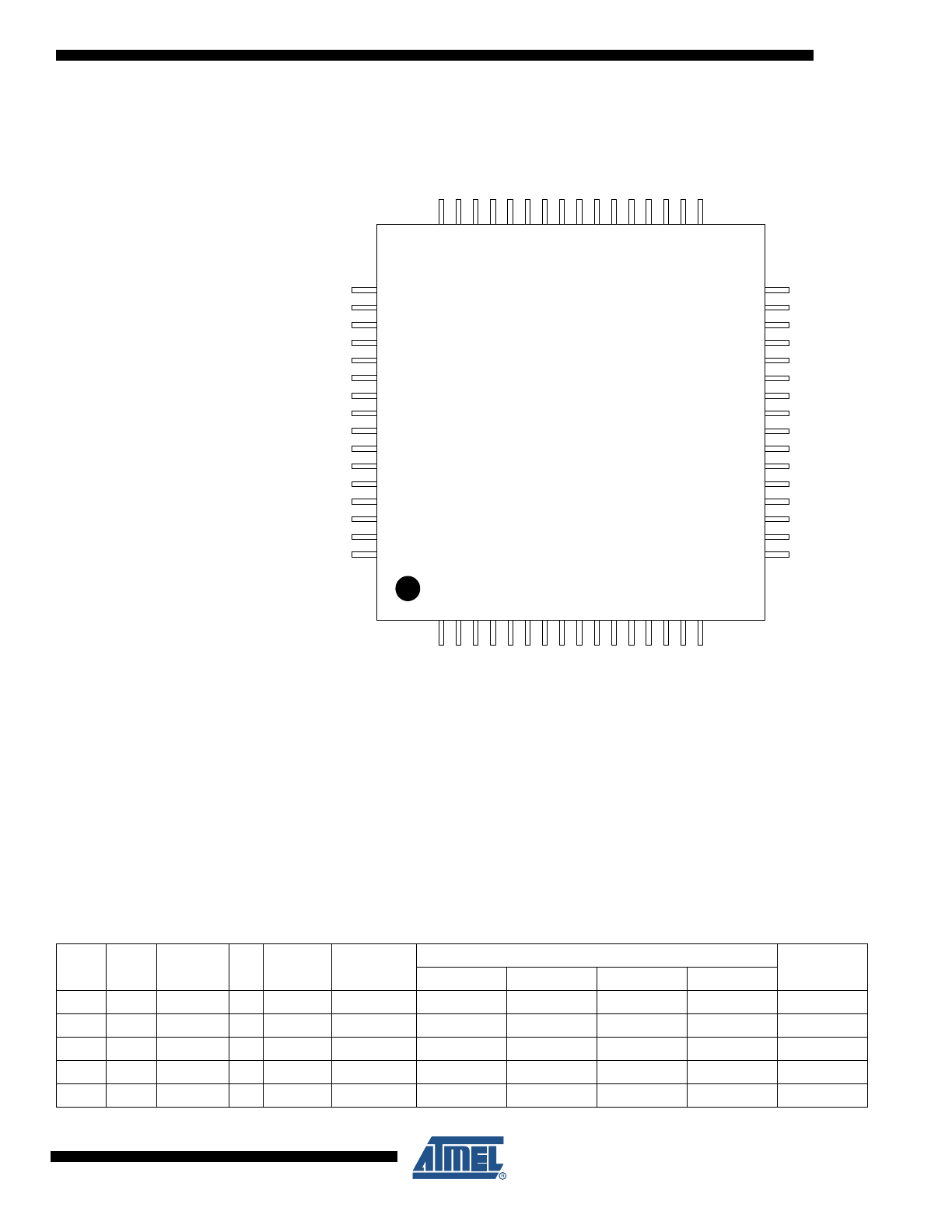
3. Package and Pinout
3.1
Package
The device pins are multiplexed with peripheral functions as described in
Section 3.2
.
Figure 3-1.
TQFP48/QFN48 Pinout
GND
1
PB
1
2
2
PA
0
0
3
PA
0
1
4
PA
0
2
5
PB
1
3
6
PA
0
3
7
PA
04
8
PA
0
5
9
PA
0
6
10
PA
0
7
11
PA
0
8
12
GNDANA
13
ADVREF
14
VDDANA
15
VDDOUT
16
VDDIN
17
VDDCORE
18
GND
19
PA09
20
PA10
21
PA11
22
PA12
23
VDDIO
24
VDD
IO
36
PA23
35
PA22
34
PA21
33
PA20
32
PA19
31
PA18
30
PA17
29
PA16
28
PA15
27
PA14
26
PA13
25
GND
37
PB14 - DP
38
PB15 - DM
39
PB16 - VBUS
40
PB17
41
PB18
42
PA24
43
PA25
44
PA26
45
PA27
46
RESET_N
47
VDDIO
48
8
32133D–11/2011
UC3D
Figure 3-2.
TQFP64/QFN64 Pinout
Note:
On QFN packages, the exposed pad is not connected to anything internally, but should be sol-
dered to ground to increase board level reliability.
3.2
Peripheral Multiplexing on I/O lines
3.2.1
Multiplexed signals
Each GPIO line can be assigned to one of the peripheral functions.The following table describes
the peripheral signals multiplexed to the GPIO lines.
GN
D
1
PB
12
2
PA
00
3
PA
01
4
PA
02
5
PB
00
6
PB
01
7
PB
13
8
PA
03
9
PA
04
10
PA
05
11
PA
06
12
PA
07
13
PA
08
14
PA
30
15
PA
31
16
GNDANA
17
ADVREF
18
VDDANA
19
VDDOUT
20
VDDIN
21
VDDCORE
22
GND
23
PB02
24
PB03
25
PB04
26
PB05
27
PA09
28
PA10
29
PA11
30
PA12
31
VDDIO
32
VDD
IO
48
PA23
47
PA22
46
PA21
45
PA20
44
PB07
43
PA29
42
PA28
41
PA19
40
PA18
39
PB06
38
PA17
37
PA16
36
PA15
35
PA14
34
PA13
33
GND
49
PB14 - DP
50
PB15 - DM
51
PB16-VBUS
52
PB17
53
PB08
54
PB09
55
PB18
56
PB10
57
PB11
58
PA24
59
PA25
60
PA26
61
PA27
62
RESET_N
63
VDDIO
64
Table 3-1.
Multiplexed Signals on I/O Pins
48-pin
Package
64-pin
Package
PIN
GPIO
Supply
Pad Type
GPIO Function
Other Functions
A
B
C
D
3
3
PA00
0
VDDIO
Normal I/O
SPI - MISO
PWMA - PWMA[1]
GLOC - IN[0]
CAT - CSB[0]
JTAG-TDI
4
4
PA01
1
VDDIO
Normal I/O
SPI - MOSI
PWMA - PWMA[2]
GLOC - IN[1]
CAT - CSA[1]
JTAG-TDO
5
5
PA02
2
VDDIO
Normal I/O
SPI - SCK
PWMA - PWMA[3]
GLOC - IN[2]
CAT - CSB[1]
JTAG-TMS
7
9
PA03
3
VDDANA
Analog I/O
PKGANA - ADCIN0
SCIF - GCLK[0]
GLOC - IN[5]
CAT - CSB[2]
8
10
PA04
4
VDDANA
Analog I/O
PKGANA - ADCIN1
SCIF - GCLK[1]
GLOC - IN[6]
CAT - CSA[3]

9
32133D–11/2011
UC3D
9
11
PA05
5
VDDANA
Analog I/O
EIC - EXTINT[8]
PKGANA - ADCIN2
GLOC - OUT[1]
CAT - CSB[3]
10
12
PA06
6
VDDANA
Analog I/O
EIC - EXTINT[1]
PKGANA - ADCIN3
GLOC - IN[7]
CAT - CSA[4]
11
13
PA07
7
VDDANA
Analog I/O
PWMA - PWMA[0]
PKGANA - ADCIN4
GLOC - IN[8]
CAT - CSB[4]
12
14
PA08
8
VDDANA
Analog I/O
PWMA - PWMA[1]
PKGANA - ADCIN5
GLOC - IN[9]
CAT - CSA[5]
20
28
PA09
9
VDDIO
Normal I/O, 5V
tolerant
TWIMS - TWCK
SPI - NPCS[2]
USART1 - CTS
CAT - CSB[5]
21
29
PA10
10
VDDIO
Normal I/O, 5V
tolerant
TWIMS - TWD
SPI - NPCS[3]
USART1 - RTS
CAT - CSA[6]
22
30
PA11
11
VDDIO
Normal I/O
USART0 - RTS
TC - A2
PWMA - PWMA[0]
CAT - CSB[6]
OSC32 - XIN
23
31
PA12
12
VDDIO
Normal I/O
USART0 - CTS
TC - B2
PWMA - PWMA[1]
CAT - CSA[7]
OSC32 - XOUT
25
33
PA13
13
VDDIO
Normal I/O
EIC - EXTINT[0]
PWMA - PWMA[2]
USART0 - CLK
CAT - CSB[7]
26
34
PA14
14
VDDIO
Normal I/O
SPI - MOSI
PWMA - PWMA[3]
EIC - EXTINT[2]
CAT - CSA[8]
27
35
PA15
15
VDDIO
Normal I/O
SPI - SCK
PWMA - PWMA[4]
USART2 - CLK
CAT - CSB[8]
28
36
PA16
16
VDDIO
Normal I/O
SPI - NPCS[0]
TC - CLK1
PWMA - PWMA[4]
CAT - CSA[9]
29
37
PA17
17
VDDIO
Normal I/O
SPI - NPCS[1]
TC - CLK2
SPI - SCK
CAT - CSB[9]
30
39
PA18
18
VDDIO
Normal I/O
USART0 - RXD
PWMA - PWMA[5]
SPI - MISO
CAT - CSA[10]
OSC0 - XIN
31
40
PA19
19
VDDIO
Normal I/O
USART0 - TXD
PWMA - PWMA[6]
SPI - MOSI
CAT - CSB[10]
OSC0 - XOUT
32
44
PA20
20
VDDIO
Normal I/O
USART1 - CLK
TC - CLK0
USART2 - RXD
CAT - CSA[11]
33
45
PA21
21
VDDIO
Normal I/O
PWMA - PWMA[2]
TC - A1
USART2 - TXD
CAT - CSB[11]
34
46
PA22
22
VDDIO
Normal I/O
PWMA - PWMA[6]
TC - B1
ADCIFD - EXTTRIG
CAT - CSA[12]
35
47
PA23
23
VDDIO
Normal I/O
USART1 - TXD
SPI - NPCS[1]
EIC - EXTINT[3]
CAT - CSB[12]
43
59
PA24
24
VDDIO
Normal I/O
USART1 - RXD
SPI - NPCS[0]
EIC - EXTINT[4]
CAT - CSB[15]
44
60
PA25
25
VDDIO
Normal I/O
SPI - MISO
PWMA - PWMA[3]
EIC - EXTINT[5]
CAT - CSA[16]
45
61
PA26
26
VDDIO
Normal I/O
IISC - IWS
USART2 - TXD
TC - A0
CAT - CSB[16]
46
62
PA27
27
VDDIO
Normal I/O
IISC - ISCK
USART2 - RXD
TC - B0
CAT - CSA[0]
41
PA28
28
VDDIO
Normal I/O
USART0 - CLK
PWMA - PWMA[4]
SPI - MISO
CAT - CSB[21]
42
PA29
29
VDDIO
Normal I/O
TC - CLK0
TC - CLK1
SPI - MOSI
CAT - CSA[22]
15
PA30
30
VDDANA
Analog I/O
PKGANA - ADCIN6
EIC - EXTINT[6]
SCIF - GCLK[2]
CAT - CSA[18]
16
PA31
31
VDDANA
Analog I/O
PKGANA - ADCIN7
EIC - EXTINT[7]
PWMA - PWMA[6]
CAT - CSB[18]
6
PB00
32
VDDIO
Normal I/O
TC - A0
EIC - EXTINT[4]
USART2 - CTS
CAT - CSA[17]
7
PB01
33
VDDIO
Normal I/O
TC - B0
EIC - EXTINT[5]
USART2 - RTS
CAT - CSB[17]
24
PB02
34
VDDIO
Normal I/O
EIC - EXTINT[6]
TC - A1
USART1 - TXD
CAT - CSA[19]
25
PB03
35
VDDIO
Normal I/O
EIC - EXTINT[7]
TC - B1
USART1 - RXD
CAT - CSB[19]
26
PB04
36
VDDIO
Normal I/O
USART1 - CTS
SPI - NPCS[3]
TC - CLK2
CAT - CSA[20]
27
PB05
37
VDDIO
Normal I/O
USART1 - RTS
SPI - NPCS[2]
PWMA - PWMA[5]
CAT - CSB[20]
38
PB06
38
VDDIO
Normal I/O
IISC - ISCK
PWMA - PWMA[5]
GLOC - IN[15]
CAT - CSA[21]
43
PB07
39
VDDIO
Normal I/O
IISC - ISDI
EIC - EXTINT[2]
GLOC - IN[11]
CAT - CSB[22]
54
PB08
40
VDDIO
Normal I/O
IISC - IWS
EIC - EXTINT[0]
GLOC - IN[14]
CAT - CSA[23]
55
PB09
41
VDDIO
Normal I/O
IISC - ISCK
IISC - IMCK
GLOC - IN[3]
CAT - CSB[23]
57
PB10
42
VDDIO
Normal I/O
IISC - ISDO
TC - A2
USART0 - RXD
CAT - CSA[24]
58
PB11
43
VDDIO
Normal I/O
IISC - IWS
TC - B2
USART0 - TXD
CAT - CSB[24]
Table 3-1.
Multiplexed Signals on I/O Pins
48-pin
Package
64-pin
Package
PIN
GPIO
Supply
Pad Type
GPIO Function
Other Functions
A
B
C
D
10
32133D–11/2011
UC3D
See
Section 4.
for a description of the various peripheral signals.
Refer to
”Electrical Characteristics” on page 37
for a description of the electrical properties of the
pad types used.
3.2.2
Peripheral Functions
Each GPIO line can be assigned to one of several peripheral functions. The following table
describes how the various peripheral functions are selected. The last listed function has priority
in case multiple functions are enabled.
3.2.3
JTAG Port Connections
If the JTAG is enabled, the JTAG will take control over a number of pins, irrespective of the I/O
Controller configuration.
2
2
PB12
44
VDDIO
Normal I/O
SPI - NPCS[0]
IISC - IMCK
GLOC - OUT[0]
JTAG-TCK
6
8
PB13
45
VDDIO
Normal I/O
CAT - SYNC
SCIF - GCLK[2]
GLOC - IN[4]
CAT - CSA[2]
38
50
PB14
46
VDDIO
Normal I/O
USBC - DP
USART0 - RXD
GLOC - OUT[2]
CAT - CSA[13]
39
51
PB15
47
VDDIO
Normal I/O
USBC - DM
USART0 - TXD
GLOC - IN[12]
CAT - CSB[13]
40
52
PB16
48
VDDIO
Input only, 5V
tolerant
USBC - VBUS
GLOC - IN[10]
USB-VBUS
41
53
PB17
49
VDDIO
Normal I/O
IISC - ISDO
USART0 - RTS
GLOC - IN[13]
42
56
PB18
50
VDDIO
Normal I/O
IISC - ISDI
CAT - SYNC
GLOC - OUT[3]
CAT - CSA[15]
Table 3-1.
Multiplexed Signals on I/O Pins
48-pin
Package
64-pin
Package
PIN
GPIO
Supply
Pad Type
GPIO Function
Other Functions
A
B
C
D
Table 3-2.
Peripheral Functions
Function
Description
A
GPIO peripheral selection A
B
GPIO peripheral selection B
C
GPIO peripheral selection C
D
GPIO peripheral selection D
Table 3-3.
JTAG Pinout
48-pin or 64-pin
Package
Pin Name
JTAG Pin
2
PB12
TCK
5
PA02
TMS
4
PA01
TDO
3
PA00
TDI